
Infinera unveils its next-gen packet-optical platforms
 Source: Infinera
Infinera has unveiled its latest metro products that support up to 200-gigabit wavelengths using CFP2-DCO pluggable modules.
The XTM II platform family is designed to support growing metro traffic, low-latency services and the trend to move sophisticated equipment towards the network edge. Placing computing, storage and even switching near the network edge contrasts with the classical approach of backhauling traffic, sometimes deep within the network.
“If you backhaul everything, you really do not know if it belongs in that part of the network,” says Geoff Bennett, director, solutions and technology at Infinera. Backhauling inherently magnifies traffic whereas operators want greater efficiencies in dealing with bandwidth growth, he says: “This is where the more cloud-like architectures towards the network edge come in.”
But locating equipment at the network edge means it must fit within existing premises or in installed prefabricated huts where space and the power supplied are constrained.
“If you are asking service providers to put more complex equipment there, then you need low power utilisation,” says Bennett. “This has been a key piece of feedback from customers we have been asking as to how they want our existing products to evolve in the metro-access.”
Having a distributed switch fabric is a long-term advantage for Infinera
Infinera says its latest XTM II products are eight times denser in terms of tranmission capacity while setting a new power-consumption low of 20W-27W per 100 gigabits depending on the operating temperature (25oC to 55oC). Infinera claims its nearest metro equipment competitor achieves 47W per 100 gigabits.
Sterling Perrin, principal analyst, optical networking and transport at Heavy Reading, says Infinera has achieved the power-efficient design by using a distributed switch architecture rather that a central switch fabric and adopting the CFP2-DCO pluggable module with its low-power coherent DSP.
“If you have a centralised fabric and you put it into an edge application then for some cases it will be a perfect fit but for many applications, it will be overkill in terms of capacity and hence power,” says Perrin. “Infinera is able to do it in a modular fashion in terms of just how much capacity and power is put in an application.”
Having a distributed switch fabric is a long-term advantage for Infinera for these applications, says Perrin, whereas competitor vendors will also benefit from the CFP2-DCO for their next designs.
And even if a competitor uses a distributed design, they will not leapfrog Infinera, says Perrin, although he expects competitors’ designs to come down considerably in power with the adoption of the CFP2-DCO.
Infinera has chosen not to use its photonic integrated circuit (PIC) technology for its latest metro platform given the large installed base of XTM chassis that already use pluggable modules. “It would make sense that customers would give feedback that they want a product that has industry-leading performance but which is also backwards compatible,” says Bennett.
Infinera has said it will evaluate whether its PIC technology will be applied to each new generation of the product line. “So when you get to the XTM III they will have another round looking at it,” says Perrin. “If I were placing bets on the XTM III, I would say they are going to continue down this route [of using pluggables].”
Perrin expects line-side pluggable technology to continue to progress with companies such as Acacia Communications and the collaboration between Ciena with its WaveLogic DSP technology and several optical module makers.
“At what point is the PIC going to be better than what is available with the pluggables?” says Perrin. “For this application, I don’t see it.”
XTM II family
Infinera has already been shipping upgraded XTM chassis for the last 18 months in advance of the launch of its latest metro cards. The upgraded chassis - the one rack unit (1RU) TM-102/II, the 3RU TM-301/II and the 11RU TM-3000/II - all feature enhanced power management and cooling.
What Infinera is unveiling now are three cards that enhance the capacity and features of the enhanced chassis. The new cards will work with the older generation XTM chassis (without the ‘II’ suffix) as long as a vacant card slot is available and the chassis’ total power supply is not exceeded. This is important given over 30,000 XTM chassis have been deployed.
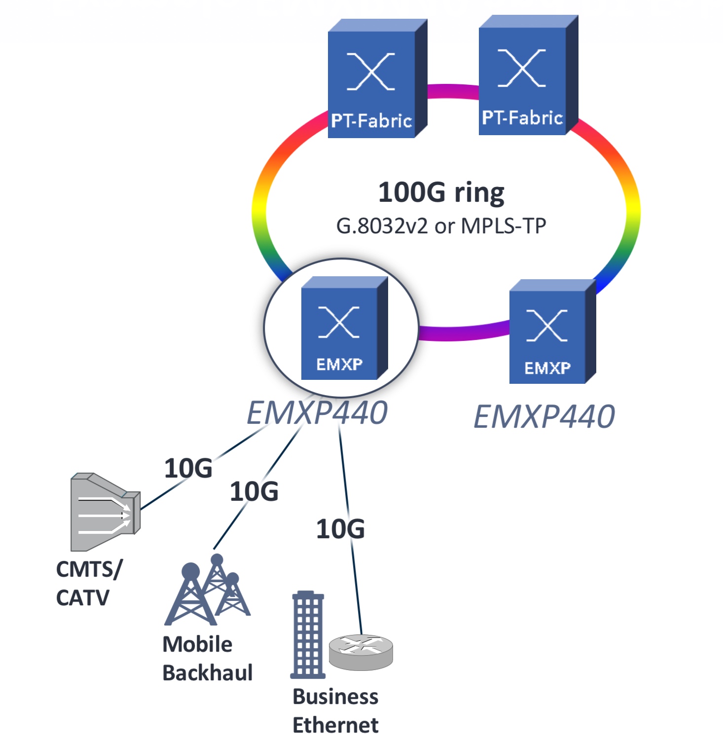
The Infinera cards announced are the 400-flexponder, a 200-gigabit muxponder, and the EMXP440 packet-optical transport switch. The distributed switch architecture is implemented using the EMXP440 card.
Operators will also be offered Infinera’s Instant Bandwidth feature as part of the XTM II whereby they can pay for the line side capacity they use: either 100-gigabit or 200-gigabit wavelengths using the CFP2-DCO. The Instant Bandwidth offered is not the superchannel format available for Infinera’s other platforms that use its PIC but it does offer operators the option of deploying a higher-speed wavelength when needed and paying later.
400G flexponder
The flexponder can operate as a transponder and as a muxponder. For a transponder, the client signal and line-side data rate operate at the same data rate. In contrast, a muxponder aggregates lower data-rate client signals for transport on a single wavelength.
Infinera’s 400-gigabit flexponder card uses four 100 Gigabit Ethernet QSFP28 client interfaces and two 200-gigabit CFP2-DCO pluggable line-side modules. Each CFP2-DCO can transport data at 100 gigabits using polarisation-multiplexing, quadrature phase-shift keying (PM-QPSK) modulation or at 200 gigabits using 16-ary quadrature amplitude modulation (PM-16QAM).
The 400-gigabit card can thus operate as a transponder when the CFP2-DCO transports at 100 gigabits and as a muxponder when it carries two 100-gigabit signals over a 200-gigabit lambda. Given the card has two CFP2 line-side modules, it can even operate as a transponder and muxponder simultaneously.
The flexponder card also supports OTN block encryption using the AES-256 symmetric key protocol.
The flexponder is an upgrade on Infinera’s existing 100-gigabit muxponder card. The eightfold increase in capacity is achieved by using two 200-gigabit ports instead of a single 100-gigabit module and halving the width of the line card.
Using the flexponder card, the TM-102/II chassis has a transport capacity of 400 gigabits, up to 1.6 terabits with the TM-301/II and a total of 4 terabits using the TM-3000/II platform.
We can dial back the FEC if you need low latency and don't need the reach
200G muxponder
The double-width 200G card includes all the electronics needed for multi-service multiplexing. The line-side optics is a single CFP2-DCO module whereas the client side can accommodate two QSFP28s and 12 SFP+ 10-gigabit modules. The card can multiplex a mix of services including 10GbE, 40GbE, and 100GbE; 8-, 16- and 32-gigabit Fibre Channel; OTN and legacy SONET/SDH traffic.
Other features include support for OTN block encryption using the AES-256 symmetric key protocol.
The card’s forward error correction performance can also be traded to reduce the traffic latency. “We can dial back the FEC if you need low latency and don't need the reach,” says Bennett.
OTN add-drop multiplexing can also be implemented by pairing two of the multiplexer cards.
EMXP440 switch and flexible open line system
The EMXP440 packet-optical transport switch card supports layer-two functionality such as Carrier Ethernet 2.0 and MPLS-TP. “Mobile backhaul and residential broadband, these are the cards the operators tend to use,” says Bennett.
The two-slot EMXP440 card has two CFP2-DCOs and 12 SFP+ client-side interfaces. The reason why the line side and client side interface capacity differ (400 gigabits versus 120 gigabits) is that the card can be used to build simple packet rings (see diagram, top).
The line-side interfaces can be used for ‘East’ and ‘West' traffic while the SFP+ modules can be used to add and drop signals. The EMXP440 card also has an MPO port such that up to 12 SFP+ further ports can be added using Infinera’s PTIO-10G card, part of its PT Fabric products.
A flexible grid open line system is also available for the XTM II. The XTM II’s 100-gigabit and 200-gigabit wavelengths fit within a 50GHz-wide fixed grid channel but Infinera is already anticipating future higher baud rates that will require channels wider than 50GHz. A flexible grid also improves the use of the fibre’s overall capacity. In turn, RAMAN amplification will also be needed to extend the reach using future higher order modulation schemes such as 32- and 64-QAM.
Infinera says the 400-gigabit flexponder card will be available in the next quarter while the 200-gigabit muxponder and the EMXP440 cards will ship in the final quarter of 2017.
Creating a long-term view for the semiconductor industry
The semiconductor industry is set for considerable change over the next 15 years.
“We are at an inflection point in the history of the [chip] industry,” says Thomas Conte, an IEEE Fellow. “It will be very different and very diverse; there won’t be one semiconductor industry.”
Conte (pictured) is co-chair of the IEEE Rebooting Computing initiative that is sponsoring the International Roadmap of Devices and Systems (IRDS) programme (See The emergence of the IRDS, below). The IRDS is defining technology roadmaps over a 15-year horizon and in November will publish its first that spans nine focus areas.
The focus of the IRDS on systems and devices and the broadening of technologies being considered is a consequence of the changing dynamics of the chip industry.
Conte stresses that it is not so much the ending of Moore’s Law that is causing the change as the ending of CMOS. Transistors will still continue to shrink even though it is becoming harder and costlier to achieve but the scaling benefits that for decades delivered a constant power density for chips with each new CMOS process node ended a decade ago.
“Back in the day it was pretty easy to plot it [the roadmap] because the technology was rather static in what we wanted to achieve,” says Conte. That ‘cushy ride’ that CMOS has delivered is ending. “The question now is: Are there other technologies we should be investing in that help applications move forward?” says Conte.
Focus groups
The IRDS has set up nine focus groups and in March published the first white papers from the teams.
The most complete white paper is from the More Moore focus group which looks at how new generations of smaller transistor features will be achieved. “It is clear that for the next 10 to 15 years we still have a lot of CMOS nodes left,” says Conte. “We still have to track what happens to CMOS.”
Conte says it is becoming clearer that ICs, in general, are going to follow the course of flash memory and be constructed as 3D monolithic designs. “We are just beginning to understand how to do this," says Conte.
"This does not mean we are going to get transistors that make computing faster without doing something different,” he says. This explains the work of the Beyond CMOS (Emerging Research Devices) focus team that is looking at alternative non-CMOS technologies to advance systems performance.
It is clear that for the next 10 to 15 years we still have a lot of CMOS nodes left
A third IRDS focus group is Outside System Connectivity which includes interface technologies such as photonic interconnect needed for future systems. “Outside System Interconnect is an important focus group and it is also our interface to the IEEE 5G roadmap team,” he says.
Conte also highlights two other IRDS focus teams: System and Architecture, and Applications Benchmarking. “These two focus teams are really important as to what the IRDS is all about,” says Conte.
The System and Architecture group has identified four systems views that it will focus on: the data centre, mobile handsets and tablets, edge devices for the Internet of Things, and control systems for the cyber-physical world such as automation, robotics and automotive systems.
The Application Benchmarking focus group is tasked with predicting key applications, quantifying how their performance is evolving and identifying roadblocks that could hinder their progress. Feature recognition, an important machine learning task, is one such example.
The IRDS is also continuing the working format established by the ITRS whereby every odd year a new 15-year roadmap is published while updates are published every even year.
Roadmapping
Three communities contribute to the development of the IRDS roadmap: industry, government and academia.
Industry is more concerned with solving their immediate problems and do not have the time or resources to investigate something that might or might not work in 15 years’ time, says Conte. Academia, in contrast, is more interested in addressing challenging problems over a longer term, 15-year horizon. Government national labs in the US and Europe’s imec sit somewhere in between and try to come up with mid-range solutions. “It is an interesting tension and it seems to work,” says Conte.
Contributors to the IRDS are from the US, Europe, Japan, South Korea and Taiwan but not China which is putting huge effort to be self-sufficient in semiconductors.
“We have not got participation for China yet,” says Conte. “It is not that we are against that, we just have not made the connections yet.” Conte believes China’s input would be very good for the roadmap effort. “They are being very aggressive and bright and they are more willing to take risks than the West,” he says.
What will be deemed a success for the IRDS work?
“It is to come up with a good prediction that is 15 years out and identify what the roadblocks are to getting there.”
____________________________________________________________
The emergence of the IRDS
The IRDS was established in 2016 by the IEEE after it took over the roadmap work of the International Technology Roadmap for Semiconductors (ITRS), an organisation sponsored by the five leading chip manufacturing regions in the world.
“The [work of the] ITRS was a bottoms-up roadmap, driven by the semiconductor industry,” says Conte. “It started with devices and didn't really go much higher.”
With the end of scaling, whereby the power density of chips remained constant with each new CMOS process node, the ITRS realised its long-established roadmap work needed a rethink which resulted in the establishment of ITRS 2.0.
“The ITRS 2.0 was an attempt to do a top-down approach looking at the system level and working down to devices,” says Conte. It was well received by everyone but the sponsors, says Conte, which was not surprising given their bottoms-up focus. It resulted in the sponsors of the ITRS 2.0 such as the US Semiconductor Industry Association (SIA) pulling out and the IEEE stepping in.
“This is much closer to what we are trying to do with the Rebooting Computing so it makes sense this group comes into the IEEE band and we act as a sponsor,” says Conte.
Packaging silicon photonics using passive alignment
- An Israeli start-up is tackling a key packaging challenge for silicon photonics
Teramount has developed a way to simplify the packaging of silicon photonics chips. Instead of using active alignment whereby an external laser is required to carefully align a fibre to the optical die, the Israeli start-up has developed a technology that allows passive alignment.
 Hesham Taha“If we want silicon photonics to ramp up to volume, it has to meet CMOS standards both in terms of fabrication and packaging,” says Hesham Taha, Teramount's CEO.
Taha worked at a company developing atomic force microscopy systems before co-founding Teramount. "We got to know of the problem of injecting light into a waveguide and were surprised that the industry was still using active alignment," he says.
This spurred Taha and a colleague to develop optical solutions to match a single-mode fibre core to an optical waveguide, and they founded Teramount in Jerusalem in 2013. "We started real activity at the beginning of 2015 after getting funding," says Taha.
Existing silicon photonics companies either develop their own customised active alignment equipment or outsource the activity to a third party. "If we solve one of the bottlenecks of silicon photonics in terms of packaging, silicon photonics will be more and more adopted," says Taha.
If we want silicon photonics to ramp up to volume, it has to meet CMOS standards both in terms of fabrication and packaging
The design
Teramount's solution includes two elements: a PhotonicsPlug that is flip-chipped onto the silicon photonics die while still part of a wafer, and a 'bump', a design element added on the silicon photonics chip next to the optical waveguide. "Our solution, which we will be selling, is the PhotonicsPlug and we do require them [the designers] to add one element [the bump] to their silicon photonics chip," says Taha.
The main PhotonicsPlug component is a silicon die comprising optics that manipulates the beam using self-aligning optics and focusses it onto the silicon photonics chip via a glass spacer. Teramount’s die also has V-grooves to interface the single-mode ribbon fibre. Teramount says its die is made using an inexpensive mature CMOS process due to the relatively large feature sizes of the optical elements.
The second design element - the bump - is added next to the silicon photonics chip's grating coupler. The grating coupler is one of two techniques used in the industry to interface a fibre to the waveguide, the other being edge coupling.
“We want to place it [the bump] next to the waveguide so that the optics of the PhotonicPlug works in conjunction with it so that it brings the beam to the waveguide with a large tolerance,” says Taha. The bump is accurately placed on the chip using standard lithography techniques.
The resulting tolerance with which the die can be attached to the silicon photonics wafer is up to ± 20 microns in each of the three dimensions such that standard flip-chip machines can attach the PhotonicsPlug to the wafer.
“Flip-chip machines today work with a tolerance of ± 6 microns and can do 1,500 assemblies per hour,” says Taha.
"This is the main philosophy we are bringing here," he says. "Instead of the accurate placement of the fibre next to the grating coupler which requires active alignment, we want to replace that with a cheaper alignment technique that has much better accuracy at the wafer level," says Taha.
Status
Teramount has already shown working devices using the technology. In addition, Teramount is working with several partners and has demonstrated its technology with their silicon photonics chip designs. "With these partners we are doing the integration and qualifying the performance of the device," says Taha. "We will finalise at least two of these partnerships within a few months."
The start-up is also working to enable volume manufacturing by bringing its technology to industrial fabrication plants. This will be completed in the next few months.
Being a small start-up, the company is focussed on developing the grating coupler solution but it has already started work on an edge-coupling technique to a device’s waveguides. Edge coupling is suited to wavelength-division multiplexing (WDM) silicon photonics chips. That is because grating couplers are wavelength-dependent while edge coupling supports a broader range of wavelengths.
What the cable operators are planning for NFV and SDN
Cable operators are working on adding wireless to their fixed access networks using NFV and SDN technologies.
 Don Clarke“Cable operators are now every bit as informed about NFV and SDN as the telcos are, but they are not out there talking too much about it,” says Don Clarke, principal architect for network technologies at CableLabs, the R&D organisation serving the cable operators.
Clarke is well placed to comment. While at BT, he initiated the industry collaboration on NFV and edited the original white paper which introduced the NFV concept and outlined the operators’ vision for NFV.
NFV plans
The cable operators are planning developments by exploiting the Central Office Re-architected as a Datacenter (CORD) initiative being pursued by the wider telecom community. Comcast is one cable operator that has already joined the Open Networking Lab’s (ON.Lab) CORD initiative. The aim is to add a data centre capability to the cable operators’ access network onto which wireless will be added.
CableLabs is investigating adding high-bandwidth wireless to the cable network using small cells, and the role 5G will play. The cable operators use DOCSIS as their broadband access network technology and it is ideally suited for small cells once these become mainstream, says Clarke: “How you overlay wireless on top of that network is probably where there is going to be some significant opportunities in the next few years.”
One project CableLabs is working on is helping cable operators provision services more efficiently. At present, operators deliver services over several networks: DOCSIS, EPON and in some cases, wireless. CableLabs has been working for a couple of years on simplifying the provisioning process so that the system is agnostic to the underlying networks. “The easiest way to do that is to abstract and virtualize the lower-level functionality; we call that virtual provisioning,” says Clarke.
CableLabs recently published its Virtual Provisioning Interfaces Technical Report on this topic and is developing data models and information models for the various access technologies so that they can be abstracted. The result will be more efficient provisioning of services irrespective of the underlying access technology, says Clarke.
How you overlay wireless on top of that network is probably where there is going to be some significant opportunities in the next few years
SNAPS
CableLabs is also looking at how to virtualise functionality cable operators may deploy near the edge of their networks.
“As the cable network evolves to do different things and adds more capabilities, CableLabs is looking at the technology platform that would do that,” says Clarke.
To this aim, CableLabs has created the SDN-NFV Application development Platform and Stack - SNAPS - which it has contributed to the Open Platform for NFV (OPNFV) group, part of the open source management organisation, The Linux Foundation.
SNAPS is a reference platform to be located near the network edge, and possibly at the cable head-end where cable operators deliver video over their networks. The reference platform makes use of the cloud-based operating system, OpenStack, and other open source components such as OpenDaylight, and is being used to instantiate virtual network functions (VNFs) in a real-time dynamic way. “The classic NFV vision,” says Clarke.
CableLabs' Randy Levensalor says one challenge facing cable operators is that, like telcos, they have separate cloud infrastructures for their services and that impacts their bottom line.
Cable operators are now every bit as informed about NFV and SDN as the telcos are, but they are not out there talking too much about it
“You have one [cloud infrastructure] for business services, one for video delivery and one for IT, and you are operationally less efficient when you have those different stacks,” says Levensalor, lead software architect at CableLabs. “With SNAPS, you bring together all the capabilities that are needed in a reference configuration that can be replicated.”
This platform can support local compute with low latency. "We are not able to say much but there is a longer-term vision for that capability that we’ll develop new applications around,” says Clarke.
Challenges and opportunities
The challenges facing cable operators concerning NFV and SDN are the same as those facing the telcos, such as how to orchestrate and manage virtual networks and do it in a way that avoids vendor lock-in.
“The whole industry wants an open ecosystem where we can buy virtual network functions from one vendor and connect them to virtual network functions and other components from different vendors to create an end-to-end platform with the best capabilities at any given time,” says Clarke.
He also believes that cable operators can move more quickly than telcos because of how they collaborate via CableLabs, their research hub. However, the cable operators' progress is inevitably linked to that of the telcos given they want to use the same SDN and NFV technologies to achieve economies of scale. “So we can’t diverge in the areas that need to be common, but we can move more quickly in areas where the cable network has an inherent advantage, for example in the access network,” says Clarke.
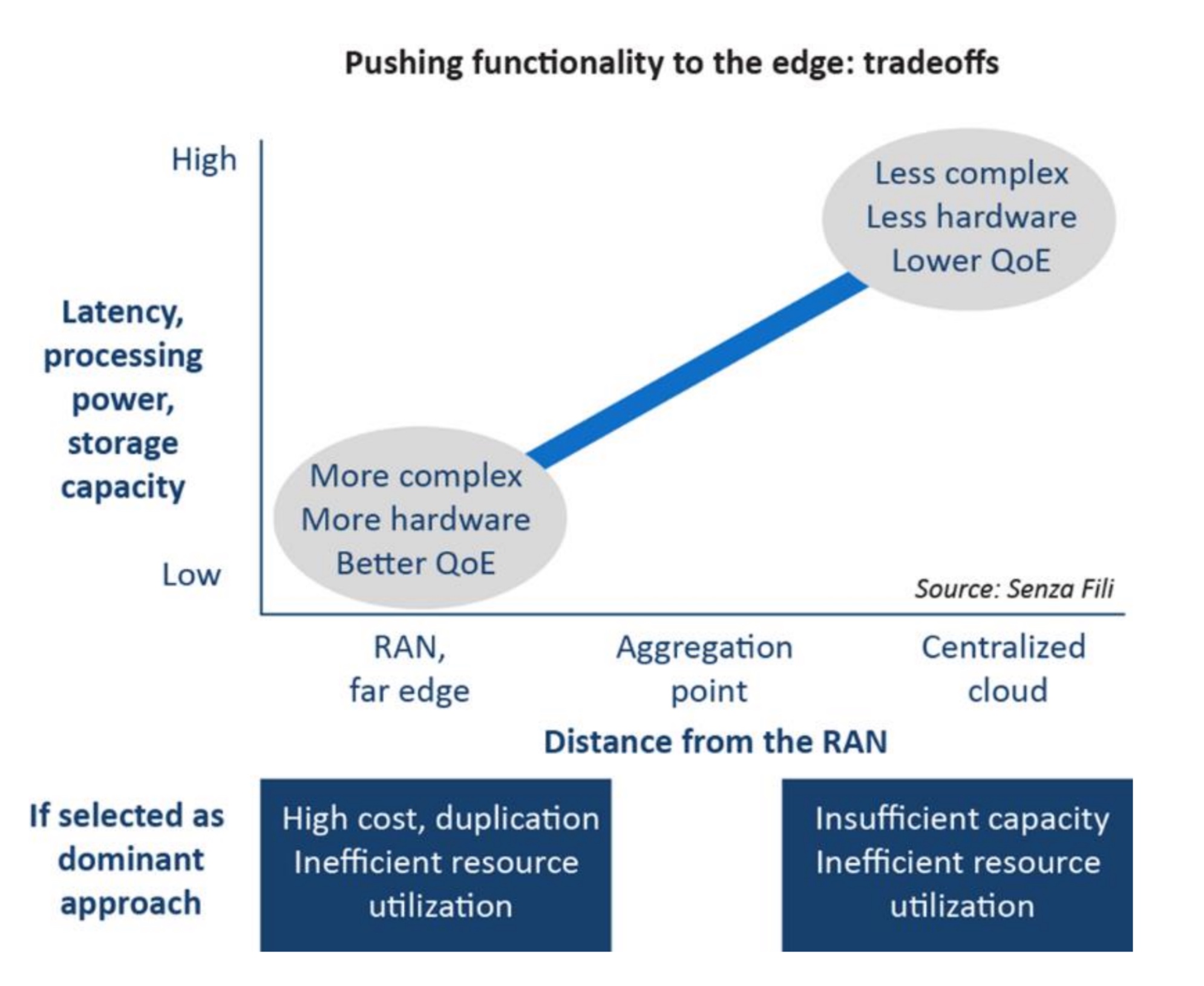
Giving telecom networks a computing edge
But a subtler approach is taking hold as networks evolve whereby what a user does will change depending on their location. And what will enable this is edge computing.
 Source: Senza Fili Consulting
Edge computing
“This is an entirely new concept,” says Monica Paolini, president and founder at Senza Fili Consulting. “It is a way to think about service which is going to have a profound impact.”
Edge computing has emerged as a consequence of operators virtualising their networks. Virtualisation of network functions hosted in the cloud has promoted a trend to move telecom functionality to the network core. Functionality does not need to be centralised but initially, that has been the trend, says Paolini, especially given how virtualisation promotes the idea that network location no longer matters.
“That is a good story, it delivers a lot of cost savings,” says Paolini, who recently published a report on edge computing. *
But a realisation has emerged across the industry that location does matter; centralisation may save the operator some costs but it can impact performance. Depending on the application, it makes sense to move servers and storage closer to the network edge.
The result has been several industry initiatives. One is Mobile Edge Computing (MEC) being developed by the European Telecommunications Standards Institute (ETSI). In March, ETSI renamed the Industry Specification Group undertaking the work to Multi-access Edge Computing to reflect the operators requirements beyond just cellular.
“What Multi-access Edge Computing does is move some of the core functionality from a central location to the edge,” says Paolini.
Another initiative is M-CORD, the mobile component of the Central Office Re-architected as a Datacenter initiative, overseen by the Open Networks Labs non-profit organisation. Other initiatives Paolini highlights include the Open Compute Project, Open Edge Computing and the Telecom Infra Project.
This is an entirely new concept. It is a way to think about service which is going to have a profound impact.
Location
The exact location of the ‘edge’ where the servers and storage reside is not straightforward.
In general, edge computing is located somewhere between the radio access network (RAN) and the network core. Putting everything at the RAN is one extreme but that would lead to huge duplication of hardware and exceed what RAN locations can support. Equally, edge computing has arisen in response to the limitations of putting too much functionality in the core.
The matter of location is blurred further when one considers that the RAN itself is movable to the core using the Cloud RAN architecture.
Paolini cites another reason why the location of edge computing is not well defined: the industry does not yet know. And it will only be in the next year or two when operators start trialling the technology. “There is going to be some trial and error by the operators,” she says.
Use cases
An enterprise located across a campus is one example use of edge computing, given how much of the content generated stays on-campus. If the bulk of voice calls and data stay local, sending traffic to the core and back makes little sense. There are also security benefits keeping data local. An enterprise may also use the edge computing to run services locally and share them across networks, for example using cellular or Wi-Fi for calls.
Another example is to install edge computing at a sports stadium, not only to store video of the game’s play locally - again avoiding going to the core and back with content - but also to cache video from games taking place elsewhere for viewing by attending fans.
Virtual reality and augmented reality are other applications that require low-latency, another performance benefit of having local computation.
Paolini expects the uptake of edge computing to be gradual. She also points to its challenging business case, or at least how operators typically assess a business case may not tell the full story.
Operators view investing in edge computing as an extra cost but Paolini argues that operators need to look carefully at the financial benefits. Edge computing delivers better utilisation of the network and lower latency. “The initial cost for multi-access edge computing is compensated for by the improved utilisation of the existing network,” she says.
When Paolini started the report it was to research low-latency and the issues of distributed network design, reliability and redundancy. But she soon realised that multi-access edge computing was something broader and that edge computing is beyond what ETSI is doing.
This is not like an operator rolling out LTE and reporting to shareholders how much of the population now has coverage. “It is a very different business to learn how to use networks better,” says Paolini.
* Click here to access the report, Power at the edge. MEC, edge computing, and the prominence of location
ETSI embraces AI to address rising network complexity
The growing complexity of networks is forcing telecom operators and systems vendors to turn to machine intelligence for help. It has led the European Telecommunications Standards Institute, ETSI, to set up an industry specification group to define how artificial intelligence (AI) can be applied to networking.
“With the advent of network functions virtualisation and software-defined networking, we can see the eventuality that network management is going to get very much more complicated,” says Ray Forbes, convenor of the ETSI Industry Specification Group, Experimental Network Intelligence (ISG-ENI).
 Source: ETSI
The AI will not just help with network management, he says, but also with the introduction of services and the more efficient use of network resources.
Visibility of events at many locations in the network will be needed with the deployment of network functions virtualisation (NFV), says Forbes. In current networks, a large switch may serve hundreds of thousands of users but with NFV, virtual network functions will be at many locations. The ETSI group will look at how AI can be used to manage and control this distributed deployment of virtual network functions, says Forbes.
The group’s work has started by inviting interested parties to bring and discuss use cases from which a set of requirements will be generated. In parallel, the group is looking at AI techniques.
The aim is to use computing to derive data from across the network. The data will be analysed, and by having 'context awareness', the machine intelligence will compute various scenarios before presenting the most promising ones for consideration by the network management team. “The process is collecting data, analysing it, testing out various scenarios and then advising people on what would happen in the better scenarios,” says Forbes.
With the advent of NFV and SDN, we can see the eventuality that network management is going to get very much more complicated
ETSI's goal is to make it easier for operators to deploy services quickly, reroute around networking faults, and make better use of networking resources. “In very large cities like Shanghai and Tokyo, where there are populations of 25 million, there is a need for this,” says Forbes. “In London, with about 12 million people, there is still a need but not quite so quickly.”
Operators and system vendors have some understanding of AI but there is a learning curve in bringing more and more AI experts on board, says Forbes: "Hence, we are trying to involve various universities in the research project."
Project schedule
The ISG-ENI's initial document work will be followed by defining the architecture and specifying the parameters needed to measure the network and the 'intelligence' of the scenarios.
“ETSI has a two-year project with the possibility of an extension,” says Forbes, with AI deployed in networks as early as 2019.
Forbes says open-source software to add AI to networks could be available as soon as 2018. Such open-source software will be developed by operators and systems vendors rather than ETSI.
BT bolsters research in quantum technologies
BT is increasing its investment in quantum technologies. “We have a whole team of people doing quantum and it is growing really fast,” says Andrew Lord, head of optical communications at BT.
The UK incumbent is working with companies such as Huawei, ADVA Optical Networking and ID Quantique on quantum cryptography, used for secure point-to-point communications. And in February, BT joined the Telecom Infra Project (TIP), and will work with Facebook and other TIP members at BT Labs in Adastral Park and at London’s Tech City. Quantum computing is one early project.
 Andrew LordThe topics of quantum computing and data security are linked. The advent of quantum computers promises the break the encryption schemes securing data today, while developments in quantum cryptography coupled with advances in mathematics promise new schemes resilient to the quantum computer threat.
Securing data transmission
To create a secure link between locations, special digital keys are used to scramble data. Two common data encryption schemes are used, based on symmetric and asymmetric keys.
A common asymmetric key scheme is public key cryptography which uses a public and private key pair that are uniquely related. The public key is published along with its user’s name. Any party wanting to send data securely to the user looks up their public key and uses it to scramble the data. Only the user, which has the associated private key, can unscramble the data. A widely used public-key crypto-system is the RSA algorithm.
There are algorithms that can be run on quantum computers that can crack RSA. Public key crypto has a big question mark over it in the future and anything using public key crypto now also has a question mark over it.
In contrast, symmetric schemes use the same key at both link ends, to lock and unlock the data. A well-known symmetric key algorithm is the Advanced Encryption Standard which uses keys up to 256-bits long (AES-256); the more bits, the more secure the encryption.
The issue with a symmetrical key scheme, however, is getting the key to the recipient without it being compromised. One way is to deliver the secret key using a security guard handcuffed to a case. An approach more befitting the digital age is to send the secret key over a secure link, and here, public key cryptography can be used. In effect, an asymmetric key is used to encrypt the symmetric key for transmission to the destination prior to secure communication.
But what worries governments, enterprises and the financial community is the advent of quantum computing and the risk it poses to cracking public key algorithms which are the predominant way data is secured. Quantum computers are not yet available but government agencies and companies such as Intel, Microsoft and Google are investing in their development and are making progress.
Michele Mosca estimates that there is a 50 percent chance that a quantum computer will exist by 2030. Professor Mosca, co-founder of the Institute for Quantum Computing at the University of Waterloo, Canada and of the security firm, evolutionQ, has a background in cyber security and has researched quantum computing for 20 years.
This is a big deal, says BT’s Lord. “There are algorithms that can be run on quantum computers that can crack RSA,” he says. “Public key crypto has a big question mark over it in the future and anything using public key crypto now also has a question mark over it.”
A one-in-two chance by 2030 suggests companies have time to prepare but that is not the case. Companies need to keep data confidential for a number of years. This means that they need to protect data to the threat of quantum computers at least as many years in advance since cyber-criminals could intercept and cache the data and wait for the advent of quantum computers to crack the coded data.
Upping the game
The need to have secure systems in place years in advance of quantum computer systems is leading security experts and researchers to pursue two approaches to data security. One uses maths while the other is based on quantum physics.
Maths promises new algorithms that are not vulnerable to quantum computing. These are known as post-quantum or quantum-resistant techniques. Several approaches are being researched including lattice-based, coding-based and hash-function-based techniques. But these will take several years to develop. Moreover, such algorithms are deemed secure because they are based on sound maths that is resilient to algorithms run on quantum computers. But equally, they are secure because techniques to break them have not been widely investigated, by researchers and cyber criminals alike.
The second, physics approach uses quantum mechanics for key distribution across an optical link, which is inherently secure.
“Do you pin your hopes on a physics theory [quantum mechanics] that has been around for 100 years or do you base it on maths?” says BT’s Lord. “Or do you do both?”
In the world of the very small, things are linked, even though they are not next to each other
Quantum cryptography
One way to create a secure link is to send the information encoded on photons - particles of light. Here, each photon carries a single bit of the key.
If the adversary steals the photon, it is not received and, equally, they are taking information that is no use to them, says Lord. A more sophisticated technique is to measure the photon while it passes through but here they come up against the quantum mechanical effect where measuring a photon changes its parameters. The transmitter and receiver typically reserve at random a small number of the key’s photons to detect a potential eavesdropper. If the receiver detects photons that were not sent, the change alerts them that the link has been compromised.
The issue with such quantum key distribution techniques is that the distances a single photon can be sent are limited to a few tens of kilometres only. If longer links are needed, intermediate secure trusted sites are used to regenerate the key. These trusted sites need to be secure.
Entanglement, whereby two photons are created such that they are linked even if they are physically in separate locations, is one way researchers are looking to extend the distance keys can be distributed. With such entangled photons, any change or measurement of one instantly affects the twin photon. “In the world of the very small, things are linked, even though they are not next to each other,” says Lord.
Entanglement could be used by quantum repeaters to increase the length possible for key distribution not least for satellites, says Lord: “A lot of work is going on how to put quantum key distribution on orbiting satellites using entanglement.”
But quantum key distribution only solves a particular class of problem such as protecting data sent across links, backing up data between a bank and a data centre, for example. The technique is also dependent on light and thus is not as widely applicable as post-quantum algorithms. "There is a view emerging in the industry that you throw both of these techniques [post quantum algorithms and quantum key distribution] especially at data streams you want to keep secure."
Practicalities
BT working with Toshiba and optical transport equipment maker ADVA Optical Networking have already demonstrated a quantum protected link operating at 100 gigabits-per-second.
BT’s Lord says that while quantum cryptography has been a relatively dormant topic for the last decade, this is now changing. “There are lots of investment around the world and in the UK, with millions poured in by the government,” he says. BT is also encouraged that there are more companies entering the market including Huawei.
“What is missing is still a little bit more industrialisation,” says Lord. “Quantum physics is pretty sound but we still need to check that the way this is implemented, there are no ways of breaching it; to be honest we haven't really done that yet.”
BT says it has spent the last few months talking to financial institutions and claims there is much interest, especially with quantum computing getting much closer to commercialisation. “That is going to force people to make some decisions in the coming years,” says Lord.
Infinera inches closer to cognitive networking
The second and final part as to how optical networking is becoming smarter
Infinera says it has made it easier for operators to deploy optical links to accommodate traffic growth.
The system vendor says its latest capability, known as Instant Network, also paves the way for autonomous networks that will predict traffic trends and enable capacity as required.
 The latest announcement builds on Infinera’s existing Instant Bandwidth feature, introduced in 2012, that uses its photonic integrated circuit (PIC) technology.
Instant Bandwidth exploits the fact that all five 100-gigabit wavelengths of a line card hosting Infinera’s 500-gigabit PIC are lit even though an operator may only need a subset of the 100-gigabit wavelengths. Using Instant Bandwidth, extra capacity can be added to a link - until all five wavelengths are used - in a matter of hours.
The technology allows 100-gigabit wavelengths to be activated in minutes, says Geoff Bennett, director, solutions and technology at Infinera (pictured). It takes several hours due to the processing time for the operator to raise a purchasing order for the new capacity and get it signed off.
Instant Bandwidth has been enhanced since its introduction. Infinera has introduced its latest generation 2.4 terabit PIC which is also sliceable. With a sliceable PIC, individual wavelengths can be sent to different locations using reconfigurable optical add-drop multiplexer (ROADM) technology within the network.
Another feature added is time-based Instant Bandwidth. This allows an operator to add extra capacity without first raising a purchase order. Paying for the extra capacity is dealt with at a later date. This feature has already benefited operators that have experienced a fibre cut and have used Instant Bandwidth to reroute traffic.
Infinera says over 70 of its customers use Instant Bandwidth. These include half of its long-haul customers, its top three submarine network customers and over 60 percent of its data centre interconnect players that use its Cloud Xpress and XTS products. Some of its data centre interconnect customers request boxes with all the licences already activated, says Bennett.
The internet content providers are banging the drum for cognitive networking
Instant Network
Now, with the Instant Network announcement, Infinera has added a licence pool and moveable licences. The result is that an operator can add capacity in minutes rather than hours by using its pool of prepaid licenses.
Equally, if an operator wants to reroute a 100-gigabit or 200-gigabit wavelength to another destination, it can transfer the same licence from the original end-point to the new one.
“They [operators] can activate capacity when the revenue-generating service asks for it,” says Bennett.
Another element of Instant Network still to be introduced is the Automated Capacity Engineering that is part of Infinera’s Xceed software.
 Source: Infinera
“Automated Capacity Engineering will be an application that runs on Xceed,” says Bennett. The Automated Capacity Engineering is an application running on the OpenDaylight open source software-defined networking (SDN) controller that takes advantage of plug-ins that Infinera has added to the Xceed platform such as multi-layer path computation and traffic monitoring.
Using this feature, the SDN orchestrator can request a 100 Gigabit Ethernet private line, for example. If there is insufficient capacity, the Automated Capacity Engineering app will calculate the most cost-effective path and install the necessary licences at the required locations, says Bennett.
“We think this is leading the way to cognitive networking,” he says. “We have the software foundation and the hardware foundation for this.”
Networks that think
With a cognitive network, data from the network is monitored and fed to a machine learning algorithm to predict when capacity will be exhausted. New capacity can then be added in a timely accordingly.
Bennett says internet content providers, the likes of Google, Microsoft and Facebook, will all deploy such technology in their networks.
Being consumers of huge amounts of bandwidth, they will be the first adopters. Wholesale operators which also serve the internet content providers will likely follow. Traditional telecom operators with their more limited traffic growth will be the last to adopt such technology.
But cognitive networking is not yet ready. “The machine learning algorithms are still basic,” says Bennett. “But the biggest thing that is missing is the acceptance [of such technology] by network operations staff.”
However, this is not an issue with the internet content providers. “They are banging the drum for cognitive networking,” says Bennett.
Part 1: Ciena's Liquid Spectrum, click here
Real-time visibility makes optical networking smarter
Systems vendors are making optical networks smarter. Their latest equipment, combining intelligent silicon and software, can measure the status of the network and enable dynamic network management.
Ciena recently announced its Liquid Spectrum networking product while Infinera has launched its Instant Network. Both vendors exploit the capabilities of their latest generation coherent DSPs to allow greater network automation and efficiency. The vendors even talk about their products being an important step towards autonomous or cognitive networks.
"Operators need to do things more efficiently," says Helen Xenos, director, portfolio solutions marketing at Ciena. "There is a lot of unpredictability in how traffic needs to be connected over the network." Moreover, demands on the network are set to increase with 5G and the billions of devices to be connected with the advent of Internet of Things.
Existing optical networks are designed to meet worse-case conditions. Margins are built into links based on the fibre used and assumptions are made about the equipment's end-of-life performance and the traffic to be carried. Now, with Ciena's latest WaveLogic Ai coherent DSP-ASIC, not only is the performance of the network measured but the coherent DSP can be used to exploit the network's state rather than use the worse-case end-of-life conditions. "With Liquid Spectrum, you now don't need to operate the network in a static mode," says Xenos.
We are at the beginning of this new world of operating networks
Software applications
Ciena has announced the first four software applications as part of Liquid Spectrum. The first, Performance Meter, uses measured signal-to-noise ratio data from the coherent DSP-ASICs to gauge the network's state to determine how efficiently the network is operating.
Bandwidth Optimiser acts on the network planner's request for bandwidth. The app recommends the optimum capacity that can be run on the link, based on exploiting baud rate and the reach, and also where to place the wavelengths within the C-band spectrum. Moreover, if service demands change, the network engineer can decide to reduce the built-in margins. "I may decide I don't need to reserve a 3dB margin right now and drop it down to 1dB," says Xenos. Bandwidth Optimiser can then be rerun to see how the new service demand can be met.
This approach contrasts with the existing way end points are connected, where all the wavelengths used are at the same capacity, a user decides their wavelengths and no changes are made once the wavelengths are deployed. "It is much simpler, it [the app] takes away complexity from the user," says Xenos.
 The Liquid Restoration app ensuring alternative capacity in response to the loss of a 300-gigabit route due to a fault. Source: Ciena
The two remaining apps launched are Liquid Restoration and Wave-Line Synchroniser. Liquid Restoration looks at all the available options if a particular path fails. "It will borrow against margin to get as much capacity as possible," says Xenos. Wave-Line Synchroniser is a tool that helps with settings so that Ciena's optics can work with another vendor's line system or optics from another vendor work with Ciena's line system.
Liquid Spectrum will be offered as a bundle as part of Ciena's latest BluePlanet Manage, Control and Plan tool that combines service and network management, resource control and planning.
Xenos says Liquid Spectrum represents the latest, significant remaining piece towards the industry's goal of developing an agile optical infrastructure. Sophisticated reconfigurable optical add-drop multiplexers (ROADMs) and flexible coherent DSPs have existed for a while but how such flexible technology has been employed has been limited because of the lack of knowledge of the real-time state of the network. Moreover, with these latest Liquid Spectrum software tools, much of the manual link engineering and complexity regarding what capacity can be supported and where in the spectrum it should be placed, says Xenos.
"We are at the beginning of this new world of operating networks," says Xenos. "Going forward, there will be an increasingly level of sophistication that will be built into the software."
Ciena demonstrated Liquid Spectrum at the OFC show held in Los Angeles last month.
Part 2: Infinera's Instant Network, click here
An insider's view on the merits of optical integration

Tolstikhin is president and CEO of Intengent, the Ottawa-based consultancy and custom design service provider, and an industry veteran of photonic integration. In 2005 he founded OneChip Photonics, a fabless maker of indium phosphide photonic integrated circuits for optical access.
One important lesson he learned at OneChip was how the cost benefit of a photonic integrated circuit (PIC) can be eroded with a cheap optical sub-assembly made from discrete off-the-shelf components. When OneChip started, the selling price for GPON optics was around $100 a unit but this quickly came down to $6. "We needed sales in volumes and they never came close to meeting $6," says Tolstikhin.
OneChip changed strategy, seeing early the emerging opportunity for 100-gigabit optics for the data centre but despite being among the first to demonstrate fully integrated 100-gigabit transmitter and receiver chips – at OFC 2013 – the company eventually folded.
When OneChip started, the selling price for GPON optics was around $100 a unit but this quickly came down to $6
Integent can be seen as the photonic equivalent of an electronic ASIC design house that was common in the chip industry, acting as the intermediary between an equipment vendor commissioning a chip design and the foundry making the chip.
Integent creates designs for system integrators which it takes to a commercial foundry for manufacturing. The company makes stand-alone devices, device arrays, and multi-function PICs. Integent uses the regrowth-free taper-assistant vertical integration (TAVI) indium phosphide process of the California-based foundry Global Communication Semiconductors (GCS). "We have also partnered with a prominent PIC design house, VLC Photonics, for PIC layout and verification testing,” says Tolstikhin. Together, Intengent, VLC and GCS offer a one-stop-shop for the development and production of PICs.
III-V and silicon photonics
Tolstikhin is a big fan of indium phosphide and related III-V semiconductor materials, pointing out that they can implement all the optical functions required for telecom and datacom applications. He is a firm believer that III-V will continue to be the material system of choice for various applications and argues that silicon photonics is not so much a competitor to III-V but a complement.
"Silicon photonics needs indium-phosphide-based sources but also benefits from III-V modulators and detectors, which have better performance than their silicon photonics counterparts," he says.
He admits that indium phosphide photonics cannot compete with the PIC scalability that silicon photonics offers. But that will benefit indium phosphide as silicon photonics matures. Intengent already benefits from this co-existence, offering specialised indium phosphide photonic chip development for silicon photonics as well.
"Silicon photonics cannot compete with indium phosphide photonics in relatively simple yet highest volume optical components for telecom and datacom transceivers," says Tolstikhin. Partly this is due to silicon photonics' performance inferiority but mainly for economical reasons.
Silicon photonics will have its chance, but only where it beats competing technologies on fundamentals, not just cost
There are also few applications that need monolithic photonic integration. Tolstikhin highlights coherent optics as one example but that is a market with limited volumes. Meanwhile, the most promising emerging market - transceivers for the data centre, whether 100-gigabit (4x25G NRZ) PSM or CWDM4 designs or in future 400-gigabit (4x100G PAM4) transceivers, will likely be implemented using optical sub-assembly and hybrid integration technologies.
Tolstikhin may be a proponent of indium phosphide but he does not dismiss silicon photonics' prospects: "It will have its chance, but only where it beats competing technologies on fundamentals, not just cost."
One such area is large-scale optoelectronic systems, such as data processors or switch fabrics for large-scale data centres. These are designs that cannot be assembled using discretes and go beyond the scalability of indium phosphide PICs. "This is not silicon photonics-based optical components instead of indium phosphide ones but a totally different system and possibly network solutions," he says. This is also where co-integration of CMOS electronics with silicon photonics makes a difference and can be justified economically.
He highlights Rockley Photonics and Ayar Labs as start-ups doing just this: using silicon photonics for large-scale electro-photonic integration targeting system and network applications. "There may also be more such companies in the making," says Tolstikhin. "And should they succeed, the entire setup of optics for the data centre and the role of silicon photonics could change quite dramatically."