
SFP-DD: Turning the SFP into a 100-gigabit module
An industry initiative has started to quadruple the data rate of the SFP, the smallest of the pluggable optical modules. The Small Form Factor Pluggable – Double Density (SFP-DD) is being designed to support 100 gigabits by doubling the SFP’s electrical lanes from one to two and doubling their speed.
 Scott SommersThe new multi-source agreement (MSA), to be completed during 2018, will be rated at 3.5W; the same power envelope as the current 100-gigabit QSFP module, even though the SFP-DD is expected to be 2.5x smaller in size.
The front panel of a 1-rack-unit box will be able to support up to 96 SFP-DD modules, a total capacity of 9.6 terabits.
The SFP-DD is adopting a similar philosophy as that being used for the 400-gigabit QSFP-DD MSA: an SFP-DD port will support legacy SFPs modules - the 25-gigabit SFP28 and 10-gigabit SFP - just as the QSFP-DD will be backward compatible with existing QSFP modules.
“Time and time again we have heard with the QSFP-DD that plugging in legacy modules is a key benefit of that technology,” says Scott Sommers, group product manager at Molex and the chair of the new SFP-DD MSA. Sommers is also a co-chair of the QSFP-DD MSA.
Interest in the SFP-DD started among several like-minded companies at the OFC show held in March. Companies such as Alibaba, Molex, Hewlett Packard Enterprise and Huawei agreed on the need to extend the speed and density of the SFP similar to how the QSFP-DD is extending the QSFP.
The main interest in the SFP-DD is for server to top-of-rack switch connections. The SFP-DD will support one or two lanes of 28 gigabit-per-second (Gbps) or of 56Gbps using 4-level pulse-amplitude modulation (PAM-4).
“We tried to find server companies and companies that could help with the mechanical form factor like connector companies, transceiver companies and systems companies,” says Sommers. Fourteen promoter companies supported the MSA at its launch in July.
Specification work
The SFP-DD MSA is developing a preliminary hardware release that will be published in the coming months. This will include the single-port surface mount connector, the cage surrounding it and the module’s dimensions.
The goal is that the module will be able to support 3.5W. “Once we pin down the form factor, we will be able to have a better idea whether 3.5W is achievable,” says Sommers. “But we are very confident with the goal.”
The publication of the mechanical hardware specification will lead to other companies - contributors - responding with their comments and suggestions. “This will make the specification better but it does slow down things,” says Sommers.
The MSA’s attention will turn to the module’s software management specification once the hardware release is published. The software must understand what type of SFP module is plugged into the SFP-DD port, for example.
Supporting two 56Gbps lanes using PAM-4 means that up to four SFP-DD modules can be interfaced to a 400-gigabit QSFP-DD. But the QSFP-DD is not the only 400-gigabit module the SFP-DD could be used with in such a ‘breakout’ mode.“I don’t want to discount the OSFP [MSA],” says Sommers. “That is a similar type of technology to the QSFP-DD where it is an 8-channel-enabling form factor.”
The SFP could eventually support a 200-gigabit capacity. “It is no secret that this industry is looking to double speeds every few years,” says Sommers. He stresses this isn't the goal at present but it is there: “This MSA, for now, is really focussed on 25-gigabit non-return-to-zero or 50-gigabit PAM-4.”
Challenges
One challenge Sommers highlights for the SFP-DD is achieving a mechanically robust design: achieving the 3.5W as well as the signal integrity given the two lanes of 56Gbps.
The signal integrity advances achieved with the QSFP-DD work will be adopted for the SFP-DD. “That is why we don’t think it is going to take as long as the QSFP-DD,” he says.
The electro-optic components need to be squeezed into a smaller space and with the SFP-DD’s two lanes, there is a doubling of the copper lines going into the same opening. “This is not insurmountable but it is challenging,” says Sommers.
Further reading
Mellanox blog on the SFP-DD, click here
Heavy Reading’s take on optical module trends
The industry knows what the next-generation 400-gigabit client-side interfaces will look like but uncertainty remains regarding what form factors to use. So says Simon Stanley who has just authored a report entitled: From 25/100G to 400/600G: A Competitive analysis of Optical Modules and Components.
Implementing the desired 400-gigabit module designs is also technically challenging, presenting 200-gigabit modules with a market opportunity should any slip occur at 400 gigabits.
 Simon StanleyStanley, analyst-at-large at Heavy Reading and principal consultant at Earlswood Marketing, points to several notable developments that have taken place in the last year. For 400 gigabits, the first CFP8 modules are now available. There are also numerous suppliers of 100-gigabit QSFP28 modules for the CWDM4 and PSM4 multi-source agreements (MSAs). He also highlights the latest 100-gigabit SFP-DD MSA, and how coherent technology for line-side transmission continues to mature.
Routes to 400 gigabit
The first 400-gigabit modules using the CFP8 form factor support the 2km-reach 400Gbase-FR8 and the 10km 400Gbase-LR8; standards defined by the IEEE 802.3bs 400 Gigabit Ethernet Task Force. The 400-gigabit FR8 and LR8 employ eight 50Gbps wavelengths (in each direction) over a single-mode fibre.
There is significant investment going into the QSFP-DD and OSFP modules
But while the CFP8 is the first main form factor to deliver 400-gigabit interfaces, it is not the form factor of choice for the data centre operators. Rather, interest is centred on two emerging modules: the QSFP-DD that supports double the electrical signal lanes and double the signal rates of the QSFP28, and the octal small form factor pluggable (OSFP) MSA.
“There is significant investment going into the QSFP-DD and OSFP modules,” says Stanley. The OSFP is a fresh design, has a larger power envelope - of the order of 15W compared to the 12W of the QSFP-DD - and has a roadmap that supports 800-gigabit data rates. In contrast, the QSFP-DD is backwards compatible with the QSFP and that has significant advantages.
“Developers of semiconductors and modules are hedging their bets which means they have got to develop for the QSFP-DD, so that is where the bulk of the development work is going,” says Stanley. “But you can put the same electronics and optics in an OSFP.”
Given there is no clear winner, both will likely be deployed for a while. “Will QSFP-DD win out in terms of high-volumes?” says Stanley. “Historically, that says that is what is going to happen.”
The technical challenges facing component and module makers are achieving 100-gigabit-per-wavelength for 400 gigabits and fitting them in a power- and volume-constrained optical module.
The IEEE 400 Gigabit Ethernet Task Force has also defined the 400GBase-DR4 which has an optical interface comprising four single-mode fibres, each carrying 100 gigabits, with a reach up to 500m.
“The big jump for 100 gigabits was getting 25-gigabit components cost-effectively,” says Stanley. “The big challenge for 400 gigabits is getting 100-gigabit-per-wavelength components cost effectively.” This requires optical components that will work at 50 gigabaud coupled with 4-level pulse-amplitude modulation (PAM-4) that encodes two bits per symbol.
That is what gives 200-gigabit modules an opportunity. Instead of 4x50 gigabaud and PAM-4 for 400 gigabits, a 200-gigabit module can use existing 25-gigabit optics and PAM-4. “You get the benefit of 25-gigabit components and a bit of a cost overhead for PAM-4,” says Stanley. “How big that opportunity is depends on how quickly people execute on 400-gigabit modules.”
The first 200-gigabit modules using the QSFP56 form factor are starting to sample now, he says.
100-Gigabit
A key industry challenge at 100 gigabit is meeting demand and this is likely to tax the module suppliers for the rest of this year and next. Manufacturing volumes are increasing, in part because the optical module leaders are installing more capacity and because of the entrance of many, smaller vendors into the marketplace.
End users buying a switch only populate part of the ports due to the up-front costs. More modules are then added as traffic grows. Now, internet content providers turn on entire data centres filled with equipment that is fully populated with modules. “The hyper-scale guys have completely changed the model,” says Stanley.
The 100-gigabit module market has been coming for several years and has finally reached relatively high volumes. Stanley attributes this not just to the volumes needed by the large-scale data centre operators but also the fact that 100-gigabit modules have reached the right price point. Another indicator of the competitive price of 100-gigabit is the speed at which 40-gigabit technology is starting to be phased out.
Developments such as silicon photonics and smart assembly techniques are helping to reduce the cost of 100-gigabit modules, says Stanley, and this will be helped further with the advent of the new SFP-DD MSA.
SFP-DD
The double-density SFP (SFP-DD) MSA was announced in July. It is the next step after the SFP28, similar to the QSFP-DD being an advance on the QSFP28. And just as the 100-gigabit QSFP28 can be used in breakout mode to interface to four 25-gigabit SFP28s, the 400-gigabit QSFP-DD promises to perform a similar breakout role interfacing to SFP-DD modules.
Stanley sees the SFP-DD as a significant development. “Another way to reduce cost apart from silicon photonics and smart assembly is to cut down the number of lasers,” he says. The number of lasers used for 100 gigabits can be halved from four using 28 gigabaud signalling and PAM-4). Existing examples of two-wavelength/ PAM-4 styled 100-gigabit designs are Inphi’s ColorZ module and Luxtera’s CWDM2.
The industry’s embrace of PAM-4 is another notable development of the last year. The debate about the merits of using 56-gigabit symbol rate and non-return-to-zero signalling versus PAM-4 with its need for forward-error correction and extra latency has largely disappeared, he says.
The first 400-gigabit QSFP-DD and OSFP client-side modules are expected in a year’s time with volumes starting at the end of 2018 and into 2019
Coming of age
Stanley describes the coherent technology used for line-side transmissions as coming of age. Systems vendors have put much store in owning the technology to enable differentiation but that is now changing. To the well-known merchant coherent digital signal processing (DSP) players, NTT Electronics (NEL) and Inphi, can now be added Ciena which has made its WaveLogic Ai coherent DSP available to three optical module partners, Lumentum, NeoPhotonics and Oclaro.
CFP2-DCO module designs, where the DSP is integrated within the CFP2 module, are starting to appear. These support 100-gigabit and 200-gigabit line rates for metro and data centre interconnect applications. Meanwhile, the DSP suppliers are working on coherent chips supporting 400 gigabits.
Stanley says the CFP8 and OSFP modules are the candidates for future pluggable coherent module designs.
Meanwhile, the first 400-gigabit QSFP-DD and OSFP client-side modules are expected in a year’s time with volumes starting at the end of 2018 and into 2019.
As for 800-gigabit modules, that is unlikely before 2022.
“At OFC in March, a big data centre player said it wanted 800 Gigabit Ethernet modules by 2020, but it is always a question of when you want it and when you are going to get it,” says Stanley.
Cavium broadens its Xpliant switch-chip offerings
- Two families of Xpliant switch chips have been unveiled: the XP60 with sub-terabit switching capacities and the mid-range XP70 devices with 1 to 1.8 terabits of capacity.
- The switch ICs broaden the datacom and telecom markets Cavium can now address.
- Cavium is developing a next-generation high-end switch chip but the company is not saying when it will be announced.
Cavium has broadened its portfolio of switch chips. The two families - the XP60 and the XP70 - have smaller switch capacities than Cavium’s XP80 Xpliant family and feature architectural enhancements.
“The new chips expand Cavium’s addressable markets to include enterprise and carrier-access networks as well as mainstream cloud data centres,” says Bob Wheeler, principal analyst for networking at The Linley Group.
 John Harrsen
The switch chips enable Cavium to address 25-gigabit interface switches, power-constrained enclosure designs such as blade servers, and 5G cloud radio access networks (CRAN) and GPON aggregation.
Until now Cavium has offered three XP80 Xpliant switch ICs, the largest being a 3.2-terabit switch. In contrast, the three XP70 devices have switch capacities of 1, 1.4 and 1.8 terabits while the XP60’s three chips have 280, 560 and 720 gigabits of capacity.
“The vast majority of the spend in this market is still the mid-tier; it is not all at the high end,” says John Harrsen, marketing director, switch platform group at Cavium.
Cavium stresses the importance of offering a broad portfolio of switch devices given the high development cost of software for systems vendors. Porting a vendor’s network operating system onto the switch chip is a $5 million to $10 million undertaking, he says: “Customers will not invest in software which is a point solution; it is too damn expensive.”
Programmability enhancements
The Linley Group’s Wheeler points out that traditional Ethernet switch chips are not programmable and that Cavium was the first to production with a programmable switch chip. “Barefoot Networks is the only competitor with a similar level of programmability,” says Wheeler. “So the Xpliant chips are attractive to customers that want to implement custom features or protocols.”
The XP60 and XP70 remain code-compatible with the XP80 devices but the programming model has been enhanced based on three years of experience gained from customers programming the Xpliant architecture.
The new chips expand Cavium’s addressable markets to include enterprise and carrier-access networks as well as mainstream cloud data centres
“You look at how the functionality wanted by a customer gets distributed across the hardware primitives that exist in the switching pipeline,” says Harrsen. “That data and experience are then fed back to the architects that start tinkering with the architecture to make it easier to use and manage.”
Cavium’s switch chips do not use an instruction set because it does not deliver the performance needed by a switch chip, says Harrsen. Instead, a combination of a very long instruction word (VLIW) parallel architecture and look-up tables are used for the programming. “We have primitives dedicated for certain functions that have parameters that can be programmed,” says Harrsen.
One example is parsing packets where the offset into the packet can be programmed. Another is the seed used for a cyclic-redundancy check (CRC) engine used to check packets. Cavium uses a C-like high-level language to program its chips.
The flexibility of a programmable architecture is also reflected in the ability to support extensible protocols. Such protocols feature a type-length-value field that allows changes to be made to a protocol, in effect the protocol header can morph into different things.
One such extensible protocol is segment routing which is gaining in popularity among data centre operators although it has yet to be deployed. “It is an example of a header that we did not anticipate ever supporting but having a programmable architecture, we can,” says Harrsen.
Segment routing enables data centre operators to differentiate between storage and compute traffic flows even before such traffic enters the network. This allows them to better allocate their networking resources to accommodate large (elephant) storage flows compared to shorter compute (mice) flows to avoid overburdening network resources. “This is something our architecture is very good at doing,” says Harrsen.
Being programmable also enables the switch silicon to support evolving network virtualisation protocols. “Customers are altering their virtualisation protocols and this requires a pretty quick switch upgrade cycle,” says Harrsen. “This is only capable of being implemented in a programmable switch; you do not need to spin silicon to upgrade the switch.”
The network virtualisation protocols include Virtual Extensible LAN (VXLAN), Network Vitualisation using Generic Routing Encapsulation (NVGRE), and the more recent Geneve. VXLAN, for example, allows Layer-2 frames to be tunnelled through a Layer-3 IP network as well as extending the number of virtual LANs that can be supported.
The programmable nature of the Xpliant chips also means they can support the P4 programming language. The latest version of the P4 language issued in late 2016 is much more generic than previous generations of the open-source language. The P4 language can be used to program functionality into smart network interface cards - another product line of Cavium after its acquisition of QLogic - as well as switches. Cavium is considering P4 as a viable candidate alongside its own C-like compiler for its chips.
Evolving requirements
The XP60 and XP70 switch chips also include new hardware to address emerging requirements.
Enterprises adopting a hybrid cloud model where part of their data and applications are delivered by a cloud provider require demanding security in the form of policy enforcement. “I now have multiple domains I have to secure against,” says Harrsen. “I can have a combination of security, quality of service and service-level agreement policies I need to enforce in the network.” This translates to more rules that need to be implemented in more places in the network.
Typically, a switch chip uses ternary content-addressable memory (TCAM) to determine how packets should be handled. Cavium has integrated a policy engine into the two new families. The policy engine is partly algorithmic-based and partly TCAM-based, resulting in a 6x-10x scaling advantage compared to the use of TCAM alone. Cavium has developed a set of hardware primitives such that the number of rules can be boosted without the incremental cost of adding more TCAM as the search engine.
Telemetry data has also been enhanced such that a switch chip can document how it is being used and expose data to analytics software that assesses how the network is being run and reallocates network resources as necessary. The chip can report how the packet queuing sub-system is behaving, for example, to identify congestion as well as the characteristics of the traffic the switch chip is encountering. “All this is associated with improving the performance of the data centre,” says Harrsen.
A programmable table controller has also been added to the chips to support denser tables. To understand why this is needed, Harrsen cites the use of containers as an alternative to virtual machines.
Virtual machines allow a server’s processor to be shared across multiple applications, each running their own operating system. A container is another way to virtualise the server’s processor resources but is ‘lighter’ than a virtual machine and does not use its own operating system. Accordingly, the server CPU can support more containers.
To get into a 5G network, you are working on it now, even though it is not going to be deployed until 2019 or 2020. We are doing proof-of-concepts with guys right now.
“There is a need for the switch chip to be able to identify a container which drives a need to have a denser table inside the chips,” says Harrsen. “We address that with the programmable table controller.”
The XP70 family supports 25 gigabit-per-second (Gbps) serialiser-deserialiser (serdes) interfaces while the XP60 supports 10Gbps serdes.
The XP60 family is targeted at enterprises that are upgrading their networks from Gigabit Ethernet (1Gbase-T) to 10 Gigabit Ethernet (10Gbase-T). Enterprises still have a lot of Category 6 cabling deployed that are only now upgrading to 10Gbase-T. Cavium expects this market to grow over the next three years.
The XP70 addresses the build-out of 25Gbps, especially for top-of-rack switches. “The SFP+ and SFP28 [optical modules] are almost at the same price,” says Harrsen. “No one is building an SFP+ switch because they want to support 25-gigabits.” Cavium expects the market for 25-gigabit to grow substantially in the next five years.
Another market is the embedded switch/ enclosure market where the switch is embedded. “They need a lower-power solution than the existing 3.2 terabit chip,” says Harssen, The lower-power XP60 and XP70 devices meet such needs given the more limited airflow compared to a top-of-rack switch environment.
“Ethernet switches are embedded in various chassis-based systems including blade servers,” says Wheeler. “In a blade server, the switch resides on a special blade or module.”
The devices are also being aimed at emerging cloud RAN for 5G and for GPON aggregation. The optical line terminals (OLTs) of passive optical networks also use Ethernet backplanes, says Wheeler.
“To get into a 5G network, you are working on it now, even though it is not going to be deployed until 2019 or 2020,” says Harrsen. “We are doing proof-of-concepts with guys right now.”
Cavium says the XP60 and XP70 devices - implemented in 28nm CMOS, the same as its XP80 family - are now sampling. The devices were taped out in the first quarter of this year and are going into production in the coming weeks, says Harrsen.
The hyper-scale players have to have a long-term strategy to multi-source but this is not their actions right now. They are running so fast and so hard just to keep up with what they have.
High-end switch market
Harrsen describes the high-capacity switch chip market is an arms race, with companies like Broadcom and start-ups Barefoot Networks and Innovium chasing the large-scale data centre players with chips with switch capacities of 6.4 terabits and even 12.8 terabits. But Cavium claims only the hyper-scale data centre players are considering the very highest capacity chips, and they are only likely to be deployed in the next two years.
Cavium also points out that such players' resources developing applications and infrastructure software development are limited. They do not have the scale to multi-source switching sub-systems, says Harrsen. This benefits Broadcom, the incumbent, rather than the start-ups.
“The hyper-scale players have to have a long-term strategy to multi-source but this is not their actions right now,” he says. “They are running so fast and so hard just to keep up with what they have.”
“Targeting hyper-scale operators carries great risk because your whole business hinges on winning one of these big customers,” adds Wheeler. “It’s true that Broadcom remains dominant in these data centres at present.”
Cavium may have launched the XP60 and XP70 to expand its total available market but it says it is working on its next-generation high-end switch to follow its XP80 although it is not saying when it will be available.
“This market is incredibly competitive and there is a lot of jockeying around,” says Harrsen. “We are in development and we think we are going to have a very compelling offering when we do talk about a next-generation product.”
A quantum leap in fear
The advent of quantum computing poses a threat which could break open the security systems protecting the world’s financial data and transactions.
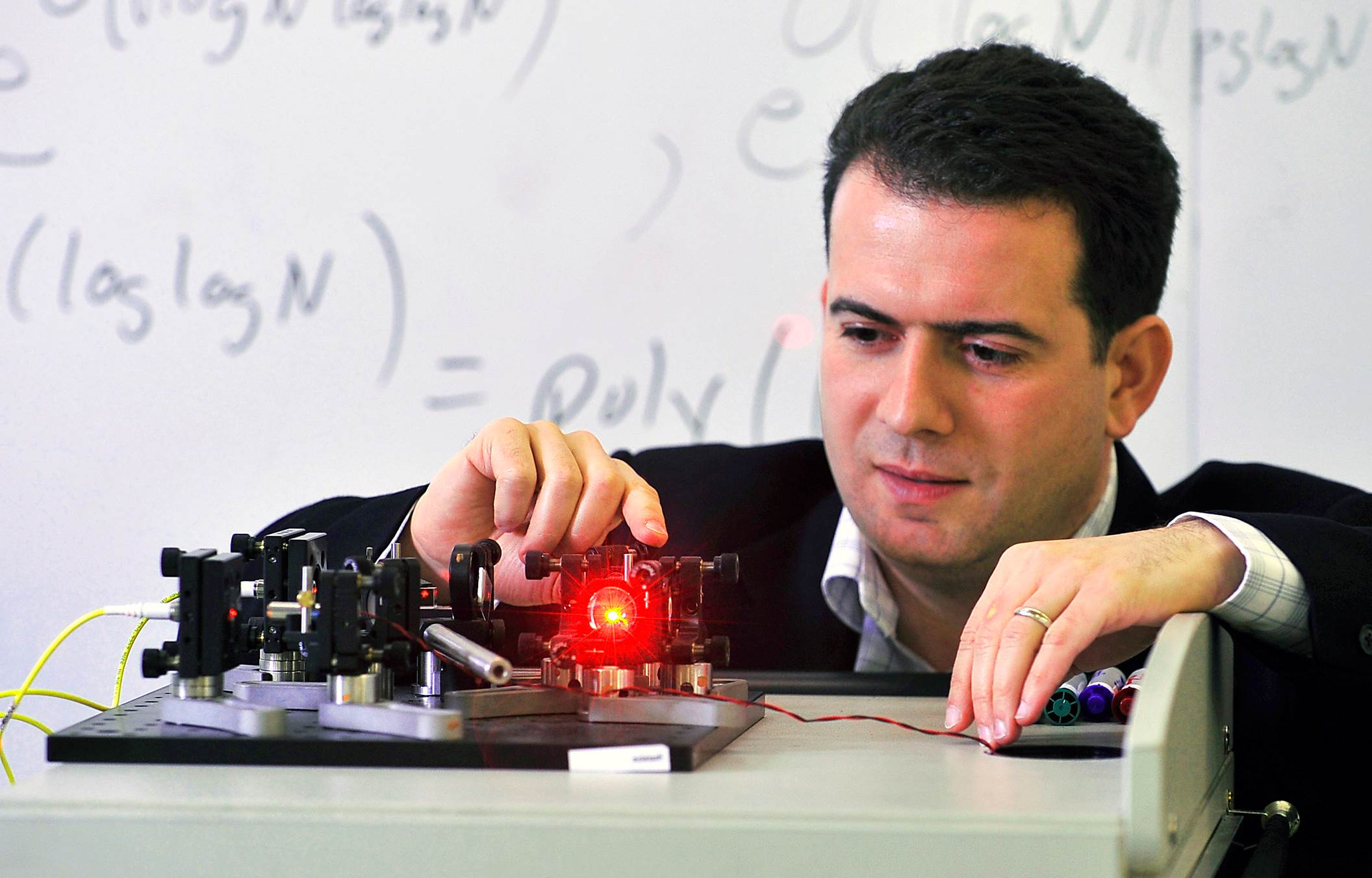 Professor Michele Mosca
Protecting financial data has always been a cat-and-mouse game. What is different now is that the cat could be de-clawed. Quantum computing, a new form of computer processing, promises to break open the security systems that safeguard much of the world’s financial data and transactions.
Quantum computing is expected to be much more powerful than anything currently available because it does not rely on the binary digits 1 or 0 to represent data but exploits the fact that subatomic particles can exist in more than one state at once.
Experts cannot say with certainty when a fully-fledged quantum computer will exist but, once it does, public key encryption schemes in use today will be breakable. Quantum computer algorithms that can crack such schemes have already been put through their paces.
The good news is that cryptographic techniques resilient to quantum computers exist. And while such “quantum-safe” technologies still need to be constructed, security experts agree that financial institutions must prepare now for a quantum-computer world.
Experts cannot say with certainty when a fully-fledged quantum computer will exist but, once it does, public key encryption schemes in use today will be breakable
Ticking clock
There is a 50 percent chance that a quantum computer will exist by 2031, according to Professor Michele Mosca, co-founder of the Institute for Quantum Computing at the University of Waterloo, Canada, and of security company evolutionQ.
A one-in-two chance of a fully working quantum computer by 2031 suggests financial institutions have time to prepare, but that is not the case. Since financial companies are required to keep data confidential for many years, quantum-safe protocols need to be in place for the same length of time that confidentiality is mandated prior to quantum computing. So, for example, if data must be kept confidential for seven years, quantum-safe techniques need to be in place by 2024 at the latest. Otherwise, cyber criminals need only intercept and store RSA-encrypted data after 2024 and wait until 2031 to have a 50-50 chance of access to sensitive information.
Unsurprisingly, replacing public key infrastructure with quantum-safe technology is itself a multi-year project. First, the new systems must be tested and verified to ensure they meet existing requirements – not just that their implementation is secure but that their execution times for various applications are satisfactory. Then, all the public key infrastructure needs to be revamped – a considerable undertaking. This means that, if upgrading infrastructure takes five years, companies should be preparing if quantum computers arrive by 2031.
Professor Renato Renner, the head of the quantum information theory research group at ETH Zurich, the Swiss science and technology university, sees the potential for even more immediate risk. “Having a full-blown quantum computer is not necessarily what you need to break cryptosystems,” he says. In his view, financial companies should be worried that there are already early examples of quantum computers that are stronger than current computers. “It could well be that in five years we have already sufficiently powerful devices that can break RSA cryptosystems,” says Renner.
Quantum-safe approaches
Quantum-safe technologies comprise two approaches, one based on maths and another that exploits the laws of physics.
The maths approach delivers new public key algorithms that are designed to be invulnerable to quantum computing, known as post-quantum or quantum-resistant techniques.
The US National Institute of Science and Technology is taking submissions for post-quantum algorithms with the goal of standardising a suite of protocols by the early to mid-2020s. These include lattice-based, coding-based, isogenies-based and hash-function-based schemes. The maths behind these schemes is complex but the key is that none of them is based on the multiplication of prime numbers and hence susceptible to factoring, which is what quantum computers excel at.
It could well be that in five years we have already sufficiently powerful devices that can break RSA cryptosystems
Nigel Smart, co-founder of Dyadic Security, a software-defined cryptography company, points out that companies are already experimenting with post-quantum lattice schemes. Earlier this year, Google used it in experimental versions of its Chrome browser when talking to its sites. “My betting is that lattice-based systems will win,” says Smart.
The other quantum-safe approach exploits the physics of the very small – quantum mechanics – to secure links so that an eavesdropper on the link cannot steal data. Here particles of light – photons – are used to send the key used to encrypt data (see Cryptosystems – two ways to secure data below) where each photon carries a digital bit of the key.
Financial and other companies that secure data should already be assessing the vulnerabilities of their security systems
Should an adversary eavesdrop with a photodetector and steal the photon, the photon will not arrive at the other end. Should the hacker be more sophisticated and try to measure the photon before sending it on, here they come up against the laws of physics where measuring a photon changes its parameters.
Given these physical properties of photons, the sender and receiver typically reserve at random a number of the key’s photons to detect a potential eavesdropper. If the receiver detects an altered photon, the change suggests the link is compromised.
But quantum key distribution only solves a particular class of problem – for example, protecting data sent across links such as a bank sending information to a data centre for back-up. Moreover, the distances a single photon can travel is a few tens of kilometres. If longer links are needed, intermediate trusted sites are required to regenerate the key, which is expensive and cumbersome.
The technique is also dependent on light and so is not as widely applicable as quantum-resistant techniques. “People are more interested in post-quantum cryptography,” claims Smart.
What now?
BT, working with Toshiba and ADVA Optical Networking, the optical transport equipment maker, has demonstrated a quantum-protected link operating at 100 gigabits-per-second.
What is missing still is a little bit more industrialisation,” says Andrew Lord, head of optical communications at BT. “Quantum physics is pretty sound but we still need to check that the way this is implemented, there are no ways of breaching it.”
 Kelly Richdale
ID Quantique, the Swiss quantum-safe crypto technology company, supplied one early-adopter bank with its quantum key distribution system as far back as 2007. The bank uses a symmetric key scheme coupled with a quantum key.
“You can think of it as adding an additional layer of quantum security on top of everything you already have,” says Kelly Richdale, ID Quantique’s vice-president of quantum-safe security.
“Quantum key distribution has provable security. You know it will be safe against a quantum computer if implemented correctly,” she says. “With post-quantum algorithms, it is a race against time, since in the future there may be new quantum attacks that could render them as vulnerable as RSA.”
Andersen Cheng, chief executive of start-up PQ Solutions, a security company with products including secure communication using post-quantum technology, argues that both quantum- resistant and quantum key distribution will be needed. “You can use both but quantum key distribution on its own is not enough and it is expensive,” he says.
Most organisations do not have a detailed map of where all their information assets are and which business functions rely on which crypto algorithms
What next?
Mosca says that leading financial services companies are aware of the threat posed by quantum computing but their strategies vary: some point to more pressing priorities while others want to know what they can buy now to solve the problem.
He disagrees with both extreme approaches. Financial companies should, in his view, already be assessing the vulnerabilities of their systems. “Most organisations do not have a detailed map of where all their information assets are and which business functions rely on which crypto algorithms,” he says.
Companies should also plan for their systems to change a lot over the next decade. That is why it is premature to settle on a solution now since it will probably need upgrading. And they must test quantum-resistant algorithms. “We don’t have a winner yet,” says Mosca.
Most importantly, financial institutions cannot afford to delay. “Do you really want to be in the catch-up game and hope someone else will solve the problem for you?” asks Mosca.
The article first appeared in the June-July issue of the Financial World, the journal of The London Institute of Banking & Finance, published six times per year in association with the Centre for The Study of Financial Innovation (CSFI).
Cryptosystems – two ways to secure data
To secure data, special digital “keys” are used to scramble the information. Two encryption schemes are used – based on asymmetric and symmetric keys.
Public key cryptography that uses a public and private key pair is an example of an asymmetric scheme. The public key, as implied by the name, is published with the user’s name. Any party wanting to send data securely to the user employs the published public key to scramble the data. Only the recipient, with the associated private key, can decode the sent data. The RSA algorithm is a widely used example. (RSA stands for the initials of the developers: Ron Rivest, Adi Shamir and Leonard Adleman.) A benefit of public key cryptography is that it can be used as a digital signature scheme as well as for protecting data. The downside is that it requires a lot of processing power and is slow even then.
Symmetric schemes, in contrast, are much less demanding to run and use the same key at both link ends to lock and unlock the data. A well-known symmetric key algorithm is the Advanced Encryption Standard, which uses keys up to 256-bits long (AES-256); the more bits, the more secure the encryption.
The issue with the symmetrical scheme is getting the secret key to the recipient without it being compromised. One way is to send a security guard handcuffed to a locked case. A more digital-age approach is to send the secret key over a secure link. Here, public key cryptography can be used; the asymmetric key scheme can be employed to protect the symmetric key transmission prior to secure symmetric communication.
Quantum computing is a potent threat because it undermines both schemes when existing public key cryptography is involved.
Elenion's coherent and fibre-to-the-server plans
- Elenion’s coherent chip - an integrated modulator-receiver assembly - is now generally available.
- The company has a silicon photonics design library that includes over 1,000 elements.
- Elenion is also developing an optical engine for client-side interfaces.
Elenion Technologies has given an update on its activities and strategy after announcing itself eight months ago. The silicon photonics-based specialist is backed by private equity firm, Marlin Equity Partners, which also owns systems vendor, Coriant. Elenion had already been active for two and a half years and shipping product when it emerged from its state of secrecy last December.
 Larry SchwerinElenion has since announced it is selling its telecom product, a coherent transceiver PIC, to Coriant and now other companies.
It has also progressed its optical engine design for the data centre that will soon be a product. Elenion has been working with Ethernet switch chip maker, Cavium, and data centre player, Microsoft, as part of its datacom work.
“We have moved forward,” says Larry Schwerin, the CEO of Elenion.
Coherent PIC
Elenion’s integrated modulator-receiver assembly is being used by Coriant for two CFP2 Analogue Coherent Optics (CFP2-ACO) modules as part of its Groove G30 platform.
The first is a short-reach CFP2-ACO for point-to-point 200-gigabit links that has a reach of at least 80km. The second is a high-performance CFP2-ACO that has a reach of up to 4,000km at 100 gigabits and 650km at 200 gigabits.
Schwerin says the company is now selling the coherent PIC to “a lot of people”. In addition to the CFP2-ACO, there is the Digital Coherent Optics (DCO) pluggable market where the PIC and the coherent digital signal processor (DSP) are integrated within the module. Examples include the CFP-DCO and the smaller CFP2-DCO which is now being designed into new systems. ADVA Optical Networking is using the CFP2-DCO for its Teraflex, as is its acquisition target MRV with its 200-gigabit coherent muxponder. Infinera’s latest XTM II platforms also use the CFP2-DCO.
We have got a library that has well over 1,000 elements
Using silicon photonics benefits the cost and performance of the coherent design, says Schwerin. The cost benefit is a result of optical integration. “You can look at it as a highly simplified supply chain,” says Schwerin. Coupling the electronics close to the optics also optimises overall performance.
Elenion is also targeting the line-card market for its coherent PIC. “This is one of the reasons why I wanted to stay out of the pluggable business,” says Schwerin. “There are a lot more customers out there if you stay out of pluggables because now you are selling an [optical] engine.”
The company is also developing a coherent PIC design that will support higher data rates such as 400- and 600-gigabit per lambda. “Without being too specific because we do remain stealthy, we have plans to support these applications,” says Schwerin.
Schwerin stresses that the real strength of the company is its design library used to develop its silicon photonics circuits. Elenion emerged out of a silicon photonics design-for-service company. “We have got a library that has well over 1,000 elements,” he says. Elenion says it can address custom design requests of companies using its design library.
Datacom
Elenion announced at the OFC show held in Los Angeles in March that it is working with Jabil AOC Technologies, a subsidiary of the manufacturing firm, Jabil Circuits. Elenion chose the contract manufacturer due to its ability to address both line-card and pluggable designs, the markets for its optical engines.
The two firms have also been working at the chip level on such issues as fibre attach, coupling the laser and adding the associated electronics. “We are trying to make the interface as elegant and streamlined as possible,” says Schwerin. “We have got initiatives underway so that you don't need these complex arrangements.”
Schwerin highlights the disparity between the unit volumes needed for the telecom and datacom markets. According to forecasts from market research firms, the overall coherent market is expected to grow to 800,000 and 1 million units a year by 2020. In contrast, the interfaces used inside one large-scale data centre can be up to 2 million. “To achieve rapid manufacturing and yield, you have got to simplify the process,” he says.
This is what Elenion is tackling. If 1,000 die can be made on a single silicon wafer, and knowing the interface volumes required and the yields, the total number of wafer runs can be determined. And it is the overall time taken from starting a wafer to the finished transceiver PIC output that Elenion is looking to shorten, says the CEO.
We ran that demo from 7 AM to 2 AM every day of the show
At OFC, Elenion hired a hotel suite near the convention centre to demonstrate its technologies to interested companies. One demonstration used its 25Gbps optical engine directly mounted on a Cavium QLogic network interface card (NIC) connecting a server to a high-capacity Cavium Xpliant Ethernet switch chip. The demo showed how 16 NICs could be connected to the switch chip for a total capacity of 400 gigabits. “No more direct-attached cables or active optical cables, literally fibre-to-the-server,” says Schwerin. “We ran that demo from 7 AM to 2 AM every day of the show.”
Elenion’s on-board optics design was based on the emerging Consortium of On-Board Optics (COBO) standard. “The Microsoft folks, we work with them closely, so obviously what we are doing follows their intent,” says Schwerin.
The optical engine will also support 56Gbps links when used with four-level pulse-amplitude modulation (PAM-4) and the company is even eyeing 100Gbps interfaces. For now, Elenion’s datacom optical engine remains a technical platform but a product will soon follow.
The company’s datacom work is also benefiting its telecom designs. “The platform technology that we use for datacom has now found its way into the coherent programme, especially around the packaging,” says Schwerin.
* The article was changed on July 25th to mention that Elenion's PIC is being used in two Coriant CFP-ACOs.
Silicon photonics: concerns but viable and still evolving
Blaine Bateman set himself an ambitious goal when he started researching the topic of silicon photonics. The president of the management consultancy, EAF LLC, wanted to answer some key questions for a broad audience, not just academics and researchers developing silicon photonics but executives working in data centres, telecom and IT.
The result is a 192-page report entitled Silicon Photonics: Business Situation Report, 59 pages alone being references. In contrast to traditional market research reports, there is also no forecast or company profiles.
 Blaine Bateman's risk meter for silicon photonics. Eleven key elements needed to deploy a silicon photonics solution were considered. And these were assessed from the perspective of various communities involved or impacted by the technology, from silicon providers to cloud-computing users. Source: EAF LLC.
“I thought it would be helpful to give people a business view,” says Bateman.
Bateman works with companies on strategy in such areas as antennas, wireless technologies and more recently analytics and machine learning. But a growing awareness of photonics made him want to research the topic. “I could see a convergence between the evolution of telecom switching centres to become more like data centres, and data centres starting to look more like telecoms,” he says.
The attraction of silicon photonics is that it is an emerging technology with wide applicability in communications.
Just watching entirely new technologies emerge and become commercially viable in the span of ten years; it is astonishing
“Silicon Photonics is a good topic to research and publish to help a broader community because it is highly technical,” says Bateman. “It is also a great case study, just watching entirely new technologies emerge and become commercially viable in the span of ten years; it is astonishing.”
Bateman spent two years conducting interviews and reading a vast number of academic papers and trade-press articles before publishing the report earlier this year.
 Blaine BatemanThe main near-term opportunity for silicon photonics he investigated is the data centre. Moreover, not just large-scale data centre players with an obvious need for cheaper optics to interconnect servers but also enterprises facing important decisions regarding their cloud-computing strategy.
“The view that I developed is that it is still very early,” he says. “The price points for a given performance [of optics] are significantly higher than a Facebook thinks they need to meet their long-term business perspectives.”
The price-performance figure commonly floated is one dollar per gigabit but current 100-gigabit pluggable modules, whether using indium phosphide or silicon photonics, are several times more costly than that.
This is an important issue for cloud providers and for enterprises determining their cloud strategy.
Do cloud provider invest money in silicon photonics technologies for their data centres or do they let others be early adopters and come in later when prices have dropped? Equally, an enterprise considering moving their business operations to the cloud is in a precarious position, says Bateman. “If you pick the wrong horse, you could be boxed into a level of price and performance, while you will have competitors starting with cloud providers that have a 30 to 50 percent price-performance advantage,” he says. “In my view, it will trickle all the way to the large consumers of cloud resources.”
Longer term, the market will resolve the relative success of silicon photonics versus traditional optics but, near term, companies have some expensive decisions to make. “The price curve is still in the early phase,” says Bateman. “It just hasn’t come down enough that it is an easy decision.”
Bateman’s advice to enterprises considering a potential cloud provider is to ask about its roadmap plans regarding the deployment of photonics.
Findings
To help understand the technology and business risks associated with silicon photonics, Bateman has created risk meters. These are intuitive graphics that show the status of the different elements making up silicon photonics and the issues involved when making silicon phonics devices. These include the light source, modulation method, formation of the waveguides, fibering the chip and fabrication plants.
“The reason the fab is such a high risk is that even though the idea was to leverage existing foundries, in truth it is very much new processes,” says Bateman. “There is also a limited number of fabs that can build these things.”
The report also includes a risk meter summarising the overall status of silicon photonics (see above).
Bateman says there are concerns regarding silicon photonics which people need to be aware of but stresses that it is a viable technology.
This is one of two main conclusions he highlights. Silicon photonics is not mature enough to be at a commodity price. Accordingly, taking a non-commodity or early adopter technology could damage a company’s business plan in terms of cost and performance.
The second takeaway is that for every single aspect of silicon photonics, much is still open. “One of the reasons I made all these lists in the report - and I studied research from all over the globe - is that I wanted to show the management level that silicon photonics is still emerging,” says Bateman.
China is focused on innovation now, and has formidable resources
This surprised him. When a new technology comes to market, it typically uses R&D developed decades earlier. “In this area, I was shocked by the huge amount of basic research this is still ongoing and more and more is being done every day,” says Bateman. “It is daunting; it is moving so fast.”
Another aspect that surprised him was the amount of research coming out of Asia and in particular China. “This is also something new, seeing original work in China and other parts of the world,” he says.
The stereotypical view that China is a source of cheap manufacturing but little in terms of innovation must change, he says. In the US, in particular, there is still a large body of people that think this way, says Bateman: “I feel they have their head in the sand - China is focused on innovation now, and has formidable resources.”
The era of cloud-scale routeing
 Nokia's FP4 p-chip. The multi-chip module shows five packages: the p-chip die surrounded by four memory stacks. Each stack has five memory die. The p-chip and memory stacks are interconnected using an interposer.
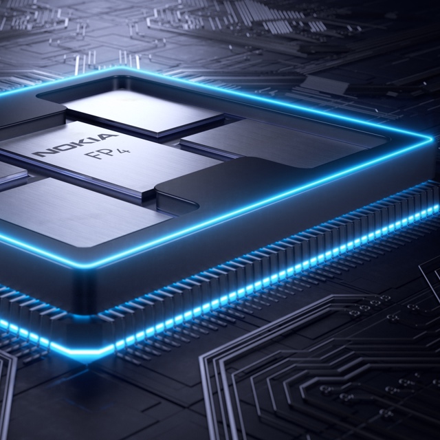
 - Nokia has unveiled the FP4, a 2.4 terabit-per-second network processor that has 6x the throughput of its existing FP3.
- The FP4 is a four-IC chipset implemented using 16nm CMOS FinFET technology. Two of the four devices in the chipset are multi-chip modules.
- The FP4 uses 56 gigabit-per-second serial-deserialiser (serdes) technology from Broadcom, implemented using PAM-4 modulation. It also supports terabit flows.
- Nokia announced IP edge and core router platforms that will use the FP4, the largest configuration being a 0.58 petabit switching capacity router.
Much can happen in an internet minute. In that time, 4.1 million YouTube videos are viewed, compared to 2.8 million views a minute only last year. Meanwhile, new internet uses continue to emerge. Take voice-activated devices, for example. Amazon ships 50 of its Echo devices every minute, almost one a second.
Given all that happens each minute, predicting where the internet will be in a decade’s time is challenging. But that is the task Alcatel-Lucent’s (now Nokia’s) chip designers set themselves in 2011 after the launch of its FP3 network processor chipset that powers its IP-router platforms.
Six years on and its successor - the FP4 - has just been announced. The FP4 is the industry’s first multi-terabit network processor that will be the mainstay of Nokia’s IP router platforms for years to come.
Cloud-scale routing
At the FP4’s launch, Nokia’s CEO, Rajeev Suri, discussed the ‘next chapter’ of the internet that includes smart cities, new higher-definition video formats and the growing number of connected devices.
IP traffic is growing at a compound annual growth rate (CAGR) of 25 percent through to 2022, according to Nokia Bell Labs, while peak data rates are growing at a 39 percent CAGR. Nokia Bell Labs also forecasts that the number of connected devices will grow from 12 billion this year to 100 billion by 2025.
Basil Alwan, Nokia’s president of IP and optical networks, said the internet has entered the era of cloud-scale routeing. When delivering a cloud service, rarely is the request fulfilled by one data centre. Rather, several data centres are involved in fulfilling the tasks. “One transaction to the cloud is multiplied,” said Alwan.
IP traffic is also becoming more dynamic, while the Internet of Things presents a massive security challenge.
Alwan also mentioned how internet content providers have much greater visibility into their traffic whereas the telcos’ view of what flows in their networks is limited. Hence their interest in analytics to understand and manage their networks better.
These are the trends that influenced the design of the FP4.
We put a big emphasis on making sure we had a high degree of telemetry coming out at the chip level
FP4 goals
Telemetry, the sending of measurement data for monitoring purposes, and network security were two key design goals for the FP4.
 Steve Vogelsang“We put a big emphasis on making sure we had a high degree of telemetry coming out at the chip level,” said Steve Vogelsang, CTO for Nokia's IP and optical business.
Tasks include counters, collecting statistics and packet copying. “This is to make sure we have the instrumentation coming off these systems that we can use to drive the [network] analytics platform,” said Vogelsang.
Being able to see the applications flowing in the network benefits security. Distributed Denial-of-Service (DDoS) attacks are handled by diverting traffic to a ‘scrubbing centre’ where sophisticated equipment separates legitimate IP packets from attack traffic that needs scrubbing.
The FP4 supports the deeper inspection of packets. “Once we identify a threat, we can scrub that traffic directly in the network,” said Vogelsang. Nokia claims that that the FP4 can deal with over 90 percent of the traffic that would normally go to a scrubbing centre.
Chipset architecture
Nokia’s current FP3 network processor chipset comprises three devices: the p-chip network processor, the q-chip traffic manager and the t-chip fabric interface device.
The p-chip network processor inspects packets and performs table look-ups using fast-access memory to determine where packets should be forwarded. The q-chip is the traffic manager that oversees the packet flows and decides how packets should be dealt with, especially when congestion occurs. The third FP3 chip is the t-chip that interfaces to the router fabric.
The FP4 retains the three chips and adds a fourth: the e-chip - a media access controller (MAC) that parcels data from the router’s client-side pluggable optical modules for the p-chip. However, while the FP4 retains the same nomenclature for the chips as the FP3, the CMOS process, chip architecture and packaging used to implement the FP4 are significantly more advanced.
The FP4 can deal with over 90 percent of the traffic that would normally go to a scrubbing centre
Nokia is not providing much detail regarding FP4 chipset's architecture, unlike the launch of the FP3. “We wanted to focus on the re-architecture we have gone through,” said Vogelsang. But looking at the FP3 design, insight can be gained as to how the FP4 has likely changed.
The FP3’s p-chip uses 288 programmable cores. Each programmable core can process two instructions each clock cycle and is clocked at 1GHz.
The 288 cores are arranged as a 32-row-by-9-column array. Each row of cores can be viewed as a packet-processing pipeline. A row pipeline can also be segmented to perform independent tasks. The array’s columns are associated with table look-ups. The resulting FP3 p-chip is a 400-gigabit network processor.
Vogelsang said there is limited scope to increase the clock speed of the FP4 p-chip beyond 1GHz. Accordingly, the bulk of the FP4’s sixfold throughput improvement is the result of a combination of programmable core enhancements, possible a larger core array and, most importantly, system improvements. In particular, the memory architecture is now packaged within the p-chip for fast look-ups, while the chipset’s input-output lanes have been boosted from 10 gigabits-per-second (Gbps) to 50Gbps.
Nokia has sought to reuse as much of the existing microcode to program the cores for the FP4 p-chip but has added new instructions to take advantage of changes in the pipeline.
Software compatibility already exists at the router operating system level. The same SROS router operating system runs on Nokia’s network processors, merchant hardware from the like of Broadcom and on x86 instruction-set microprocessors in servers using virtualisation technology.
Such compatibility is achieved using a hardware abstraction layer that sits between the operating system and the underlying hardware. “The majority of the software we write has no idea what the underlying hardware is,” said Vogelsang.
Nokia has a small team of software engineers focussed on the FP4’s microcode changes but, due to the hardware abstraction layer, such changes are transparent to the main software developers.
The FP3’s traffic manager, the q-chip, comprises four reduced instruction set computer (RISC) cores clocked at 900MHz. This too has been scaled up for the FP4 but Nokia has not given details.
The t-chip interfaces to the switch fabric that sits on a separate card. In previous generations of router products, a mid-plane is used, said Nokia. This has been scrapped with the new router products being announced. Instead, the switch cards are held horizontally in the chassis and the line cards are vertical. “A bunch of metal guides are used to guide the two cards and they directly connect to each other,” said Vogelsang. “The t-chips are what interface to these connectors inside the system.”
The MAC e-chip interfaces to the line card’s pluggable modules and support up to a terabit flow. Indeed, the MAC will support integer multiples of 100 Gigabit Ethernet from 100 gigabit to 1 terabit. Nokia has a pre-standard implementation of FlexMAC that allows it to combine lanes across multiple transceivers into a single interface.
Nokia will have line cards that support 24 or 36 QSFP-DD pluggable modules, with each module able to support 400 Gigabit Ethernet.
The FP4 is also twice as power efficient, consuming 4 gigabit/W.
We wanted to make sure we used a high-volume chip-packaging technology that was being driven by other industries and we found that in the gaming industry
Design choices
One significance difference between the two network processor generations is the CMOS process used. Nokia skipped 28nm and 22nm CMOS nodes to go from 40nm CMOS for the FP3 to 16nm FinFET for the FP4. “We looked at that and we did not see all the technologies we would need coming together to get the step-function in performance that we wanted,” said Vogelsang.
Nokia also designed its own memory for the FP4.
“A challenge we face with each generation of network processor is finding memories and memory suppliers that can offer the performance we need,” said Vogelsang. The memory Nokia designed is described as intelligent: instructions can effectively be implemented during memory access and the memory can be allocated to do different types of look-up and buffering, depending on requirements.
Another key area associated with maximising the performance of the memory is the packaging. Nokia has adopted multi-chip module technology for the p-chip and the q-chip.
“We wanted to make sure we used a high-volume chip-packaging technology that was being driven by other industries and we found that in the gaming industry,” said Vogelsang, pointing out that the graphics processing unit (GPU) has similar requirements to those of a network processor. GPUs are highly memory intensive while manipulating bits on a screen is similar to manipulating headers and packets.
The resulting 2.5D packaged p-chip comprises the packet processor die and stacks of memory. Each memory stack comprises 5 memory die. All sit on an interposer substrate - itself a die that is used for dense interconnect of devices. The resulting FP4 p-chip is thus a 22-die multi-chip module.
“Our memory stacks are connected at the die edges and do not use through-silicon vias,” said Vogelsang. “Hence it is technically a 2.5D package [rather than 3D].”
The q-chip is also implemented as a multi-chip module containing RISC processors and buffering memory, whereas the router fabric t-chip and MAC e-chip are single-die ICs.
The FP4’s more advanced CMOS process also enables significantly faster interfaces. The FP4 uses PAM-4 modulation to implement 56Gbps interfaces. “You really need to run those bit rates much much higher to get the traffic into and out of the chip,” said Vogelsang.
Nokia says it is using embedded serialiser-deserialiser interface technology from Broadcom.
Next-gen routers
Nokia has also detailed the IP edge and core routers that will use the FP4 network processor.
The 7750 Service Router (SR-s) edge router family will support up to 144 terabits in a single shelf. This highest capacity configuration is the 7750 SR-14. It is a 24-rack-unit-plus-the-power-supply high chassis and supports a dozen line cards, each 12Tbps when using 100-gigabit modules, or 24x400GbE when using QSFP-DD modules.
Another new platform is the huge 7950 Extensible Routing System (XRS-XC) IP core router which can be scaled to 576 terabits - over half a petabit - when used in a six-chassis configuration. Combining the six chassis does not make require the use of front-panel client-side interfaces. Instead, dedicated interfaces are used with active optical cables to interlink the chassis.
The first router products will be shipped to customers at the year end with general availability expected from the first quarter of 2018.
Meeting the many needs of data centre interconnect
High capacity. Density. Power efficiency. Client-side optical interface choices. Coherent transmission. Direct detection. Open line system. Just some of the requirements vendors must offer to compete in the data centre interconnect market.
“A key lesson learned from all our interactions over the years is that there is no one-size-fits-all solution,” says Jörg-Peter Elbers, senior vice president of advanced technology, standards and IPR at ADVA Optical Networking. “What is important is that you have a portfolio to give customers what they need.”
 Jörg-Peter Elbers
Teraflex
ADVA Optical Networking detailed its Teraflex, the latest addition to its CloudConnect family of data centre interconnect products, at the OFC show held in Los Angeles in March (see video).
The platform is designed to meet the demanding needs of the large-scale data centre operators that want high-capacity, compact platforms that are also power efficient.
A key lesson learned from all our interactions over the years is that there is no one-size-fits-all solution
Teraflex is a one-rack-unit (1RU) stackable chassis that supports three hot-pluggable 1.2-terabit modules or ‘sleds’. A sled supports two line-side wavelengths, each capable of coherent transmission at up to 600 gigabits-per-second (Gbps). Each sled’s front panel supports various client-side interface module options: 12 x 100-gigabit QSFPs, 3 x 400-gigabit QSFP-DDs and lower speed 10-gigabit and 40-gigabit modules using ADVA Optical Networking’s MicroMux technology.
“Building a product optimised only for 400-gigabit would not hit the market with the right feature set,” says Elbers. “We need to give customers the possibility to address all the different scenarios in one competitive platform.”
The Teraflex achieves 600Gbps wavelengths using a 64-gigabaud symbol rate and 64-ary quadrature-amplitude modulation (64-QAM). ADVA Optical Networking is using Acacia’s Communications latest Pico dual-core coherent digital signal processor (DSP) to implement the 600-gigabit wavelengths. ADVA Optical Networking would not confirm Acacia is its supplier but Acacia decided to detail the Pico DSP at OFC because it wanted to end speculation as to the source of the coherent DSP for the Teraflex. That said, ADVA Optical Networking points out that Teraflex’s modular nature means coherent DSPs from various suppliers can be used.
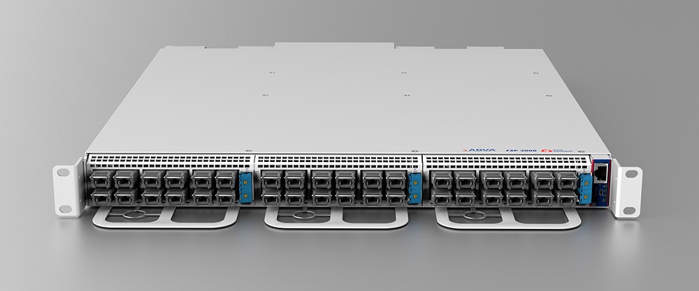 The 1 rack unit Teraflex
The line-side optics supports a variety of line speeds – from 600Gbps to 100Gbps, the lower the speed, the longer the reach.
The resulting 3-sled 1RU Teraflex platform thus supports up to 3.6 terabits-per-second (Tbps) of duplex communications. This compares to a maximum 800Gbps per rack unit using the current densest CloudConnect 0.5RU Quadflex card.
Markets
The data centre interconnect market is commonly split into metro and long haul.
The metro data centre interconnect market requires high-capacity, short-haul, point-to-point links up to 80km. Large-scale data centre operators may have several sites spread across a city, given they must pick locations where they can find them. Sites are typically no further apart than 80km to ensure a low-enough latency such that, collectively, they appear as one large logical data centre.
“You are extending the fabric inside the data centre across the data-centre boundary, which means the whole bandwidth you have on the fabric needs to be fed across the fibre link,” says Elbers. “If not, then there are bottlenecks and you are restricted in the flexibility you have.”
Large enterprises also use metro data centre interconnect. The enterprises’ businesses involve processing customer data - airline bookings, for example - and they cannot afford disruption. As a result, they may use twin data centres to ensure business continuity.
Here, too, latency is an issue especially if synchronous mirroring of data using Fibre Channel takes place between sites. The storage protocol requires acknowledgement between the end points such that the round-trip time over the fibre is critical. “The average distance of these connections is 40km, and no one wants to go beyond 80 or 100km,” says Elbers, who stresses that this is not an application for Teraflex given it is aimed at massive Ethernet transport. Customers using Fibre Channel typically need lower capacities and use more tailored solutions for the application.
The second data centre interconnect market - long haul - has different requirements. The links are long distance and the data sent between sites is limited to what is needed. Data centres are distributed to ensure continual business operation and for quality-of-experience by delivering services closer to customers.
Hundreds of gigabits and even terabits are sent over the long-distance links between data centres sites but commonly it is about a tenth of the data sent for metro data centre interconnect, says Elbers.
Direct Detection
Given the variety of customer requirements, ADVA Optical Networking is pursuing direct-detection line-side interfaces as well as coherent-based transmission.
At OFC, the system vendor detailed work with two proponents of line-side direct-detection technology - Inphi and Ranovus - as well as its coherent-based Teraflex announcement.
Working with Microsoft, Arista and Inphi, ADVA detailed a metro data centre interconnect demonstration that involved sending 4Tbps of data over an 80km link. The link comprised 40 Inphi ColorZ QSFP modules. A ColorZ module uses two wavelengths, each carrying 56Gbps using PAM-4 signalling. This is where having an open line system is important.
Microsoft wanted to use QSFPs directly in their switches rather than deploy additional transponders, says Elbers. But this still requires line amplification while the data centre operators want the same straightforward provisioning they expect with coherent technology. To this aim, ADVA demonstrated its SmartAmp technology that not only sets up the power levels of the wavelengths and provides optical amplification but also automatically measures and compensates for chromatic dispersion experienced over a link.
ADVA also detailed a 400Gbps metro transponder card based on PAM-4 implemented using two 200Gbps transmitter optical subassemblies (TOSAs) and two 200Gbps receiver optical subassemblies (ROSAs) from Ranovus.
Clearly there is also space for a direct-detection solution but that space will narrow down over time
Choices
The decision to use coherent or direct detection line-side optics boils down to a link’s requirements and the cost an end user is willing to pay, says Elbers.
As coherent-based optics has matured, it has migrated from long-haul to metro and now data centre interconnect. One way to cost-reduce coherent further is to cram more bits per transmission. “Teraflex is adding chunks of 1.2Tbps per sled which is great for people with very high capacities,” says Elbers, but small enterprises, for example, may only need a 100-gigabit link.
“For scenarios where you don’t need to have the highest spectral efficiency and the highest fibre capacity, you can get more cost-effective solutions,” says Elbers, explaining the system vendor’s interest in direct detection.
“We are seeing coherent penetrating more and more markets but still cost and power consumption are issues,” says Elbers. “Clearly there is also space for a direct-detection solution but that space will narrow down over time.”
Developments in silicon photonics that promise to reduce the cost of optics through greater integration and the adoption of packaging techniques from the CMOS industry will all help. “We are not there yet; this will require a couple of technology iterations,” says Elbers.
Until then, ADVA’s goal is for direct detection to cost half that of coherent.
“We want to have two technologies for the different areas; there needs to be a business justification [for using direct detection],” he says. “Having differentiated pricing between the two - coherent and direct detection - is clearly one element here.”
The OIF’s 400ZR coherent interface starts to take shape
Part 2: Coherent developments
The Optical Internetworking Forum’s (OIF) group tasked with developing two styles of 400-gigabit coherent interface is now concentrating its efforts on one of the two.
When first announced last November, the 400ZR project planned to define a dense wavelength-division multiplexing (DWDM) 400-gigabit interface and a single wavelength one. Now the work is concentrating on the DWDM interface, with the single-channel interface deemed secondary.
 Karl Gass"It [the single channel] appears to be a very small percentage of what the fielded units would be,” says Karl Gass of Qorvo and the OIF Physical and Link Layer working group vice chair, optical, the group responsible for the 400ZR work.
The likelihood is that the resulting optical module will serve both applications. “Realistically, probably both [interfaces] will use a tunable laser because the goal is to have the same hardware,” says Gass.
The resulting module may also only have a reach of 80km, shorter than the original goal of up to 120km, due to the challenging optical link budget.
Origins and status
The 400ZR project began after Microsoft and other large-scale data centre players such as Google and Facebook approached the OIF to develop an interoperable 400-gigabit coherent interface they could then buy from multiple optical module makers.
The internet content providers’ interest in an 80km-plus link is to connect premises across the metro. “Eighty kilometres is the magic number from a latency standpoint so that multiple buildings can look like a single mega data centre,” says Nathan Tracy of TE Connectivity and the OIF’s vice president of marketing.
Since then, traditional service providers have shown an interest in 400ZR for their metro needs. The telcos’ requirements are different to the data centre players, causing the group to tweak the channel requirements. This is the current focus of the work, with the OIF collaborating with the ITU.
The catch is how much can we strip everything down and still meet a large percentage of the use cases
“The ITU does a lot of work on channels and they have a channel measurement methodology,” says Gass. “They are working with us as we try to do some division of labour.”
The group will choose a forward error correction (FEC) scheme once there is common agreement on the channel. “Imagine all those [coherent] DSP makers in the same room, each one recommending a different FEC,” says Gass. “We are all trying to figure out how to compare the FEC schemes on a level playing field.”
Meeting the link budget is challenging, says Gass, which is why the link might end up being 80km only. “The catch is how much can we strip everything down and still meet a large percentage of the use cases.”
The cloud is the biggest voice in the universe
400ZR form factors
Once the FEC is chosen, the power envelope will be fine-tuned and then the discussion will move to form factors. The OIF says it is still too early to discuss whether the project will select a particular form factor. Potential candidates include the OSFP MSA and the CFP8.
 Nathan TracyThe industry assumption is that the 80km-plus 400ZR digital coherent optics module will consume around 15W, requiring a very low-power coherent DSP that will be made using 7nm CMOS.
“There is strong support across the industry for this project, evidenced by the fact that project calls are happening more frequently to make the progress happen,” says Tracy.
Why the urgency? “The cloud is the biggest voice in the universe,” says Tracy. To support the move of data and applications to the cloud, the infrastructure has to evolve, leading to the data centre players linking smaller locations spread across the metro.
“At the same time, the next-gen speed that is going to be used in these data centres - and therefore outside the data centres - is 400 gigabit,” says Tracy.
Coherent optics players target the network edge for growth
Part 1: Coherent developments
The market for optical links for reaches between 10km and 120km is emerging as a fierce battleground between proponents of coherent and direct-detection technologies.
Interest in higher data rates such as 400 gigabits is pushing coherent-based optical transmission from its traditional long-distance berth to shorter-reach applications. “That tends to be where the growth for coherent has come from as it has migrated from long-haul to metro,” says Tom Williams, senior director of marketing at Acacia Communications, a coherent technology supplier.
 Source: Acacia Communications, Gazettabyte
Williams points to the Optical Internetworking Forum’s (OIF) ongoing work to develop a 400-gigabit link for data centre interconnect. Dubbed 400ZR, the project is specifying an interoperable coherent interface that will support dense wavelength-division multiplexing (DWDM) links for distances of at least 80km.
Meanwhile, the IEEE standards group defining 400 Gigabit Ethernet has issued a Call-For-Interest to determine whether to form a Study Group to look at 400-Gigabit applications beyond the currently defined 10km 400GBASE-LR8 interface.
“Coherent moving to higher-volume, shorter-reach solutions shows it is not just a Cadillac product,” says Williams. Higher-volume markets will also be needed to fund coherent chip designs using advanced CMOS process nodes. “Seven nanometer [CMOS] becomes a very expensive prospect,” says Williams. “The traditional business case is not going to be there without finding higher volumes.”
Coherent moving to higher-volume, shorter-reach solutions shows it is not just a Cadillac product
Pico DSP
Acacia detailed its next-generation high-end coherent digital signal processor (DSP) at the OFC show held in Los Angeles in March.
 Tom WilliamsDubbed Pico, the DSP will support transmission speeds of up to 1.2 terabits-per-second using two carriers, each carrying 600 gigabits of data implemented using 64-ary quadrature amplitude modulation (64QAM) and a 64 gigabaud symbol rate. The 16nm CMOS dual-core DSP also features an internal crossbar switch to support a range of 100-gigabit and 400-gigabit client interfaces.
ADVA Optical Networking is using the Pico for its Teraflex data centre interconnect product. The Teraflex design supports 3.6 terabits of line-side capacity in a single rack unit (1RU). Each 1RU houses three “sleds”, each supporting two wavelengths operating at up to 600 gigabits-per-second (Gbps).
But ADVA Optical Networking also detailed at OFC its work with leading direct-detection technology proponents, Inphi and Ranovus. For the data centre interconnect market, there is interest in coherent and direct-detection technologies, says ADVA.
Detailing the Pico coherent DSP before it is launched as a product is a new development for Acacia. “We knew there would be speculation about ADVA’s Teraflex technology and we preferred to be up front about it,” says Williams.
The 16nm Pico chip was also linked to an Acacia post-deadline paper at OFC detailing the company’s progress in packaging its silicon photonics chips using ball grid array (BGA) technology. Williams stresses that process issues remain before its photonic integrated circuit (PIC) products will use BGA packaging, an approach that will simplify and reduce manufacturing costs.
“You are no longer running the board with all the electronics through a surface mount line and then have technicians manually solder on the optics,” says Williams. Moreover, BGA packaging will lead to greater signal integrity, an important consideration as the data rates between the coherent DSP and the PIC increase.
It is an endorsement of our model but I do not think it is the same as ours. You still have to have someone providing the DSP and someone else doing the optics
Coherent competition
Ciena's recent announcement that it is sharing its WaveLogic Ai coherent DSP technology with optical module vendors Lumentum, Oclaro and NeoPhotonics is seen as a response to Acacia’s success as a merchant supplier of coherent modules and coherent DSP technologies.
Williams says Acacia’s strategy remains the same when asked about the impact of the partnership between Ciena and the optical module makers: to continue being first to market with differentiated products.
One factor that has helped Acacia compete with merchant suppliers of coherent DSPs - NEL and ClariPhy, now acquired by Inphi - is that it also designs the silicon photonics-based optics used in its modules. This allows a trade-off between the DSP and the optics to benefit the overall system design.
A challenge facing the three optical module makers working with Ciena is that each one will have to go off and optimise their design, says Williams. “It is an endorsement of our model but I do not think it is the same as ours,” he says. “You still have to have someone providing the DSP and someone else doing the optics.”
Coherent roadmap
Acacia has managed to launch a new coherent DSP product every year since 2011 (see diagram, above). In 2015 it launched its Denali DSP, the first to operate at line rates greater than 100Gbps.
Last year it announced the Meru, a low-power DSP for its CFP2-DCO module. The CFP2-DCO operates at 100Gbps using polarisation multiplexing, quadrature phase-shift keying, (PM-QPSK) and two 200Gbps modes: one using 16-ary quadrature amplitude modulation (PM-16QAM) and a longer reach variant, implemented using a higher baud rate and 8-ary quadrature amplitude modulation (PM-8QAM). The CFP2-DCO is already starting to be designed into platforms.
Since 2014, Acacia has launched a low-power DSP design every even year and a high-end DSP every odd year, with the Pico being the latest example.
Acacia has not said when the Pico coherent DSP will be generally available but ADVA Optical Networking has said it expects to launch the Teraflex in early 2018.