
The many paths to 400 gigabits
The race is on to deliver 400-gigabit optical interfaces in time for the next-generation of data centre switches expected in late 2018.
The industry largely agrees that a four-wavelength 400-gigabit optical interface is most desirable yet alternative designs are also being developed.
Optical module makers must consider such factors as technical risk, time-to-market and cost when choosing which design to back.
 Rafik Ward, FinisarUntil now, the industry has sought a consensus on interfaces, making use of such standards bodies as the IEEE to serve the telecom operators.
Now, the volumes of modules used by the internet giants are such that they dictate their own solutions. And the business case for module makers is sufficiently attractive that they are willing to comply.
Another challenge at 400 gigabits is that there is no consensus regarding what pluggable form factor to use.
“There is probably more technical risk in 400 gigabits than any of the historical data-rate jumps we have seen,” says Rafik Ward, vice president of marketing at Finisar.
Shrinking timeframes
One-hundred-gigabit interfaces are now firmly established in the marketplace. It took several generations to achieve the desired module design. First, the CFP module was used, followed by the CFP2. The industry then faced a choice between the CFP4 and the QSFP28 form factors. The QSFP28 ended up winning because the 100-gigabit module met the price, density and performance expectations of the big users - the large-scale data centre players, says Paul Brooks, director of strategy for lab and production at Viavi Solutions.
“The QSFP28 is driving huge volumes, orders of magnitude more than we see with the other form factors,” he says.
There is probably more technical risk in 400 gigabits than any of the historical data-rate jumps we have seen
It was the telcos that initially drove 100-gigabit interfaces, as with all the previous interface speeds. Telcos have rigorous optical and physical media device requirements such that the first 100-gigabit design was the 10km 100GBASE-LR4 interface, used to connect IP routers and dense wavelength-division multiplexing (DWDM) equipment.
 Paul Brooks, Viavi Solutions
But 100 gigabits is also the first main interface speed influenced by the internet giants. “One-hundred-gigabit volumes didn’t take that inflection point until we saw the PSM4 and CWDM4 [transceiver designs],” says Brooks. The PSM4 and CWDM4 are not IEEE specification but multi-source agreements (MSAs) driven by the industry.
The large-scale data centre players are now at the forefront driving 400 gigabits. They don’t want to wait for three generations of modules before they get their hands on an optimised design. They want the end design from the start.
“There was a lot of value in having iterations at 100 gigabits before we got to the high-volume form factor,” says Ward. “It will be more challenging with the compressed timeframe for 400 gigabits.”
Datacom traffic is driven by machine-to-machine communication whereas telecom is driven by consumer demand. Machine-to-machine has twice the growth rate.
Data centre needs
Brandon Collins, CTO of Lumentum, explains that the urgency of the large-scale data centre players for 400 gigabits is due to their more pressing capacity requirements compared to the telcos.
 Brandon Collings, LumentumDatacom traffic is driven by machine-to-machine communication whereas telecom is driven by consumer demand. “Machine-to-machine has twice the growth rate,” says Collins. “The expectation in the market - and everything in the market aligns with this - is that the datacom guys will be adopting in volume much sooner than the telecom guys.”
The data centre players require 400-gigabit interfaces for the next-generation 6.4- and 12.8-terabit top-of-rack switches in the data centre.
“The reason why the top-of-rack switch is going to need 400-gigabit uplinks is because server speeds are going to go from 25 gigabits to 50 gigabits,” says Adam Carter, chief commercial operator for Oclaro.
A top-of-rack switch’s downlinks connect to the servers while the uplinks interface to larger ‘spine’ switches. For a 36-port switch, if four to six ports are reserved for uplinks and the remaining ports are at 50 gigabits-per-second (Gbps), 100-gigabit uplinks cannot accommodate all the traffic.
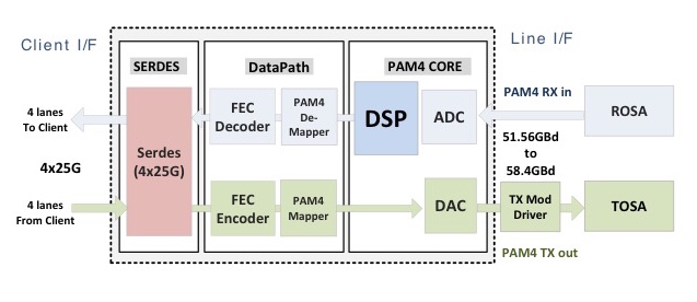
The 6.4-terabit and 12.8-terabit switches are expected towards the end of next year. These switches will be based on silicon such as Broadcom’s Tomahawk-III, start-up Innovium’s Teralynx and Mellanox’s Spectrum-2. All three silicon design examples use 50-gigabit electrical signalling implemented using 4-level pulse-amplitude modulation (PAM-4).
PAM-4, a higher order modulation scheme, used for the electrical and optical client interfaces is another challenge at 400-gigabit. The use of PAM-4 requires a slight increase in bandwidth, says Brooks, and introduces a loss that requires compensation using forward error correction (FEC). “Four-hundred-gigabits is the first Ethernet technology where you always have FEC on,” he says.
CFP8
The modules being proposed for 400-gigabit interfaces include the CFP8, the Octal Small Form Factor (OSFP) and the double-density QSFP (QSFP-DD) pluggable modules. COBO, the interoperable on-board optics standard, will also support 400-gigabit interfaces.
The QSFP-DD is designed to be backward compatible with the QSFP and QSFP28 pluggables while the OSFP is a new form factor.
At OFC earlier this year, several companies showcased 400-gigabit CFP8-based designs.
NeoPhotonics detailed a CFP8 implementing 400GBASE-LR8, the IEEE 802.3bs Task Force’s 10km specification that uses eight wavelengths, each at 50-gigabit PAM4. Finisar announced two CFP8 transceivers: the 2km 400GBASE-FR8 and the 10km 400GBASE-LR8. Oclaro also announced two CFP8 designs: the 10km 400GBASE-LR8 and an even longer reach 40km version.
The 400-gigabit CFP8 is aimed at traditional telecom applications such as linking routers and transport equipment.
NeoPhotonics’ CFP8 is not yet in production and the company says it is not seeing a present need. “There is probably a short window before it gets replaced by the QSFP-DD or, on the telecom side, the OSFP,” says Ferris Lipscomb, vice president of marketing at NeoPhotonics.
Finisar expects its 400-gigabit CFP8 products by the year-end, while Oclaro is sampling its 10km 400-gigabit CFP8.
But the large-scale data centre players are not interested in the CFP8 which they see as too bulky for the data centre. Instead, Amazon, Facebook, and equipment vendor Cisco Systems are backing the higher-density QSFP-DD, while Google and Arista Networks are proponents of the OSFP.
“The data centre players don’t need IEEE standardisation, they need the lowest cost and the most compact form factor,” says Lumentum’s Collings.
QSFP-DD and OSFP
To achieve 400 gigabits, the QSFP-DD has twice the number of electrical lanes of the QSFP, going from four to eight, while each lane’s speed is doubled to 56Gbps using PAM-4.
“Time and time again we have heard with the QSFP-DD that plugging in legacy modules is a key benefit of that technology,” says Scott Sommers, group product manager at Molex and a co-chair of the QSFP-DD MSA. The power envelope of the QSFP-DD is some 12W.
 Yasunori Nagakubo, Fujitsu Optical ComponentsYasunori Nagakubo, director of marketing at Fujitsu Optical Components also highlights the high-density merits of the QSFP-DD. Up to 36 ports can fit on the front panel of a one-rack-unit (1RU) box, enabling a throughput of 14.4 terabits.
In contrast, the OSFP has been designed with a fresh sheet of paper. The form factor has a larger volume and surface area compared to the QSFP-DD and, accordingly, has a power envelope of some 16W. Up to 32 OSFP ports can fit on a 1RU front panel.
“The QSFP-DD is a natural evolution of the QSFP and is used for switch-to-switch interconnect inside the data centre,” says Robert Blum, director of strategic marketing and business development at Intel’s silicon photonics product division. He views the OSFP as being a more ambitious design. “Obviously, you have a lot of overlap in terms of applications,” says Blum. “But the OSFP is trying to address a wider segment such as coherent and also be future proofed for 800 gigabits.”
“A lot of people are trying to make everything fit inside a QSFP-DD but, after all, the OSFP is still a bigger form factor which is easier for different components to fit in,” says Winston Way, CTO, systems at NeoPhotonics. Should a 400-gigabit design meet the more constrained volume and power requirements of the QSFP-DD, the design will also work in an OSFP.
The consensus among the module makers is that neither the QSFP-DD nor the OSFP can be ignored and they plan to back both.
This [400 gigabits] may be the last hurrah for face-plate pluggables
“We have been in this discussion with both camps for quite some time and are supporting both,” says Collings. What will determine their relative success will be time-to-market issues and which switch vendors produces the switch with the selected form factors and how their switches sell. “Presumably, switches are bought on other things than which pluggable they elected to use,” says Collings.
Is having two form factors an issue for Microsoft?
“Yes and no,” says Brad Booth, principal network architect for Microsoft’s Azure Infrastructure and chair of the COBO initiative. “I understand why the QSFP-DD exists and why the OSFP exists, and both are the same reason why we started COBO.”
COBO will support 400-gigabit interfaces and also 800 gigabits by combining two modules side-by-side.
Booth believes that 400-gigabit pluggable module designs face significant power consumption challenges: “I’ve been privy to data that says this is not as easy as many people believe.”
 Brad Booth, MicrosoftIf it were only 400-gigabit speeds, it is a question of choosing one of the two pluggable modules and running with it, he says. But for future Ethernet speeds, whether it is 800 gigabits or 1.6 terabits, the design must be able to meet the thermal environment and electrical requirements.
“I do not get that feeling when I look at anything that is a face-plate pluggable,” says Booth. “This [400 gigabits] may be the last hurrah for face-plate pluggables.”
Formats
There are several 400-gigabit interface specifications at different stages of development.
The IEEE’s 802.3bs 400 Gigabit Ethernet Task Force has defined four 400 Gigabit specifications: a multi-mode fibre design and three single-mode interfaces.
The 100m 400GBASE-SR16 uses 16 multi-mode fibres, each at 25Gbps. The -SR16 has a high fibre count but future 400-gigabit multi-mode designs are likely to be optimised. One approach is an eight-fibre design, each at 50Gbps. And a four-fibre design could be developed with each fibre using coarse wavelength-division multiplexing (CWDM) carrying four 25-gigabit wavelengths.
The expectation is that at OFC 2018 next March, many companies will be demonstrating their 400-gigabit module designs including four-wavelength ones
The three single-mode IEEE specifications are the 500m 400GBASE-DR4 which uses four single-mode fibres, each conveying a 100-gigabit wavelength, and the 2km 400GBASE-FR8 and 10km 400GBASE-LR8 that multiplex eight wavelengths onto a single-mode fibre, each wavelength carrying a 50-gigabit PAM-4 signal.
The 2km and 10km IEEE specifications use a LAN-WDM spacing scheme and that requires tight wavelength control and hence laser cooling. The standards also use the IEEE CDAUI-8 electrical interface that supports eight 50-gigabit PAM-4 signals. The -FR8 and -LR8 standards are the first 400-gigabit specifications being implemented using the CFP8 module.
A new initiative, the CWDM8 MSA, has been announced to implement an alternative eight-wavelength design based on CWDM such that laser cooling is not required. And while CWDM8 will also use the CDAUI-8 electrical interface, the signals sent across the fibre are 50-gigabit non-return-to-zero (NRZ). A retimer chip is required to convert the input 50-gigabit PAM-4 electrical signals into 50-gigabit NRZ before being sent optically.
 Robert Blum, IntelProponents of the CWDM8 MSA see it as a pragmatic solution that offers a low-risk, timely way to deliver 400-gigabit interfaces.
“When we looked at what is available and how to do an optical interface, there was no good solution that would allow us to meet those timelines, fit the power budget of the QSFP-DD and be at the cost points required for data centre deployment,” says Intel’s Blum. Intel is one of 11 founding companies backing the new MSA.
A disadvantage of the MSA is that it requires eight lasers instead of four, adding to the module’s overall cost.
“Making lasers at eight different wavelengths is not a trivial thing,” says Vivek Rajgarhia, senior vice president and general manager, lightwave at Macom.
This is what the 100G Lambda MSA aims to address with its four 100-gigabit wavelength design over duplex fibre. This can be seen as a four-wavelength CWDM complement to the IEEE’s 400GBASE-DR4 500m specification.
 Vivek Rajgarhia, Macom
The first 400-gigabit standard the MSA is developing is the 400G-FR4, a 2km link that uses a CDAUI-8 interface and an internal PAM4 chip to create the 100-gigabit PAM-4 signals that are optically multiplexed onto a fibre.
The large-scale data centre players are the main drivers of four-wavelength 400-gigabit designs. Indeed, two large-scale data centre operators, Microsoft and Alibaba, have joined the 100G Lambda MSA.
“People think that because I work at Microsoft, I don’t talk to people at Google and Facebook,” says Booth. “We may not agree but we do talk.
“My point to them was that we need a CWDM4 version of 400 gigabits; the LAN-WDM eight-wavelength is a non-starter for all of us,” says Booth. “If you talk to any of the big end users, they will tell you it is a non-starter. They are waiting for the FR4.”
“Everyone wants 400 gigabit - 4x100-gigabit, that is what they are looking for,” says Rajgarhia.
If companies adopt other solutions it is purely a time-to-market consideration. “If they are going for intermediate solutions, as soon as there is 400 gigabits based on 100-gigabit serial, there is no need for them, whether it is 200-gigabit or 8x50-gigabit modules,” says Rajgarhia.
At the recent ECOC 2017 show, Macom demonstrated a 100-gigabit single-wavelength solution based on its silicon photonics optics and its 100-gigabit PAM-4 DSP chip. MultiPhy also announced a 100-gigabit PAM-4 chip at the show and companies are already testing its silicon.
The expectation is that at OFC 2018 next March, many companies will be demonstrating their 400-gigabit module designs including four-wavelength ones.
Fujitsu Optical Components says it will have a working four-wavelength 400-gigabit module demonstration at the show. “Fujitsu Optical Components favours a 4x100-gigabit solution for 400 gigabits instead of the alternative eight-wavelength solutions,” says Nagakubo. “We believe that eight-wavelength solutions will be short lived until the 4x100-gigabit design becomes available.”
The roadmap is slipping and slipping because the QSFP-DD is hard, very hard
Challenges and risk
“Everyone understands that, ultimately, the end game is the QSFP-DD but how do we get there?” says Viavi’s Brooks.
He describes as significant the challenges involved in developing a four-wavelength 400-gigabit design. These include signal integrity issues, the optics for 100-gigabit single wavelengths, the PAM-4 DSP, the connectors and the ‘insanely hot and hard’ thermal issues.
“All these problems need to be solved before you can get the QSFP-DD to a wider market,” says Brooks. “The roadmap is slipping and slipping because the QSFP-DD is hard, very hard.”
Lumentum’s Collins says quite a bit of investment has been made to reduce the cost of existing 100-gigabit CWDM4 designs and this investment will continue. “That same technology is basically all you need for 400 gigabits if you can increase the bandwidth to get 50 gigabaud and you are using a technology that is fairly linear so you can switch from NRZ to PAM-4 modulation.”
In other words, extending to a 400-gigabit four-wavelength design becomes an engineering matter if the technology platform that is used can scale.
Microsoft’s Booth is also optimistic. He does not see any challenges that suggest that the industry will fail to deliver the 400-gigabit modules that the large-scale data centre players require: “I feel very confident that the ecosystem will be built out for what we need.”
Module companies backing the most technically-challenging four-wavelength designs face the largest risk, yet also the greatest reward if they deliver by the end of 2018 and into 2019. Any slippage and the players backing alternative designs will benefit.
How the 400-gigabit market transpires will be ‘very interesting’, says Finisar’s Ward: “It will be clear who executes and who does not.”
Acacia announces a 1.2 terabit coherent module
 Channel capacity and link margin can be maximised by using the fractional QAM scheme. Source: Acacia.
The company is facing increasing market competition. Ciena has teamed up with Lumentum, NeoPhotonics, and Oclaro, sharing its high-end coherent DSP expertise with the three optical module makers. Meanwhile, Inphi has started sampling its 16nm CMOS M200, a 100- and 200-gigabit coherent DSP suitable for CFP2-ACO, CFP-DCO, and CFP2-DCO module designs.
The AC1200 is Acacia’s response, extending its high-end module offering beyond a terabit to compete with the in-house system vendors and preserve its performance lead against the optical module makers.
Enhanced coherent techniques
The AC1200 has an architecture similar to the company’s AC400 5x7-inch 400-gigabit module announced in 2015. Like the earlier module, the AC1200 features a dual-core coherent DSP and two silicon photonics transceiver chips. But the AC1200 uses a much more sophisticated DSP - the 16nm CMOS Pico device announced earlier this year - capable of supporting such techniques as variable baud rate, advanced modulation and coding schemes so that the bits per symbol can be fine-tuned, and enhanced soft-decision forward error correction (SD-FEC). The AC400 uses the 1.3 billion transistor Denali dual-core DSP while the Pico DSP has more than 2.5 billion transistors.
The result is a two-wavelength module design, each wavelength supporting from 100-600 gigabits in 50-gigabit increments.
Acacia is able to triple the module’s capacity to 1.2 terabits by incorporating a variable baud rate up to at least 69 gigabaud (Gbaud). This doubles the capacity per wavelength compared to the AC400 module. The company also uses more modulation formats including 64-ary quadrature amplitude modulation (64-QAM), boosting capacity a further 1.5x compared to the AC400’s 16-QAM.
Acacia has not detailed the module’s dimensions but says it is a custom design some 40 percent smaller in area than a 5x7-inch module. Nor will it disclose the connector type and electrical interface used to enable the 1.2-terabit throughput. However, the AC1200 will likely support 50 gigabit-per-second (Gbps) 4-level pulse-amplitude modulation (PAM-4) electrical signals as it will interface to 400-gigabit client-side modules such as the QSFP-DD.
The AC1200’s tunable baud rate range is around 35Gbaud to 69Gbaud. “The clock design and the optics could truly be continuous and it [the baud rate] pairs with a matrix of modulation formats to define a certain resolution,” says Tom Williams, senior director of marketing at Acacia Communications. Whereas several of the system vendors’ current in-house coherent DSPs use two baud rates such as 33 and 45Gbaud, or 35 and 56Gbaud, Acacia says it uses many more rates than just two or three.
The result is that at the extremes, the module can deliver from 100 gigabits (a single wavelength at some 34Gbaud and quadrature phase-shift keying - QPSK) to 1.2 terabits (using two wavelengths, each 64-QAM at around 69Gbaud).
The module also employs what Acacia refers to as very fine resolution QAM constellations. The scheme enables the number of bits per symbol to be set to any value and not be limited to integer bits. Acacia is not saying how it is implementing this but says the end result is similar to probabilistic shaping. “Instead of 2 or 3 bits-per-symbol, you can be at 2.5 or 2.7 bits-per-symbol,” says Williams. The performance benefits include maximising the link margin and the capacity transmitted over a given link. (See diagram, top.)
The SD-FEC has also been strengthened to achieve a higher coding gain while still being a relatively low-power implementation.
 Using a higher baud rate allows a lower order modulation scheme to be used. This can more than double the reach. Source: Acacia
The company says it is restricted in detailing the AC1200’s exact performance. “Because we are a merchant supplier selling into system vendors that do the link implementations, we have to be careful about the reach expectations we set,” says Williams. But the combination of fractional QAM, a tunable baud rate, and improved FEC means a longer reach for a given capacity. And the capacity can be tuned in 50-gigabit increments.
Platforms and status
ADVA Optical Networking is one vendor that has said it is using Acacia’s 1.2-terabit design for its Teraflex product, the latest addition to its CloudConnect family of data centre interconnect products.
Is ADVA Optical Networking using the AC1200? “Our TeraFlex data centre interconnect product uses a coherent engine specifically developed to meet the performance expectations that our customers demand,” says ADVA's spokesperson.
Teraflex is a one-rack-unit (1RU) stackable chassis that supports three hot-pluggable 1.2-terabit ‘sleds’. Each sled’s front panel supports various client-side interface module options: 12 x 100-gigabit QSFP28s, 3 x 400-gigabit QSFP-DDs and lower speed 10-gigabit and 40-gigabit modules using ADVA Optical Networking’s MicroMux technology.
Samples of the AC1200 module will be available in the first half of 2018, says Acacia. General availability will likely follow a quarter or two later.
Oclaro’s 400-gigabit plans
Adam Carter, Oclaro’s chief commercial officer, discusses the company’s 400-gigabit and higher-speed coherent optical transmission plans and the 400-gigabit client-side pluggable opportunity.
Oclaro showcased its first coherent module that uses Ciena’s WaveLogic Ai digital signal processor at the ECOC show held recently in Gothenburg.
 Adam CarterOclaro is one of three optical module makers, the others being Lumentum and NeoPhotonics, that signed an agreement with Ciena earlier this year to use the system vendor’s DSP technology and know-how to bring coherent modules to market. The first product resulting from the collaboration is a 5x7-inch board-mounted module that supports 400-gigabits on a single-wavelength.
The first WaveLogic Ai-based modules are already being tested at several of Oclaro’s customers’ labs. “They [the module samples] are very preliminary,” says Adam Carter, the chief commercial officer at Oclaro. “The really important timeframe is when we get towards the new year because then we will have beta samples.”
DSP developments
The coherent module is a Ciena design and Carter admits there isn’t going to be much differentiation between the three module makers’ products.
“We have some of the key components that sit inside that module and the idea is, over time, we would design in the rest of the componentry that we make that isn’t already in there,” says Carter. “But it is still going to be the same spec between the three suppliers.”
The collaboration with the module makers helps Ciena promote its coherent DSP to a wider market and in particular China, a market where its systems are not deployed.
Over time, the scope for differentiation between the three module makers will grow. “It [the deal] gives us access to another DSP chip for potential future applications,” says Carter.
Here, Oclaro will be the design authority, procuring the DSP chip for Ciena before adding its own optics. “So, for example, for the [OIF’s] 400G ZR, we would ask Ciena to develop a chip to a certain spec and then put our optical sub-assemblies around it,” says Carter. “This is where we do believe we can differentiate.”
Oclaro also unveiled at ECOC an integrated coherent transmitter and an intradyne coherent receiver optical sub-assemblies using its indium phosphide technology that operate at up to 64 gigabaud (Gbaud).
We expect to see 64Gbaud optical systems being trialed in 2018 with production systems following at the end of next year
A 64Gbaud symbol rate enables a 400-gigabit wavelength using 16-ary quadrature amplitude modulation (16-QAM) and a 600-gigabit wavelength using 64-QAM.
Certain customers want such optical sub-assemblies for their line card designs and Oclaro will also use the building blocks for its own modules. The devices will be available this quarter. “We expect to see 64Gbaud optical systems being trialed in 2018 with production systems following at the end of next year and the beginning of 2019,” says Carter.
Oclaro also announced that its lithium niobate modulator supporting 400-gigabit single wavelengths is now in volume production. “Certain customers do have their preferences when it comes to first designs and particularly for long-reach systems,” says Carter. “Lithium niobate seems to be the one people go with.”
400-gigabit form factors
Oclaro did not make any announcements regarding 400-gigabit client-side modules at ECOC. At the OFC show held earlier this year, it detailed two CFP8-based 400-gigabit designs based on eight wavelengths with reaches of 10km and 40km.
“We are sampling the 400-gigabit 10km product right now,” says Carter. “The product is being tested at the system level and will go through various qualification runs.”
The 40km CFP8 product is further out. There are customers interested in such a module as they have requirements to link IP routers that are more than 10km apart.
Carter describes the CFP8 400-gigabit modules as first-generation products. The CFP8 is similar in size to the CFP2 pluggable module and that is too large for the large-scale data centre players. They want higher aggregate bandwidth and greater front panel densities for their switches and are looking such form factors as the double-density QSFP (QSFP-DD) and the Octal Small Form Factor pluggable (OSFP).
The OSFP is a fresh design, has a larger power envelope - some 15W compared to the 12W of the QSFP-DD - and has a roadmap that supports 800-gigabit data rates. In contrast, the QSFP-DD is backward compatible with the QSFP, an attractive feature for many vendors.
But it is not only a module’s power envelope that is an issue for 400-gigabit designs but also whether a one-rack-unit box can be sufficiently cooled when fully populated to avoid thermal runaway. Some 36 QSFP-DDs can fit on the front panel compared to 32 OSFPs.
Carter stresses both form factors can’t be dismissed for 400-gigabit: “Everyone is pursuing designs that are suitable for both.” Oclaro is not an advocate of either form factor given it provides optical sub-assemblies suitable for both.
The industry really wants four-channels. When you use more lasers, you are adding more cost.
Optical formats
Oclaro’s core technology is indium phosphide and, as such, its focusses on single-mode fibre designs.
The single mode options for 400 gigabits are split between eight-wavelength designs such as the IEEE 802.3bs 2km 400GBASE-FR8 and 10km 400GBASE-LR8 and the newly announced CWDM8 MSA, and four-wavelength specifications - the 500m IEEE 802.3bs parallel fibre 400GBASE-DR4 and the 2km 100G Lambda MSA 400G-FR4 that is under development. Oclaro is a founding member of the 100 Gigabit Lambda MSA but has not joined the CWDM8 MSA.
"The industry really wants four channels," says Carter. "When you use more lasers, you are adding more cost." It is also not trivial fitting eight lasers into a CFP8 never mind into the smaller QSFP-DD and OSFP modules.
“There might be some that have the technology to do the eight-channel part and there might be customers that will use that,” says Carter. “But most of the discussions we’ve been having are around four channels.”
Challenges
The industry’s goal is to have 400-gigabit QSFP-DD and OSFP module in production by the end of next year and into 2019. “There is still some risk but everybody is driving to meet that schedule,” says Carter.
Oclaro says first samples of 100-gigabit PAM-4 chips needed for 100-gigabit single wavelengths are now in the labs. Module makers can thus add their optical sub-assemblies to the chips and start testing system performance. Four-channel PAM-4 chips will be needed for the 400-gigabit module products.
Carter also acknowledges that any further delay in four-wavelength designs could open the door for other 400-gigabit solutions and even interim 200-gigabit designs.
“As a transceiver supplier and an optical component supplier you are always aware of that,” he says. “You have to have backup plans if that comes off.”
Sckipio’s G.fast silicon to enable gigabit services
Sckipio’s newest G.fast broadband chipset family delivers 1.2 gigabits of aggregate bandwidth over 100m of telephone wire.
The start-up’s SCK-23000 chipset family implements the ITU’s G.fast Amendment 3 212a profile. The profile doubles the spectrum used from G.fast from 106MHz to 212MHz, boosting the broadband rates. In contrast, VDSL2 digital subscriber line technology uses 17MHz of spectrum only.
“What the telcos want is gigabit services,” says Michael Weissman, vice president of marketing at Sckipio. “This second-generation [chipset family] allows that.”
G.fast market
AT&T announced in August that it is rolling out G.fast technology in 22 metro regions in the US. The operator already offers G.fast to multi-dwelling units in eight of these metro regions. The rollout adds to the broadband services AT&T offers in 21 states.
AT&T’s purchase of DirecTV in 2015 has given the operator some 20 million coax lines, says Weissman. AT&T can now deliver broadband services to apartments that have the DirecTV satellite service by bringing a connection to the building’s roof. AT&T will deliver such connections using its own fibre or by partnering with an incumbent operator. Once connected, high-speed internet using G.fast can then be delivered over the coax cable, a superior medium compared to telephony wiring.
 Michael Weissman“This is fundamentally going to change the game,” says Weissman. “AT&T can now compete with cable companies and incumbent operators in markets it couldn’t address before.”
Sckipio has secured four out of the top five telcos in the US that have chosen to do G.fast: AT&T, CenturyLink, Windstream and Frontier. “The two largest - AT&T and CenturyLink - are exclusively ours,” says Weissman.
In markets such as China, the focus is on fibre. The three largest Chinese operators had deployed some 260 million fibre-to-the-home (FTTH) lines by the end of July.
Overall, Sckipio is involved in some 100 G.fast pilots worldwide. The start-up is also the sole supplier of G.fast silicon to broadband vendor Calix and one of two suppliers to Adtran.
“Right now there are only two real deployments that are publicly announced - and I mean deployment volumes - AT&T and BT,” says Weissman. “The point is G.fast is real.”
Telcos have several requirements when it comes to G.fast deployment. One is that the technology delivers competitive broadband rates and that means gigabit services. Another is coverage: the ability to serve as high a percentage of customers as possible in a given region.
What the telcos want is gigabit services. This second-generation [chipset family] allows that.
Because G.fast works across the broader spectrum - 212MHz - advanced signal processing techniques are required to make the technology work. Known as vectoring, the signal processing technique rejects crosstalk - leaking signals - between the telephone wires at the distribution point. A further operator need is ‘vectoring density’, the ability to vector as many lines as possible.
It is these and other requirements that Sckipio has set out to address with its SCK-23000 chipset family.
SCK-23000 chipset
The SCK-23000 comprises two chipsets. One is the 8-port DP23000 chipset used at the distribution point unit (DPU) while the second chipset is the CP23000, used for customer premise equipment.
Sckipio is not saying what CMOS process is used to implement the chipsets. Nor will it say how many chips make up each of the chipsets.
As for performance, the chipsets enable an aggregate line-rate performance (downstream and upstream) of 1.7 gigabits-per-second (Gbps) over 50m, to 0.4Gbps over 300m. The DP23000 chipset also supports two bonded telephone lines, effectively doubling the line rate. In markets such as the US and Taiwan, a second wire pair to a home is common.
Vectoring density
Vectoring density dictates how many G.fast ports can be deployed as a distribution point. And the computationally-intensive task is even more demanding with the adoption of the 212a profile. “The larger the vector group, the more each subscriber’s line must know what every other subscriber’s signal is to manage the crosstalk - and you are doing it at twice the bandwidth,” says Weissman.
Sckipio says the SCK-23000 supports up to 96 ports (or 48 bonded ports) at the 212a profile. The design uses distributed parallel processing that spreads the vectoring computation among the DP23000 8-port devices used. “We are not specifying data paths between the chips but you are talking about gigabytes of traffic flowing in all directions, all of the time,” says Weissman.
The computation can not only be spread across the devices in a single distribution point box but across devices in different boxes. Operators can thus use a pay-as-you-grow model, adding a new box as required. “A 96-port design could be two 48-port boxes, or an 8-port box could [be combined to] become a 16- or 24-port design if you have a smaller multi-dwelling unit environment,” says Weissman.
Sckipio’s design also features a reverse power feed: power is fed to the distribution point to avoid having to install a costly power supply. Since the power must come from a subscriber, the box’s power demand must not be excessive. A 16-port box is a good compromise in that it is not too large and as subscriber-count grows, each new 16-port unit added can be powered by another consumer.
“You can only do that if you can do cross distribution-point-unit vectoring,” says Weissman. “It allows the telcos to do a reverse power feed at the densities they require.”
Dynamic bandwidth allocation
The chipsets also support co-ordinated dynamic bandwidth allocation, what Sckipio refers to as co-ordinated dynamic time assignment.
Unlike DSL where the spectrum is split between upstream and downstream traffic, G.fast partitions the two streams in time: the CPE chipset is either uploading or downloading traffic only.
Until now, an operator will preset a fixed upload-download ratio at installation. Now, with the latest silicon, dynamic bandwidth allocation can take place. The system assesses the changing usage of subscribers and adjusts the upload-download ratio accordingly. However, this must be co-ordinated across all users such that they all send and all receive data simultaneously.
“You can’t, under any circumstances, have lines uploading and downloading at the same time,” says Weissman. “All the systems that are vectored must be communicating in the same direction at the same time.” If they are not co-ordinated, crosstalk occurs. This is another crosstalk, in addition to the crosstalk caused by the adjacency of the telephone wires that is compensated for using vectoring.
“If you don’t co-ordinate across all the pairs, you create a different type of crosstalk which you can’t mitigate,” says Weissman. “This will kill the system.”
Sckipio says the SCK-23000 chipsets are already with customers and that the devices are generally available.
The CWDM8 MSA avoids PAM-4 to fast-track 400G
Another multi-source agreement (MSA) group has been created to speed up the market introduction of 400-gigabit client-side optical interfaces.
The CWDM8 MSA is described by its founding members as a pragmatic approach to provide 400-gigabit modules in time for the emergence of next-generation switches next year. The CWDM8 MSA was announced at the ECOC show held in Gothenburg last week.
 Robert BlumThe eight-wavelength coarse wavelength-division multiplexing (CWDM) MSA is being promoted as a low-cost alternative to the IEEE 803.3bs 400 Gigabit Ethernet Task Force’s 400-gigabit eight-wavelength specifications, and less risky than the newly launched 100G Lambda MSA specifications based on four 100-gigabit wavelengths for 400 gigabit.
“The 100G Lambda has merits and we are also part of that MSA,” says Robert Blum, director of strategic marketing and business development at Intel’s silicon photonics product division. “We just feel the time to get to 100-gigabit-per-lambda is really when you get to 800 Gigabit Ethernet.”
Intel is one of the 11 founding companies of the CWDM8 MSA.
Specification
The CWDM8 MSA will develop specifications for 2km and 10km links. The MSA uses wavelengths spaced 20nm apart. As a result, unlike the IEEE’s 400GBASE-FR8 and 400GBASE-LR8 that use the tightly-spaced LAN-WDM wavelength scheme, no temperature control of the lasers is required. “It is just like the CWDM4 but you add four more wavelengths,” says Blum.
The CWDM8 MSA also differs from the IEEE specifications and the 100G Lambda MSA in that it does not use 4-level pulse-amplitude modulation (PAM-4). Instead, 50-gigabit non-return-to-zero (NRZ) signalling is used for each of the eight wavelengths.
The MSA will use the standard CDAUI-8 8x50-gigabit PAM-4 electrical interface. Accordingly, a retimer chip will be required inside the module to translate the input 50-gigabit PAM electrical signal to 50-gigabit NRZ. According to Intel, several companies are developing such a chip.
When we looked at what is available and how to do an optical interface, there was no good solution that would allow us to meet those timelines
Benefits
Customers are telling Intel that they need 400-gigabit duplex-fibre optical modules early next year and that they want to have them in production by the end of 2018.
“When we looked at what is available and how to do an optical interface, there was no good solution that would allow us to meet those timelines, fit the power budget of the QSFP-DD [module] and be at the cost points required for data centre deployment,” says Blum.
An 8x50-gigabit NRZ approach is seen as a pragmatic solution to meet these requirements.
No PAM-4 physical layer DSP chip is needed since NRZ is used. The link budget is significantly better compared to using PAM-4 modulation. And there is a time-to-market advantage since the technologies used for the CWDM8 are already proven.
We just think it [100-gigabit PAM4] is going to take longer than some people believe
This is not the case for the emerging 100-gigabit-per-wavelength MSA that uses 50-gigabaud PAM-4. “PAM-4 makes a lot of sense on the electrical side, a low-bandwidth [25 gigabaud], high signal-to-noise ratio link, but it is not the ideal when you have high bandwidth on the optical components [50 gigabaud] and you have a lot of noise,” says Blum.
One-hundred-gigabit-per-wavelength will be needed for the optical path, says Blum, but for 800 Gigabit Ethernet with its eight electrical channels and eight optical ones. “We just think it [100-gigabit PAM4] is going to take longer than some people believe.” Meanwhile, the CWDM8 is the best approach to meet market demand for a 400-gigabit duplex interfaces to support next-generation data centre switches expected next year, says Blum.
The founding members of the CWDM8 MSA include chip and optical component players as well as switch system makers. Unlike the 100G Lambda MSA, no larger-scale data centre operators have joined the MSA.
The members are Accton, Barefoot Networks, Credo Semiconductor, Hisense, Innovium, Intel, MACOM, Mellanox, Neophotonics and Rockley Photonics.
MultiPhy unveils 100G single-wavelength PAM-4 chip
A chip to enable 100-gigabit single-wavelength client-side optical modules has been unveiled by MultiPhy. The 100-gigabit 4-level pulse amplitude modulation (PAM-4) circuit will also be a key building block for 400 Gigabit Ethernet interfaces that use four wavelengths.
 Source: MultiPhy
Dubbed the MPF3101, the 100-gigabit physical layer (PHY) chip is aimed at such applications as connecting switches within data centres and for 5G cloud radio access network (CRAN).
“The chip has already been sent out to customers and we are heading towards market introductions,” says Avi Shabtai, CEO of MultiPhy.
The MPF3101 will support 100-gigabit over 500m, 2km and 10km.
The IEEE has developed the 100-gigabit 100GBASE-DR standard for 500m while the newly formed 100G Lambda MSA (multi-source agreement) is developing specifications for the 2km 100-gigabit single-channel 100G-FR and the 10km 100G-LR.
MultiPhy says the QSFP28 will be the first pluggable module to implement a 100-gigabit single-wavelength design using its chip. The SFP-DD MSA, currently under development, will be another pluggable form factor for the single-wavelength 100-gigabit designs.
The chip has already been sent out to customers and we are heading towards market introductions
400 Gigabit
The 100-gigabit IP will also be a key building block for a second MultiPhy chip for 400-gigabit optical modules needed for next-generation data centre switches that have 6.4 and 12.8 terabits of capacity. “This is the core engine for all these markets,” says Shabtai.
Companies have differing views as to how best to address the 400-gigabit interconnect market. There is a choice of form factors such as the OSFP, QSFP-DD and embedded optics based on the COBO specification, as well as emerging standards and MSAs.
The dilemma facing companies is what approach will deliver 400-gigabit modules to coincide with the emergence of next-generation data centre switches.
One consideration is the technical risk associated with implementing a particular design. Another is cost, with the assumption that 4-wavelength 400-gigabit designs will be cheaper than 8x50-gigabit based modules but that they may take longer to come to market.
For 400 gigabits, the IEEE 803.3bs 400 Gigabit Ethernet Task Force has specified the 400GBASE-DR4, a 500m-reach four-wavelength specification that uses four parallel single-mode fibres. The 100G Lambda MSA is also working on a 400-gigabit 2km specification based on coarse wavelength-division multiplexing (CWDM), known as 400G-FR4, with work on a 10km reach specification to start in 2018.
We are hearing a lot in the industry about 50-gigabit-per-lambda. For us, this is old news; we are moving to 100-gigabit-per-lambda and we believe the industry will align with us.
And at ECOC 2017 show, held last week in Gothenburg, another initiative - the CWDM8 MSA - was announced. The CWDM8 is an alternative design to the IEEE specifications that sends eight 50-gigabit non-return-to-zero signals rather that PAM-4 over a fibre.
“We are hearing a lot in the industry about 50-gigabit-per-lambda,” says Shabtai. “For us, this is old news; we are moving to 100-gigabit-per-lambda and we believe the industry will align with us.”
Chip architecture
The MPF3101, implemented using a 16nm CMOS process, supports PAM-4 at symbol rates up to 58 gigabaud.
The chip’s electrical input is four 25-gigabit lanes that are multiplexed and encoded into a 50-plus gigabaud PAM-4 signal that is fed to a modulator driver, part of a 100-gigabit single-channel transmitter optical sub-assembly (TOSA). A 100-gigabit receiver optical sub-assembly (ROSA) feeds the received PAM-4 encoded signal to the chip’s DSP before converting the 100-gigabit signal to 4x25 gigabit electrical signals (see diagram).
“If you need now only one laser and one optical path [for 100 gigabits] instead of four [25 gigabits optical paths], that creates a significant cost reduction,” says Shabtai.
The advent of a single-wavelength 100-gigabit module promises several advantages to the industry. One is lower cost. Estimates that MultiPhy is hearing is that a single-wavelength 100-gigabit module will be half the cost of existing 4x25-gigabit optical modules. Such modules will also enable higher-capacity switches as well as 100-gigabit breakout channels when connected to a 400-gigabit four-wavelength module. Lastly, MultiPhy expects the overall power consumption to be less.
Availability
MultiPhy says first 100-gigabit single-wavelength QSFP28s will appear sometime in 2018.
The company is being coy as to when it will have a 400-gigabit PAM-4 chip but it points out that by having working MPF3101 silicon, it is now an integration issue to deliver a 4-channel 400-gigabit design.
As for the overall market, new high-capacity switches using 400-gigabit modules will start to appear next year. The sooner four-channel 400-gigabit PAM-4 silicon and optical modules appear, the less opportunity there will be for eight-wavelength 400-gigabit designs to gain a market foothold.
“That is the race we are in,” says Shabtai.
Has coherent optical transmission run its course?
Feature: Coherent's future
Three optical systems vendors share their thoughts about coherent technology and the scope for further improvement as they look two generations ahead to symbol rates approaching 100 gigabaud
Optical transmission using coherent detection has made huge strides in the last decade. The latest coherent technology with transmitter-based digital signal processing delivers 25x the capacity-reach of 10-gigabit wavelengths using direct-detection, according to Infinera.
Since early 2016, the optical systems vendors Infinera, Ciena and Nokia have all announced new coherent digital signal processor (DSP) designs. Each new generation of coherent DSP improves the capacity that can be transmitted over an optical link. But given the effectiveness of the latest coherent systems, has most of the benefits already been achieved?
 Source: Infinera
“It is getting harder and harder,” admits Kim Roberts, vice president, WaveLogic science at Ciena. “Unlike 10 years ago, there are no factors of 10 available for improvement.”
Non-linear Shannon limit
It is the non-linear Shannon limit that defines how much information can be sent across a fibre, a function of the optical signal-to-noise ratio.
 Kim Roberts of CienaThe limit is based on the work of famed mathematician and information theorist, Claude Shannon. Shannon's work was based on a linear communication channel with added Gaussian noise. Optical transport over a fibre is a more complex channel but the same Shannon bound applies, although assumptions for the non-linearities in the fibre must be made.
Roberts stresses that despite much work, the industry still hasn't figured out just what the upper limit is over a fibre for a given optical signal-to-noise ratio.
It is getting harder and harder. Unlike 10 years ago, there are no factors of 10 available for improvement.
"There are papers that show that with this method and this method, you can do this much," says Roberts. "And there are other papers that show that as the power goes up, there is no theoretical limit until you melt the fibre."
These are theoretical things, he says, but the key is that the headroom available remains unknown. What is known is that the theoretical limit remains well ahead of practical systems. Accordingly, systems performance can be improved using a combination of techniques and protocols coupled with advances in electro-optics.
Design goals
A key goal when designing a new optical transmission system is to increase the data sent for a given cost i.e. decrease the cost-per-bit. This is an ongoing requirement as the service providers contend with ever growing network traffic.
Another challenge facing engineers is meeting the demanding power, density and thermal constraints of their next-generation optical transport system designs.
One way to reduce the cost-per-bit is to up the symbol rate to increase the data sent over a wavelength. Traditional 100-gigabit and 200-gigabit dense wavelength-division multiplexing (DWDM) systems use 32-35 gigabaud (GBaud). The latest coherent DSPs already support more than one baud rate: Nokia’s PSE-2s coherent DSP supports 33Gbaud or 45Gbaud while Ciena’s WaveLogic Ai chipset supports 35Gbaud or 56Gbaud.
Having a choice of baud rates coupled with the various modulation scheme options means the same number of bits can be sent over a range of optical reaches. The more complex the modulation scheme, the closer the points are in a constellation and the harder it is to correctly detect the data at the receiver in the presence of noise. Accordingly, using the combination of a simpler modulation scheme and a higher baud rate allows the same data to be sent further.
Capacity-reach is what matters: how much capacity you can extract for a given reach
Nokia's 1.4-billion transistor PSE-2s supports two 200 gigabit-per-second (Gbps) formats: polarisation-multiplexing, 16-ary quadrature amplitude modulation (PM-16QAM) at 33Gbaud, or using PM-8QAM at 45Gbaud. The 200-gigabit wavelength has an optical reach of some 800km using 16-QAM at 33Gbaud but this rises to 1,600km when PM-8QAM at 45Gbaud is used. Alternatively, using 45Gbaud and PM-16QAM, more data can be sent: 250 gigabits-per-wavelength over 800km.
 Nokia's Randy EisenachCoherent systems designers are not stopping there. “The next higher baud rate the industry is targeting is 61-68 Gbaud,” says Randy Eisenach, senior product marketing manager, optical networks at Nokia.
Operating at the higher gigabaud range - Infinera talks of 65-70Gbaud - a single transmitter-receiver pair sends twice the amount of data of traditional 32-35Gbaud systems using the same modulation format. But the higher-baud rates require the electro-optics to operate twice as fast. The analogue-to-digital and digital-to-analogue converters of the coherent DSP must sample at twice the baud rate - at least 130 billion samples-per-second. A 65-70Gbaud rate also requires silicon implemented using a more advanced and expensive CMOS process mode - 16nm instead of 28nm. In turn, the optical modulator and drivers need to work well at these higher rates.
“The optical networking industry is well on its way to solving these engineering and component issues in the next year or so,” says Eisenach.
The capacity-per-wavelength also goes up with baud rate. For shorter reach links, 400-600 gigabits-per-wavelength are possible at 65-70Gbaud and, according to Pravin Mahajan, Infinera’s director of product and corporate marketing, power consumption in terms of watts-per-gigabit will improve by some 2.5x.
 Pravin Mahajan of InfineraAnd the system vendors are not stopping there: the next baud rate hike after 65-70Gbaud will be in the region of 80-100 Gbaud. The coherent DSPs that will support such data rates will need to be implemented using 7nm CMOS process (see table).
“Capacity-reach is what matters: how much capacity you can extract for a given reach,” says Mahajan. “These successive generations [of faster baud rates] all keep moving that curve upwards.”
DSP features
In addition to the particular baud rates chosen by the vendors for their DSP designs, each includes unique features.
Instead of modulating the data onto a single carrier, Infinera’s FlexCoherent DSP uses multiple Nyquist sub-carriers spread across a channel. The number of subs-carriers varies depending on the link. The benefit of the approach, says Infinera, is that it allows a lowering of the baud rate used which increases the tolerance to non-linear channel impairments experienced during optical transmission.
The FlexCoherent DSP also supports enhanced soft-decision forward-error correction (SD-FEC) including the processing of two channels that need not be contiguous. This is possible as the FlexCoherent DSP is dual-channel which particularly benefits long-haul and subsea applications, claims Infinera. By pairing two channels, the FEC codes can be shared. Pairing a strong channel with a weak one and sharing the codes allows some of the strength of the strong signal to be used to bolster the weaker one, extending its reach or even allowing a more advanced modulation scheme to be used.
Infinera has just announced that by using Nyquist sub-carriers and the FEC gain sharing technologies, its customer, Seaborn Networks, is able delivering 11.8 terabits of capacity over a 10,600km submarine link.
Nokia’s PSE-2s DSP has sufficient processing performance to support two coherent channels. Each channel can implement a different modulation format if desired, or the two can be tightly coupled to form a super-channel. Using 45Gbaud and PM-16QAM, two 250-gigabit channels can be implemented to enable a 500-gigabit muxponder card. The PSE-2s can also implement 400-gigabit wavelength but that is the only format where only one channel can be supported by the PSE-2s.
Ciena’s WaveLogic Ai, meanwhile, uses advanced coding schemes such that it no longer mentions particular modulation schemes but rather a range of line rates in 50-gigabit increments.
Coding schemes with names such as set-partition QPSK, matrix-enhanced PM-BPSK, and 8D-2QAM, have already started to appear in the vendors’ coherent DSPs.
“Vendors use a lot of different terms essentially for the same thing: applying some type of coding to symbols to improve performance,” says Eisenach.
There are two main coding approaches: constellation shaping, also known as probabilistic shaping, and multi-dimensional coding. Combining the two - probabilistic shaping and multi-dimensional coding - promises enhanced performance in the presence of linear and non-linear transmission impairments. These are now detailed.
Probabilistic shaping
The four constellation points of QPSK modulation are equidistant from the origin. With more advanced modulation schemes such as 16-QAM, the constellation points differ in their distance from the origin and hence have different energies. Points in the corners of the constellation, furthest from the origin, have the most energy since a point’s power is the square of the distance from the origin.
 Here the origin is at the centre of the square 64-QAM constellation. With probabilistic shaping, more of the points closer to the origin are chosen with the resulting data rate going down. Source: Nokia
Probabilistic shaping uses the inner constellation points more than the outer points, thereby reducing the overall average energy and this improves the signal-to-noise ratio. To understand why, Ciena points out that the symbol error rate at the receiver is dominated by the distance between neighbouring points of the constellation. Reduced the average energy still keeps the distance between the points the same, but when gain is applied to restore the signal’s power levels, the effect is to increase the distance between points. “It means we have better separation between the points, we’ve expanded everything,” says Roberts.
Using probabilistic shaping delivers a maximum 1.53dB of improvement in a linear transmission channel. “That is the theoretical limit,” says Roberts. “In a non-linear world, we get a greater benefit from shaping beyond just shaping the noise.”
Probabilistic shaping also has another benefit: it allows the number of bits sent per symbol to be defined.
Using standard modulation schemes such as 64-QAM with no constellation shaping, 6 bits-per-symbol are sent. Using shaping and being selective in what points are used, fewer bits are sent and they don’t need to be integer values. “I can send 5.7, 5.6, 5.3, even 5.14 bits-per symbol,” says Roberts. “Until I get to 5 bits, and then I have a choice: do I use more shaping or do I start with 32-QAM, which is 5 bits-per-symbol.”
 Technology A shows today's coherent DSPs: operating at 30-35Gbaud and delivering 100, 150 and 200Gbps capacities per wavelength. Technology B is Ciena's WaveLogic A. Operating at 56Gbaud, it delivers up to 400Gbps per wavelength in 50Gbps. Technology C will continue this trend. Operating around 70Gbaud, up to 600Gbps per wavelength will be possible in even finer speed increments of 25Gbps. Is this Ciena's next WaveLogic? Source: Ciena
This is very useful as it allows fine control of the data sent such that operators can squeeze just enough data to suit the margins available on a particular fibre link. “You don't have to choose between 100-gigabit and 200-gigabit wavelengths,” says Roberts. "You can use smaller jumps and that sometimes means sending more capacity.”
Three things are needed to fine-tune a link in this way. One is a coherent DSP that can deliver such variable increments on a wavelength using probabilistic shaping. Also needed is a flexible client signalling scheme such as the OIF’s Flexible Ethernet (FlexE) protocol, a protocol mechanism to vary the Ethernet payload for transmission. Lastly, intelligent networking software is required to determine what is happening in the network and the margins available to assess how much data can be squeezed down a link.
Ciena says it has not implemented probabilistic shaping in its latest WaveLogic Ai coherent DSP. But given the Ai will be a family of devices, the technique will feature in upcoming coherent DSPs.
Nokia published a paper at the OFC event held earlier this year showing the use of probabilistic shaping over a transatlantic link. Using probabilistic-shaped 64-QAM (PS-64QAM), a spectral efficiency of 7.46b/s/Hz was achieved over the 5,523km link. This equates to 32 terabits of capacity over the fibre, more than 2.5x the 12 terabits of the existing DWDM system that uses 100Gbps PM-QPSK.
Advanced coding
Multi-dimensional coding is another technique used to improve optical transmission. A 16-QAM constellation is a two-dimensional (2D) representation in one polarisation, says Roberts. But if both polarisations of light are considered as one signal then it becomes a 4D, 256-point (16x16) symbol. This can be further extended by including the symbols in adjacent time slots. This forms an 8D representation.
Non-linear compensation has been an interesting research topic. Nokia continues to investigate the topic and implementation methods but the benefits appear small for most real-world applications
The main two benefits of multi-dimensional coding are better noise performance and significantly better performance in the presence of non-linear impairments.
Nokia’s PSE-2s uses coding for its set-partition QPSK (SP-QPSK). Standard PM-QPSK uses amplitude and phase modulation, resulting in a 4-point constellation. With SP-QPSK, only three of the four constellation points are used for each symbol. A third fewer constellation points means less data is transported but the benefit of SP-QPSK is extended reach due to the greater Euclidean distance between the symbol points created by carefully mapping the sequence of symbols. This results in 2.5dB of extra gain compared to PM-QPSK, for a reach beyond 5,000km.
Using the PSE-2’s 45Gbaud symbol rate, the fewer constellation points of SP-QPSK can be compensated for to achieve the same overall 100Gbps capacity as PM-QPSK at 33Gbaud.
Infinera’s FlexCoherent uses what it calls matrix-enhanced PM-BPSK, a form of averaging that adds 1dB of gain. “Any innovation that adds gain to a link, the margin that you give to operators, is always welcome,” says Mahajan.
Ciena’s WaveLogic 3 Extreme coherent DSP supports the multi-dimension coding scheme 8D-2QAM to improve reach or capacity of long-reach spans.
Such techniques mean vendors have a wealth of available choices available. It is also why Ciena has stopped referring to modulation schemes and talks about its WaveLogic Ai at 35Gbaud supporting 100-250Gbps data rates in 50-gigabit increments while at 56Gbaud, the WaveLogic Ai delivers 100-400Gbps optical channels in 50-gigabit steps.
Probabilistic shaping and multi-dimensional coding are distinct techniques but combining the two means the shaping can be done across dimensions.
Design engineers thus have various techniques to keep improving performance and there are other directions too.
Forward-error correction is about 2dB from the theoretical limit and with improved design Ciena’s Roberts expects 1dB can be reclaimed.
In turn, signal processing techniques could be applied at the transmitter to compensate for expected non-linear effects. “Non-linear compensation has been an interesting research topic,” says Eisenach. “Nokia continues to investigate the topic and implementation methods but the benefits appear small for most real-world applications.”
So is there much scope for further overall improvement?
“There is still a lot more juice left," says Mahajan.
“It [coherent transmission improvement] is getting harder and harder,” adds Roberts. “It is taking more mathematics and more and more CMOS gates, but Moore’s law is providing lots of CMOS gates.”
This is an updated and extended version of an article that first appeared in Optical Connections magazine earlier this year.
New MSA to enable four-lambda 400-gigabit modules
A new 100-gigabit single-wavelength multi-source agreement (MSA) has been created to provide the industry with 2km and 10km 100-gigabit and 400-gigabit four-wavelength interfaces.
 Mark NowellThe MSA is backed by 22 founding companies including Microsoft, Alibaba and Cisco Systems.
The initiative started work two months ago and a draft specification is expected before the year end.
“Twenty-two companies is a very large MSA at this stage, which shows the strong interest in this technology,” says Mark Nowell, distinguished engineer, data centre switching at Cisco Systems and co-chair of the 100G Lambda MSA. “It is clear this is going to be the workhorse technology for the industry for quite a while.”
Phased approach
The 100G Lambda MSA is a phased project. In the first phase, three single-mode fibre optical interfaces will be specified: a 100-gigabit 2km link (100G-FR), a 100-gigabit 10km link (100G-LR), and a 2km 400-gigabit coarse wavelength-division multiplexed (CWDM) design, known as the 400G-FR4. A 10km version of the 400-gigabit CWDM design (400G-LR4) will be developed in the second phase.
For the specifications, the MSA will use work already done by the IEEE that has defined two 100-gigabit-per-wavelength specifications. The IEEE 802.3bs 400 Gigabit Ethernet Task Force has defined a 400-gigabit parallel fibre interface over 500m, referred to as DR4 (400GBASE-DR4). The second, the work of the IEEE 802.3cd 50, 100 and 200 Gigabit Ethernet Task Force, defines the DR (100GBASE-DR), a 100-gigabit single lane specification for 500m.
Twenty-two companies is a very large MSA at this stage, which shows the strong interest in this technology
“The data rate is known, the type of forward-error correction is the same, and we have a starting point with the DR specs - we know what their transmit levels and receive levels are,” says Nowell. The new MSA will need to contend with the extra signal loss to extend the link distances to 2km and 10km.
With the 2km 400G-FR4 specification, not only does the design involve longer distances but also loss introduced using an optical multiplexer and demultiplexer to combine and separate the four wavelengths transmitted over the single-mode fibre.
“It is really a technical problem, one of partitioning the specifications to account for the extra loss of the link channel,” says Nowell.
One way to address the additional loss is to increase the transmitter’s laser power but that raises the design’s overall power consumption. And since the industry continually improves receiver performance - its sensitivity - over time, any decision to raise the transmitter power needs careful consideration. “There is always a trade off,” says Nowell. “You don't want to put too much power on the transmitter because you can’t change that specification.”
The MSA will need to decide whether the transmitter power is increased or is kept the same and then the focus will turn to the receiver technology. “This is where a lot of the hard work occurs,” he says.
Origins
The MSA came about after the IEEE 802.3bs 400 Gigabit Ethernet Task Force defined 2km (400GBASE-FR8) and 10km (400GBASE-LR8 interfaces based on eight 50 gigabit-per-second wavelengths. “There was concern or skepticism that some of the IEEE specification for 2km and 10km at 400 gigabits were going to be the lowest cost,” says Nowell. Issues include fitting eight wavelengths within the modules as well as the cost of eight lasers. Many of the large cloud players wanted a four-wavelength solution and they wanted it specified.
The debate then turned to whether to get the work done within the IEEE or to create an MSA. Given the urgency that the industry wanted such a specification, there was a concern that it might take too long to get the project started and completed using an IEEE framework, so the decision was made to create the MSA.
“The aim is to write these specifications as quickly as we can but with the assumption that the IEEE will pick up the challenge of taking on the same scope,” says Nowell. “So the specs are planned to be written following IEEE methodology.” That way, when the IEEE does address this, it will have work it can reference.
“We are not saying that the MSA spec will go into the IEEE,” says Nowell. “We are just making it so that the IEEE, if they chose, can quickly and easily have a very good starting point.”
Form factors
The MSA specification does not dictate the modules to be used when implementing the 100-gigabit-based wavelength designs. An obvious candidate for the single-wavelength 2km and 10km designs is the SFP-DD. And Nowell says the OSFP and the QSFP-DD pluggable optical modules as well as COBO, the embedded optics specification, will be used to implement 400G-FR4. “From Cisco’s point of view, we believe the QSFP-DD is where it is going to get most of its traction,” says Nowell, who is also co-chair of the QSFP-DD MSA.
Nowell points out that the industry knows how to build systems using the QSFP form factors: how the systems are cooled and how the high-speed tracks are laid down. The development of the QSFP-DD enables the industry to reuse this experience to build new high-density systems.
“And the backward compatibility of the QSFP-DD is massively important,” he says. A QSFP-DD port also supports the QSFP28 and QSFP modules. Nowell says there are customers that buy the latest 100-gigabit switches but use lower-speed 40-gigabit QSFP modules until their network needs 100 gigabits. “We have customers that say they want to do the same thing with 100 and 400 gigabits,” says Nowell. “That is what motivated us to solve that backward-compatibility problem.”
Roadmap
A draft specification of the phase one work will be published by the 22 founding companies this year. Once published, other companies - ‘contributors’ - will join and add their comments and requirements. Further refinement will then be needed before the final MSA specification, expected by mid-2018. Meanwhile, the development of the 10km 400G-LR4 interface will start during the first half of 2018.
The MSA work is focussed on developing the 100-gigabit and 400-gigabit specifications. But Nowell says the work will help set up what comes next after 400 gigabits, whether that is 800 gigabits, one terabit or whatever.
“Once a technology gets widely adopted, you get a lot of maturity around it,” he says. “A lot of knowledge about where and how it can be extended.”
There are now optical module makers building eight-wavelength optical solutions while in the IEEE there are developments to start 100-gigabit electrical interfaces, he says: “There are a lot of pieces out there that are lining up.”
The 22 founding members of the 100G Lambda MSA Group are: Alibaba, Arista Networks, Broadcom, Ciena, Cisco, Finisar, Foxconn Interconnect Technology, Inphi, Intel, Juniper Networks, Lumentum, Luxtera, MACOM, MaxLinear, Microsoft, Molex, NeoPhotonics, Nokia, Oclaro, Semtech, Source Photonics and Sumitomo Electric.
Inphi unveils a second 400G PAM-4 IC family
Inphi has announced the Vega family of 4-level, pulse-amplitude modulation (PAM-4) chips for 400-gigabit interfaces.
 The 16nm CMOS Vega IC family is designed for enterprise line cards and is Inphi’s second family of 400-gigabit chips that support eight lanes of 50-gigabit PAM-4.
Its first 8x50-gigabit family, dubbed Polaris, is used within 400-gigabit optical modules and was announced at the OFC show held in Los Angeles in March.
“Polaris is a stripped-down low-power DSP targeted at optical module applications,” says Siddharth Sheth, senior vice president, networking interconnect at Inphi (pictured). “Vega, also eight by 50-gigabits, is aimed at enterprise OEMs for their line-card retimer and gearbox applications.”
A third Inphi 400-gigabit chip family, supporting four channels of 100-gigabit PAM-4 within optical modules, will be announced later this year or early next year.
400G PAM-4 drivers
Inphi’s PAM-4 chips have been developed in anticipation of the emergence of next-generation 6.4-terabit and 12.8-terabit switch silicon and accompanying 400-gigabit optical modules such as the OSFP and QSFP-DD form factors.
Sheth highlights Broadcom’s Tomahawk-III, start-up Innovium’s Teralynx and Mellanox’s Spectrum-2 switch silicon. All have 50-gigabit PAM-4 interfaces implemented using 25-gigabaud signalling and PAM-4 modulation.
“What is required is that such switch silicon is available and mature in order for us to deploy our PAM-4 products,” says Sheth. “Everything we are seeing suggests that the switch silicon will be available by the end of this year and will probably go into production by the end of next year,” says Sheth.
Several optical module makers are starting to build 8x50-gigabit OSFP and QSFP-DD products
The other key product that needs to be available is the 400-gigabit optical modules. The industry is pursuing two main form factors: the OSFP and the QSFP-DD. Google and switch maker Arista Networks are proponents of the OSFP form factor while the likes of Amazon, Facebook and Cisco back the QSFP-DD. Google has said that it will initially use an 8x50-gigabit module implementation for 400 gigabit. Such a solution uses existing, mature 25-gigabit optics and will be available sooner than the more demanding 4x100-gigabit design that Amazon, Facebook and Cisco are waiting for. The 4x100 gigabit design requires 50Gbaud optics and a 50Gbaud PAM-4 chip.
Inphi says several optical module makers are starting to build 8x50-gigabit OSFP and QSFP-DD products and that its Polaris and Vega family of chips anticipate such deployments.
“We expect 100-gigabit optics to be available sometime around mid-2018 and our next-generation 100-gigabit PAM-4 will be available in the early part of next year,” says Sheth.
Accordingly, the combination of the switch silicon and optics means that the complete ecosystem will already exist next year, he says
Vega
The Polaris chip, used within an optical module, equalises the optical non-linearities of the incoming 50-gigabit PAM-4 signals. The optical signal is created using 25-gigabit lasers that are modulated using a PAM-4 signal that encodes two bits per signal. “When you run PAM-4 over fibre - whether multi-mode or single mode - the signal undergoes a lot of distortion,” says Sheth. “You need the DSP to clean up that distortion.”
The Vega chip, in contrast, sits on enterprise line cards and adds digital functionality that is not supported by the switch silicon. Most enterprise boxes support legacy data rates such as 10 gigabit and 1 gigabit. The Vega chip supports such legacy rates as well as 25, 50, 100, 200 and 400 gigabit, says Sheth.
The Vega chip can add forward-error correction to a data stream and decode it. As well as FEC, the chip also has physical coding sublayer (PCS) functionality. “Every time you need to encode a signal with FEC or decode it, you need to unravel the Ethernet data stream and then reassemble it,” says Sheth.
Also on-chip is a crossbar that can switch any lane to any other lane before feeding the data to the switch silicon.
Sheth stresses that not all switch chip applications need the Vega. For large-scale data centre applications that use stripped-down systems, the optical module would feed the PAM-4 signal directly into the switch silicon, requiring the use of the Polaris chip only.
A second role for Vega is driving PAM-4 signals across a system. “If you want to drive 50-gigabit PAM-4 signals electrically across a system line card and noisy backplane then you need a chip like Vega,” says Sheth.
A further application for the Vega chip is as a ‘gearbox’, converting between 50-gigabit and 25-gigabit line rates. Once high-capacity switch silicon with 50G PAM-4 signals are deployed, the Vega chip will enable the conversion between 50-gigabit PAM-4 and 25-gigabit non-return-to-zero (NRZ) signals.System vendors will then be able to interface 100-gigabit (4x25-gigabit) QSFP28 modules with these new switch chips.
One hundred gigabit modules will be deployed for at least another three to four years while the price of such modules has come down significantly. “For a lot of the cloud players it comes down to cost: are 128-ports at 100-gigabit cheaper that 32, 400-gigabit modules?” says Sheth. The company says it is seeing a lot of interest in this application.
We expect 100-gigabit optics to be available sometime around mid-2018 and our next-generation 100-gigabit PAM-4 will be available in the early part of next year
Availability
Inphi has announced two Vega chips: a 400-gigabit gearbox and a 400-gigabit retimer and gearbox IC. “We are sampling,” says Sheth. “We have got customers running traffic on their line cards.” General availability is expected in the first quarter of 2018.
As for the 4x100-gigabit PAM-4 chips, Sheth expects solutions to appear in the first half of next year: “We have to see how mature the optics are at that point and whether something can go into production in 2018.”
Inphi maintains that the 8x50-gigabit optical module solutions will go to market first and that the 4x100-gigabit variants will appear a year later. “If you look at our schedules, Polaris and the 4x100-gigabit PAM-4 chip are one year apart,” he says.
COBO targets year-end to complete specification
Part 3: 400-gigabit on-board optics
- COBO will support 400-gigabit and 800-gigabit interfaces
- Three classes of module have been defined, the largest supporting at least 17.5W
The Consortium for On-board Optics (COBO) is scheduled to complete its module specification this year.
A draft specification defining the mechanical aspects of the embedded optics - the dimensions, connector and electrical interface - is already being reviewed by the consortium’s members.
 Brad Booth“The draft specification encompasses what we will do inside the data centre and what will work for the coherent market,” says Brad Booth, chair of COBO and principal network architect for Microsoft’s Azure Infrastructure.
COBO was established in 2015 to create an embedded optics multi-source agreement (MSA). On-board optics have long been available but until now these have been proprietary solutions.
“Our goal [with COBO] was to get past that proprietary aspect,” says Booth. “That is its true value - it can be used for optical backplane or for optical interconnect and now designers will have a standard to build to.”
The draft specification encompasses what we will do inside the data centre and what will work for the coherent market
Specification
The COBO modules are designed to be interchangeable. Unlike front-panel optical modules, the COBO modules are not ‘hot-pluggable’ - they cannot be replaced while the card is powered. But the design allows for COBO modules to be interchanged.
The COBO design supports 400-gigabit multi-mode and single-mode optical interfaces. The electrical interface chosen is the IEEE-defined CDAUI-8, eight lanes each at 50 gigabits implemented using a 25-gigabit symbol rate and 4-level pulse-amplitude modulation (PAM-4). COBO also supports an 800-gigabit interface using two tightly-coupled COBO modules.
The consortium has defined three module categories that vary in length. The module classes reflect the power envelope requirements; the shortest module supports multi-mode and the lower-power module designs while the longest format supports coherent designs. “The beauty of COBO is that the connectors and the connector spacings are the same no matter what length [of module] you use,” says Booth.
The COBO module is described as table-like, a very small printed circuit board that sits on two connectors. One connector is for the high-speed signals and the other for the power and control signals. “You don't have to have the cage [of a pluggable module] to hold it because of the two-structure support,” says Booth.
To be able to interchange classes of module, a ‘keep-out’ area is used. This area refers to board space that is deliberately left empty to ensure the largest COBO module form factor will fit. A module is inserted onto the board by first pushing it downwards and then sliding it along the board to fit the connection.
Booth points out that module failures are typically due to the optical and electrical connections rather than the optics itself. This is why the repeated accuracy of pick-and-place machines are favoured for the module’s insertion. “The thing you want to avoid is having touch points in the field,” he says.
Coherent
A working group was set up after the Consortium first started to investigate using the MSA for coherent interfaces. This work has now been included in the draft specification. “We realised that leaving it [the coherent work] out was going to be a mistake,” says Booth.
The main coherent application envisaged is the 400ZR specification being developed by the Optical Internetworking Forum (OIF).
The OIF 400ZR interface is the result of Microsoft’s own Madison project specification work. Microsoft went to the industry with several module requirements for metro and data centre interconnect applications.
Madison 1.0 was a two-wavelength 100-gigabit module using PAM-4 that resulted in Inphi’s 80km ColorZ module that supports up to 4 terabits over a fibre. Madison 1.5 defines a single-wavelength 100-gigabit module to support 6.4 to 7.2 terabits on a fibre. “Madison 1.5 is probably not going to happen,” says Booth. “We have left it to the industry to see if they want to build it and we have not had anyone come forward yet.”
Madison 2.0 specified a 400-gigabit coherent-based design to support a total capacity of 38.4 terabits - 96 wavelengths of 400 gigabits.
Microsoft initially envisioned a 43 gigabaud 64-QAM module. However, the OIF's 400ZR project has since adopted a 60-gigabaud 16-QAM module which will achieve either 48 wavelengths at 100GHz spacing or 64 wavelengths at 75GHz spacing, capacities of 19.2Tbps and 25.6Tbps, respectively.
In 2017, the number of coherent metro links Microsoft will use will be 10x greater than the number of metro and long-haul coherent links it used in 2016.
Once Microsoft starting talking about Madison 2.0, other large internet content providers came forward saying they had similar requirements which led to the initiative being driven into the OIF. The result is the 400ZR MSA that the large-scale data centre players want to be built by as many module companies as possible.
Booth highlights the difference in Microsoft’s coherent interface volume requirements just in the last year. In 2017, the number of coherent metro links Microsoft will use will be 10x greater than the number of metro and long-haul coherent links it used in 2016.
“Because it is an order of magnitude more, we need to have some level of specification, some level of interop because now we're getting to the point where if I have an issue with any single supplier, I do not want my business impeded by it,” he says.
Regarding the COBO module, Booth stresses that it will be the optical designers that will determine the different coherent specifications possible. Thermal simulation work already shows that the module will support 17.5W and maybe more.
“There is a lot more capability in this module that there is in a standard pluggable only because we don't have the constraint of a cage,” says Booth. “We can always go up in height and we can always add more heat sink.”
Booth says the COBO specification will likely need a couple more members’ reviews before its completion. “Our target is still to have this done by the end of the year,” he says.
Amended on Sept 4th, added comment about the 400ZR wavelength plans and capacity options