
COBO issues industry’s first on-board optics specification
- COBO modules supports 400-gigabit and 800-gigabit data rates
- Two electrical interfaces have been specified: 8 and 16 lanes of 50-gigabit PAM-4 signals.
- There are three module classes to support designs ranging from client-slide multi-mode to line-side coherent optics.
- COBO on-board optics will be able to support 800 gigabits and 1.6 terabits once 100-gigabit PAM-4 electrical signals are specified.
 Source: COBO
Interoperable on-board optics has moved a step closer with the publication of the industry’s first specification by the Consortium for On-Board Optics (COBO).
COBO has specified modules capable of 400-gigabits and 800-gigabits rates. The designs will also support 800-gigabit and 1.6-terabit rates with the advent of 100-gigabit single-lane electrical signals.
“Four hundred gigabits can be solved using pluggable optics,” says Brad Booth, chair of COBO and principal network architect for Microsoft’s Azure Infrastructure. “But if I have to solve 1.6 terabits in a module, there is nothing out there but COBO, and we are ready.”
Origins
COBO was established three years ago to create a common specification for optics that reside on the motherboard. On-board optics is not a new technology but until now designs have been proprietary.
I have to solve 1.6 terabits in a module, there is nothing out there but COBO, and we are ready
 Brad BoothSuch optics are needed to help address platform design challenges caused by continual traffic growth.
Getting data on and off switch chips that are doubling in capacity every two to three years is one such challenge. The input-output (I/O) circuitry of such chips consumes significant power and takes up valuable chip area.
There are also systems challenges such as routing the high-speed signals from the chip to the pluggable optics on the platform’s faceplate. The pluggable modules also occupy much of the faceplate area and that impedes the air flow needed to cool the platform.
Using optics on the motherboard next to the chip instead of pluggables reduces the power consumed by shortening the electrical traces linking the two. Fibre rather than electrical signals then carries the data to the faceplate, benefiting signal integrity and freeing faceplate area for the cooling.
Specification 1.0
COBO has specified two high-speed electrical interfaces. One is 8-lanes wide, each lane being a 50-gigabit 4-level pulse-amplitude modulation (PAM-4) signal. The interface is based on the IEEE’s 400GAUI-8, the eight-lane electrical specification developed for 400 Gigabit Ethernet.
The second electrical interface is a 16-lane version for an 800-gigabit module. Using a 16-lane design reduces packaging costs by creating an 800-gigabit module instead using two separate 400-gigabit ones. Heat management is also simpler with one module.
There are also systems benefits using an 800-gigabit module.“As we go to higher and higher switch silicon bandwidths, I don’t have to populate as many modules on the motherboard,” says Booth.
The latest switch chips announced by several companies have 12.8 terabits of capacity that will require 32, 400-gigabit on-board modules but only 16, 800-gigabit ones. Fewer modules simplify the board’s wiring and the fibre cabling to the faceplate.
Designers have a choice of optical formats using the wider-lane module, such as 8x100 gigabits, 2x400 gigabits, and even 800 gigabits.
COBO has tested its design and shown it can support a 100-gigabit electrical interface. The design uses the same connector as the OSFP pluggable module.
“In essence, with an 8-lane width, we could support an 800-gigabit module if that is what the IEEE decides to do next,” says Booth. “We could also support 1.6 terabits if that is the next speed hop.”
It is very hard to move people from their standard operating model to something else until there is an extreme pain point
Form factor and module classes
The approach chosen by COBO differs from proprietary on-board optics designs in that the optics is not mounted directly onto the board. Instead, the COBO module resembles a pluggable in that once placed onto the board, it slides horizontally to connect to the electrical interface (see diagram, top).
A second connector in the middle of the COBO module houses the power, ground and control signals. Separating these signals from the high-speed interface reduces the noise on the data signals. In turn, the two connectors act as pillars supporting the module.
The robust design allows the modules to be mounted at the factory such that the platform is ready for operation once delivered at a site, says Booth.
COBO has defined three module classes that differ in length. The shortest Class A modules are used for 400-gigabit multi-mode interfaces while Class B suits higher-power IEEE interfaces such as 400GBASE-DR4 and the 100G Lambda MSA’s 400G-FR4.
The largest Class C module is for the most demanding and power-hungry designs such as the coherent 400ZR standard. “Class C will be able to handle all the necessary components - the optics and the DSP - associated with that [coherent design],” says Booth.
The advantage of the on-board optics is that it is not confined to a cage as pluggables are. “With an on-board optical module, you can control the heat dissipation by the height of the heat sink,” says Booth. “The modules sit flatter to the board and we can put larger heat sinks onto these devices.”
We realised we needed something as a stepping stone [between pluggables and co-packaged optics] and that is where COBO sits
Next steps
COBO will develop compliance-testing boards so that companies developing COBO modules can verify their designs. Booth hopes that by the ECOC 2018 show to be held in September, companies will be able to demonstrate COBO-based switches and even modules.
COBO will also embrace 100-gigabit electrical work being undertaken by the OIF and the IEEE to determine what needs to be done to support 8-lane and 16-lane designs. For example, whether the forward-error correction needs to be modified or whether existing codes are sufficient.
Booth admits that the industry remains rooted to using pluggables, while the move to co-packaged optics, where the optics and the chip are combined in the same module - remains a significant hurdle, both in terms of packaging technology and the need for vendors to change their business models to build such designs.
“It is very hard to move people from their standard operating model to something else until there is an extreme pain point,” says Booth.
Setting up COBO followed the realisation that a point would be reached when faceplate pluggables would no longer meet demands while in-packaged technology would not be ready.
“We realised we needed something as a stepping stone and that is where COBO sits,” says Booth.
Further information
For information on the COBO specification, click here.
Oclaro makes available its EMLs and backs 400G-FR4
Lumentum’s plan to acquire Oclaro for $1.8 billion may have dominated the news at last month’s OFC show held in San Diego, but it was business as usual for Oclaro with its product and strategy announcements.
 Adam Carter, chief commercial officer (pictured), positions Oclaro’s announcements in terms of general industry trends.
“On the line side, everywhere there are 100-gigabit and 200-gigabit wavelengths, you will see that transition to 400 gigabit and 600 gigabit,” he says. “And on the client side, you have 100 gigabit going to 400 gigabit.”
400G-FR
Oclaro announced it will offer the QSFP56-DD module implementing 400-FR4, the four-wavelength 400-gigabit 2km client-side interface. The 400G-FR4 is a design developed by the 100G Lambda MSA.
“This [QSFP-DD FR4] will enable our customers, particularly network equipment manufacturers, to drive 400 gigabit up to 36 ports in a one-rack-unit [platform],” says Carter.
Oclaro has had the required optical components - its 53-gigabaud lasers and high-end photo-detectors - for a while. What Oclaro has lacked is the accompanying 4-level pulse amplitude modulation (PAM-4) gearbox chip to take the 8x50 gigabits-per-second electrical signals and encode them into four 50-gigabaud ones.
The chips have now arrived for testing and if the silicon meets the specs, Oclaro will deliver the first modules to customers later this year.
Oclaro chose the QSFP-DD first as it expects the form factor to sell in higher volumes but it will offer the 400G-FR4 in the OSFP module.
Certain customers prefer the OSFP, in part because of its greater power-handling capabilities. “Some people believe that the OSFP’s power envelope gives you a little bit more freedom,” he says. “There is still a debate in the industry whether the QSFP-DD will be able to do long-reach [80km data centre interconnect] types of products.”
Oclaro says its transmit and receive optical sub-assemblies (TOSAs and ROSAs) are designed to fit within the more demanding QSFP-DD such they will also suit the OSFP.
If people want to buy the [EML] chips and do next-generation designs, they can come to Oclaro
EMLs for sale
Oclaro has decided to sell its electro-absorption modulated lasers (EMLs), capable of 25, 50 and 100-gigabit speeds.
“If people want to buy the chips and do next-generation designs, they can come to Oclaro for some top-end single-mode chipsets that we have developed for our own use,” says Carter.
Oclaro's EMLs are used for both coarse wavelength-division multiplexing (CWDM) and the tighter LAN-WDM wavelength grid based client-side interfaces and are available in uncooled and cooled packages.
Until now the company only sold its 25-gigabit directly modulated lasers (DMLs). “We have been selling [EMLs] strategically to one very large customer who consigns them to a manufacturer,” says Carter.
The EMLs are being made generally available due to demand. “There are not many manufacturers of this chip in the world,” says Carter, adding that the decision also reflects an evolving climate for business models.
5G and cable
Oclaro claims it is selling the industry’s first 10-gigabit tunable SFP+ operating over industrial temperature (I-temp) ranges: -40 to 85oC. There are two tunable variants spanning 40km and 80km, both supporting up to 96 dense WDM (DWDM) channels on a fibre. The module was first announced at OFC 2017.
Oclaro says cable networks and 5G wireless will require the I-temp tunable SFP+.
The cable industry’s adoption of a distributed access architecture (DAA) brings fibre closer to the network’s edge and splits part of the functionality of the cable modem termination system (CMTS) - the remote PHY - closer to the residential units. This helps cable operators cope with continual traffic growth and their facilities becoming increasingly congested with equipment. Comcast, for example, says it is seeing an annual growth in downstream traffic (to the home) of 40-50 percent.
The use of tunable SFP+ modules boost the capacity that can be sent over a fibre, says Carter. But the tunable SFP+ modules are now located at the remote PHY, an uncontrolled temperature environment.
For 5G, the 10Gbps tunables will carry antenna traffic to centralised base stations. Carter points out that the 40km and 80km reach of the tunable SFP+ will not be needed in all geographies but in China, for example, the goal is to limit the number of central offices such that the distances are greater.
Oclaro also offers an I-temp fixed-wavelength 25-gigabit SFP28 LR module. “It is lower cost than the tunable SFP+ so if you need 10km [for mobile fronthaul], you would tend to go for this transceiver,” says Carter.
Also unveiled is an optical chip combining a 1310nm distributed feedback laser (DFB) laser and a Mach-Zehnder modulator. “The 1310nm device will be used in certain applications inside the data centre,” says Carter. “There are customers that are looking at using PAM-4 interfaces for short-reach connections between leaf and spine switches.” The device will support 50-gigabit and 100-gigabit PAM-4 wavelengths.
Line-side optics
Oclaro announced it is extending its integrated coherent transmitter and integrated coherent receiver to operate in the L-band. The coherent optical devices support a symbol rate of up to 64 gigabaud to enable 400-gigabit and 600-gigabit wavelengths.
Telcos want to use the L-band alongside the C-band to effectively double the capacity of a fibre.
Also announced by Oclaro at OFC was a high-bandwidth co-packaged modulator driver, an indium phosphide-based Mach-Zehnder modulator.
Oclaro was part of the main news story at last year’s OFC when Ciena announced it would share its 400-gigabit WaveLogic Ai coherent digital signal processor (DSP) with three module makers: Oclaro, Lumentum and NeoPhotonics. Yet there was no Oclaro announcement at this year’s OFC regarding the transponder.
Carter says the WaveLogic Ai transponder is sampling and that it has been demonstrated to customers and used in several field trials: “It is still early right now with regard volume deployments so there is nothing to announce yet."
Ciena picks ONAP’s policy code to enhance Blue Planet
Operators want to use automation to help tackle the growing complexity and cost of operating their networks.
 Kevin Wade“Policy plays a key role in this goal by enabling the creation and administration of rules that automatically modify the network’s behaviour,” says Kevin Wade, senior director of solutions, Ciena’s Blue Planet.
Incorporating ONAP code to enhance Blue Planet’s policy engine also advances Ciena’s own vision of the adaptive network.
Automation platforms
ONAP and Ciena’s Blue Planet are examples of network automation platforms.
ONAP is an open software initiative created by merging a large portion of AT&T’s original Enhanced Control, Orchestration, Management and Policy (ECOMP) software developed to power its own software-defined network and the OPEN-Orchestrator (OPEN-O) project, set up by several companies including China Mobile, China Telecom and Huawei.
ONAP’s goal is to become the default automation platform for service providers as they move to a software-driven network using such technologies as network functions virtualisation (NFV) and software-defined networking (SDN).
Blue Planet is Ciena’s own open automation platform for SDN and NFV-based networks. The platform can be used to manage Ciena’s own platforms and has open interfaces to manage software-defined networks and third-party equipment.
Ciena gained the Blue Planet platform with the acquisition of Cyan in 2015. Since then Ciena has added two main elements.
One is the Manage, Control and Plan (MCP) component that oversees Ciena's own telecom equipment. Ciena’s Liquid Spectrum that adds intelligence to its optical layer is part of MCP.
The second platform component added is analytics software to collect and process telemetry data to detect trends and patterns in the network to enable optimisation.
“We have 20-plus [Blue Planet] customers primarily on the orchestration side,” says Wade. These include Windstream, Centurylink and Dark Fibre Africa of South Africa. Out of these 20 or so customers, one fifth do not use Ciena’s equipment in their networks. One such operator is Orange, another Blue Planet user Ciena has named.
A further five service providers are trialing an upgraded version of MCP, says Wade, while two operators are using Blue Planet’s analytics software.
In a closed-loop automation process, the policy subsystem guides the orchestration or the SDN controller, or both, to take actions
Policy
Ciena has been a member of the ONAP open source initiative for one year. By integrating ONAP’s policy components into Blue Planet, the platform will support more advanced closed-loop network automation use cases, enabling smarter adaptation.
“In a closed-loop automation process, the policy subsystem guides the orchestration or the SDN controller, or both, to take actions,” says Wade. Such actions include scaling capacity, restoring the network following failure, and automatic placement of a virtual network function to meet changing service requirements.
In return for using the code, Ciena will contribute bug fixes back to the open source venture and will continue the development of the policy engine.
The enhanced policy subsystem’s functionalities will be incorporated over several Blue Planet releases, with the first release being made available later this year. “Support for the ONAP virtual network function descriptors and packaging specifications are available now,” says Wade.
The adaptive network
Software control and automation, in which policy plays an important role, is one key component of Ciena's envisaged adaptive network.
A second component is network analytics and intelligence. Here, real-time data collected from the network is fed to intelligent systems to uncover the required network actions.
The final element needed for an adaptive network is a programmable infrastructure. This enables network tuning in response to changing demands.
What operators want, says Wade, is automation, guided by analytics and intent-based policies, to scale, configure, and optimise the network based on a continual reading to detect changing demands.
Will white boxes predominate in telecom networks?
Will future operator networks be built using software, servers and white boxes or will traditional systems vendors with years of network integration and differentiation expertise continue to be needed?
AT&T’s announcement that it will deploy 60,000 white boxes as part of its rollout of 5G in the U.S. is a clear move to break away from the operator pack.
The service provider has long championed network transformation, moving from proprietary hardware and software to a software-controlled network based on virtual network functions running on servers and software-defined networking (SDN) for the control switches and routers.
 Glenn WellbrockNow, AT&T is going a stage further by embracing open hardware platforms - white boxes - to replace traditional telecom hardware used for data-path tasks that are beyond the capabilities of software on servers.
For the 5G deployment, AT&T will, over several years, replace traditional routers at cell and tower sites with white boxes, built using open standards and merchant silicon.
“White box represents a radical realignment of the traditional service provider model,” says Andre Fuetsch, chief technology officer and president, AT&T Labs. “We’re no longer constrained by the capabilities of proprietary silicon and feature roadmaps of traditional vendors.”
But other operators have reservations about white boxes. “We are all for open source and open [platforms],” says Glenn Wellbrock, director, optical transport network - architecture, design and planning at Verizon. “But it can’t just be open, it has to be open and standardised.”
Wellbrock also highlights the challenge of managing networks built using white boxes from multiple vendors. Who will be responsible for their integration or if a fault occurs? These are concerns SK Telecom has expressed regarding the virtualisation of the radio access network (RAN), as reported by Light Reading.
“These are the things we need to resolve in order to make this valuable to the industry,” says Wellbrock. “And if we don’t, why are we spending so much time and effort on this?”
Gilles Garcia, communications business lead director at programmable device company, Xilinx, says the systems vendors and operators he talks to still seek functionalities that today’s white boxes cannot deliver. “That’s because there are no off-the-shelf chips doing it all,” says Garcia.
We’re no longer constrained by the capabilities of proprietary silicon and feature roadmaps of traditional vendors
White boxes
AT&T defines a white box as an open hardware platform that is not made by an original equipment manufacturer (OEM).
A white box is a sparse design, built using commercial off-the-shelf hardware and merchant silicon, typically a fast router or switch chip, on which runs an operating system. The platform usually takes the form of a pizza box which can be stacked for scaling, while application programming interfaces (APIs) are used for software to control and manage the platform.
As AT&T’s Fuetsch explains, white boxes deliver several advantages. By using open hardware specifications for white boxes, they can be made by a wider community of manufacturers, shortening hardware design cycles. And using open-source software to run on such platforms ensures rapid software upgrades.
Disaggregation can also be part of an open hardware design. Here, different elements are combined to build the system. The elements may come from a single vendor such that the platform allows the operator to mix and match the functions needed. But the full potential of disaggregation comes from an open system that can be built using elements from different vendors. This promises cost reductions but requires integration, and operators do not want the responsibility and cost of both integrating the elements to build an open system and integrating the many systems from various vendors.
Meanwhile, in AT&T’s case, it plans to orchestrate its white boxes using the Open Networking Automation Platform (ONAP) - the ‘operating system’ for its entire network made up of millions of lines of code.
ONAP is an open software initiative, managed by The Linux Foundation, that was created by merging a large portion of AT&T’s original ECOMP software developed to power its software-defined network and the OPEN-Orchestrator (OPEN-O) project, set up by several companies including China Mobile and China Telecom.
AT&T has also launched several initiatives to spur white-box adoption. One is an open operating system for white boxes, known as the dedicated network operator system (dNOS). This too will be passed to The Linux Foundation.
The operator is also a key driver of the open-based reconfigurable optical add/ drop multiplexer multi-source agreement, the OpenROADM MSA. Recently, the operator announced it will roll out OpenROADM hardware across its network. AT&T has also unveiled the Akraino open source project, again under the auspices of the Linux Foundation, to develop edge computing-based infrastructure.
At the recent OFC show, AT&T said it would limit its white box deployments in 2018 as issues are still to be resolved but that come 2019, white boxes will form its main platform deployments.
Xilinx highlights how certain data intensive tasks - in-line security, performed on a per-flow basis, routing exceptions, telemetry data, and deep packet inspection - are beyond the capabilities of white boxes. “White boxes will have their place in the network but there will be a requirement, somewhere else in the network for something else, to do what the white boxes are missing,” says Garcia.
Transport has been so bare-bones for so long, there isn’t room to get that kind of cost reduction
AT&T also said at OFC that it expects considerable capital expenditure cost savings - as much as a halving - using white boxes and talked about adopting in future reverse auctioning each quarter to buy its equipment.
Niall Robinson, vice president, global business development at ADVA Optical Networking, questions where such cost savings will come from: “Transport has been so bare-bones for so long, there isn’t room to get that kind of cost reduction. He also says that there are markets that already use reverse auctioning but typically it is for items such as components. “For a carrier the size of AT&T to be talking about that, that is a big shift,” says Robinson.
Layer optimisation
Verizon’s Wellbrock first aired reservations about open hardware at Lightwave’s Open Optical Conference last November.
In his talk, Wellbrock detailed the complexity of Verizon’s wide area network (WAN) that encompasses several network layers. At layer-0 are the optical line systems - terminal and transmission equipment - onto which the various layers are added: layer-1 Optical Transport Network (OTN), layer-2 Ethernet and layer-2.5 Multiprotocol Label Switching (MPLS). According to Verizon, the WAN takes years to design and a decade to fully exploit the fibre.
“You get a significant saving - total cost of ownership - from combining the layers,” says Wellbrock. “By collapsing those functions into one platform, there is a very real saving.” But there is a tradeoff: encapsulating the various layers’ functions into one box makes it more complex.
“The way to get round that complexity is going to a Cisco, a Ciena, or a Fujitsu and saying: ‘Please help us with this problem’,” says Wellbrock. “We will buy all these individual piece-parts from you but you have got to help us build this very complex, dynamic network and make it work for a decade.”
Next-generation metro
Verizon has over 4,000 nodes in its network, each one deploying at least one ROADM - a Coriant 7100 packet optical transport system or a Fujitsu Flashwave 9500. Certain nodes employ more than one ROADM; once one is filled, a second is added.
“Verizon was the first to take advantage of ROADMs and we have grown that network to a very large scale,” says Wellbrock.
The operator is now upgrading the nodes using more sophiticated ROADMs, as part of its next-generation metro. Now each node will need only one ROADM that can be scaled. In 2017, Verizon started to ramp and upgraded several hundred ROADM nodes and this year it says it will hit its stride before completing the upgrades in 2019.
“We need a lot of automation and software control to hide the complexity of what we have built,” says Wellbrock. This is part of Verizon’s own network transformation project. Instead of engineers and operational groups in charge of particular network layers and overseeing pockets of the network - each pocket being a ‘domain’, Verizon is moving to a system where all the networks layers, including ROADMs, are managed and orchestrated using a single system.
The resulting software-defined network comprises a ‘domain controller’ that handles the lower layers within a domain and an automation system that co-ordinates between domains.
“Going forward, all of the network will be dynamic and in order to take advantage of that, we have to have analytics and automation,” says Wellbrock.
In this new world, there are lots of right answers and you have to figure what the best one is
Open design is an important element here, he says, but the bigger return comes from analytics and automation of the layers and from the equipment.
This is why Wellbrock questions what white boxes will bring: “What are we getting that is brand new? What are we doing that we can’t do today?”
He points out that the building blocks for ROADMs - the wavelength-selective switches and multicast switches - originate from the same sub-system vendors, such that the cost points are the same whether a white box or a system vendor’s platform is used. And using white boxes does nothing to make the growing network complexity go away, he says.
“Mixing your suppliers may avoid vendor lock-in,” says Wellbrock. “But what we are saying is vendor lock-in is not as serious as managing the complexity of these intelligent networks.”
Wellbrock admits that network transformation with its use of analytics and orchestration poses new challenges. “I loved the old world - it was physics and therefore there was a wrong and a right answer; hardware, physics and fibre and you can work towards the right answer,” he says. “In this new world, there are lots of right answers and you have to figure what the best one is.”
Evolution
If white boxes can’t perform all the data-intensive tasks, then they will have to be performed elsewhere. This could take the form of accelerator cards for servers using devices such as Xilinx’s FPGAs.
Adding such functionality to the white box, however, is not straightforward. “This is the dichotomy the white box designers are struggling to address,” says Garcia. A white box is light and simple so adding extra functionality requires customisation of its operating system to run these application. And this runs counter to the white box concept, he says.
We will see more and more functionalities that were not planned for the white box that customers will realise are mandatory to have
But this is just what he is seeing from traditional systems vendors developing designs that are bringing differentiation to their platforms to counter the white-box trend.
One recent example that fits this description is Ciena’s two-rack-unit 8180 coherent network platform. The 8180 has a 6.4-terabit packet fabric, supports 100-gigabit and 400-gigabit client-side interfaces and can be used solely as a switch or, more typically, as a transport platform with client-side and coherent line-side interfaces.
The 8180 is not a white box but has a suite of open APIs and has a higher specification than the Voyager and Cassini white-box platforms developed by the Telecom Infra Project.
“We are going through a set of white-box evolutions,” says Garcia. “We will see more and more functionalities that were not planned for the white box that customers will realise are mandatory to have.”
Whether FPGAs will find their way into white boxes, Garcia will not say. What he will say is that Xilinx is engaged with some of these players to have a good view as to what is required and by when.
It appears inevitable that white boxes will become more capable, to handle more and more of the data-plane tasks, and as a response to the competition from traditional system vendors with their more sophisticated designs.
AT&T’s white-box vision is clear. What is less certain is whether the rest of the operator pack will move to close the gap.
Xilinx unveils a new class of compute IC
Programmable device company Xilinx has outlined an architecture that it claims represents a new class of computing chip.
The silicon architecture has been four years in the making, involved 1,500 engineers and cost over $1 billion in R&D investment.
 ACAP's functional blocks. Source: Xilinx
Dubbed the adaptive compute acceleration platform (ACAP), the first device will be fabricated using TSMC’s state-of-the-art 7nm CMOS process and will tape out later this year. The largest ACAP devices will use as many as 50 billion transistors.
“Based on the limited information from Xilinx, it is difficult to say what ACAP is, much less whether it creates a new product category,” says Linley Gwennap, principal analyst at The Linley Group.
That said, Gwennap believes the next-generation Xilinx products are far more than simply moving its FPGA technology to a 7nm CMOS. “The company has clearly put significant effort into improving the capabilities of these products to address 5G wireless, machine learning (AI), and other advanced applications,” says Gwennap.
The largest ACAP devices will use as many as 50 billion transistors
Trends
Xilinx says the relentless growth in data coupled with the emergence of artificial intelligence (AI) is driving new computing requirements. At the same time, Moore’s law is slowing down while the speed of innovation is outpacing silicon development cycles.
Victor Peng, Xilinx’s CEO, stresses that while AI is still in its infancy, the technology will be adopted across multiple industries. Thousands of applications will integrate some form of intelligence and this will occur at the network edge and in the cloud. “You will see AI end-to-end,” says Peng.
 Victor Peng
In this new era, chip architectures will be heterogeneous and use processing accelerators. “If you are going to have an intelligent, connected world, it really needs to be adaptable,” says Peng. “It needs to be adaptable because you cannot predict all the needs of the future.”
Gwennap says many companies have already delivered heterogenous chips, given the term heterogeneous refers to a mix of CPU, graphics processor unit (GPU) and digital signal processor (DSP) cores. “This includes every smartphone and PC processor shipping today,” he says.
It also is not clear what ‘adaptive’ means, adds Gwennap: “But if you interpret it to mean FPGA, then both Xilinx and Altera (now Intel) have delivered chips mixing CPUs, DSPs, and FPGAs for years.”
It configures a processor to do a job then, pffft, it has gone
ACAP
Xilinx is not yet detailing the ACAP architecture until the first devices are launched but it has listed the main architectural features.
“Overall, it can be programmed at the hardware level and it has enough architectural features that it can be programmed purely from a software perspective,” says Peng. This means that things can be changed not just at the software level but down at the hardware level, dynamically, while the device is running.
“It configures a processor to do a job then, pffft, it has gone,” says David Manners, the veteran chip journalist at Electronics Weekly who has been covering Xilinx since it was founded in the 1980s.
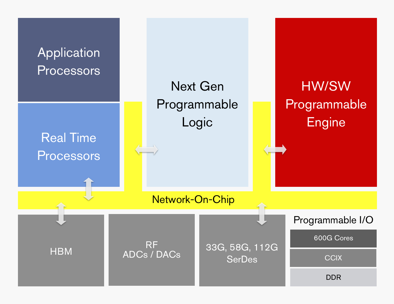
The ACAP architecture will include both application and real-time processors as well as programmable logic for digital signal processing (DSP) and a hierarchy of distributed memory. The chip will also feature a high-speed network-on-a-chip linking the functional blocks and arbitrating between them.
ACAP will support various generations of DDR memory and certain family devices will include high-bandwidth 3D stacked memory. There will also be device members that use RF analogue-to-digital and digital-to-analogue converters.
In turn, ACAP will have fast input-output circuitry with serial/deserialisers (SERDES) running at 33, 58 and even 112 gigabit-per-second (Gbps) rates. Xilinx demonstrated its latest 112Gbps serdes at the recent OFC show held in San Diego.
Certain ACAP devices will use a novel engine that is software and hardware programmable. Programming the engine at the software level will require some embedded expertise.
“We are always looking at how we can use our hardware programming expertise to get another level of optimisation beyond just software-programmable blocks,” says Peng. Xilinx will detail the engine’s workings later this year.
Xilinx says the 7nm ACAP will deliver a 20x AI compute performance improvement and 4x the 5G communications bandwidth compared to its current 16nm FPGAs.
The company has already delivered software tools for ACAP to select customers and expects first device shipments in 2019.
Data-centre focus
Peng, who has been CEO since January, says the data centre market is now Xilinx’s top priority segment.
Data centres require ever more computing while their networked architectures continue to evolve. This represents an attractive market for Xilinx especially given its programmable devices not only serve computing but also storage and networking requirements.
Xilinx has also been expanding its software development environments that let its devices be programmed at a higher level by developers that have little or no knowledge of the underlying hardware. This contrasts with traditional Xilinx FPGA users that by nature are hardware engineers. “There are easily 1000x more software developers than FPGA developers,” says Peng.
Companies such as Amazon, Alibaba, Huawei, Baidu, Nimbix and Tencent also offer FPGAs-as-a-service as part of their cloud offerings.
The central role of software in data centres may have caused chips to recede into the background, yet Xilinx will argue that the nature of the silicon has never been more important.
Infinera’s ICE flow
Infinera’s newest Infinite Capacity Engine 5 (ICE5) doubles capacity to 2.4 terabits. The ICE, which comprises a coherent DSP and a photonic integrated circuit (PIC), is being demonstrated this week at the OFC show being held in San Diego.
Infinera has also detailed its ICE6, being developed in tandem with the ICE5. The two designs represent a fork in Infinera’s coherent engine roadmap in terms of the end markets they will address.
 Geoff BennettThe ICE5 is targeted at data centre interconnect and applications where fibre in being added towards the network edge. The next-generation access network of cable operators is one such example. Another is mobile operators deploying fibre in preparation for 5G.
First platforms using the ICE5 will be unveiled later this year and will ship early next year.
Infinera’s ICE6 is set to appear two years after the ICE5. Like the ICE4, Infinera’s current Infinite Capacity Engine, the ICE6 will be used across all of Infinera’s product portfolio.
Meanwhile, the 1.2 terabit ICE4 will now be extended to work in the L-band of optical wavelengths alongside the existing C-band, effectively doubling a fibre’s capacity available for service providers.
Infinera’s decision to develop two generations of coherent designs follows the delay in bringing the ICE4 to market.
“The fundamental truth about the industry today is that coherent algorithms are really hard,” says Geoff Bennett, director, solutions and technology at Infinera.
By designing two generations in parallel, Infinera seeks to speed up the introduction of its coherent engines. “With ICE5 and ICE6, we have learnt our lesson,” says Bennett. “We recognise that there is an increased cadence demanded by certain parts of the industry, predominately the internet content providers.”
ICE5
The ICE5 uses a four-wavelength indium-phosphide PIC that, combined with the FlexCoherent DSP, supports a maximum symbol rate of 66Gbaud and a modulation rate of up to 64-ary quadrature amplitude modulation (64-QAM).
Infinera says that the FlexCoherent DSP used for ICE5 is a co-development but is not naming its partners.
Using 64-QAM and 66Gbaud enables 600-gigabit wavelengths for a total PIC capacity of 2.4 terabits. Each PIC is also ‘sliceable’, allowing each of the four wavelengths to be sent to a different location.
Infinera is not detailing the ICE5’s rates but says the design will support lower rates, as low as 200 gigabit-per-second (Gbps) or possibly 100Gbps per wavelength.
Bennett highlights 400Gbps as one speed of market interest. Infinera believes its ICE5 design will deliver 400 gigabits over 1,300km. The 600Gbps wavelength implemented using 64-QAM and 66Gbaud will have a relatively short reach of 200-250km.
“A six hundred gigabit wavelength is going to be very short haul but is ideal for data centre interconnect,” says Bennett, who points out that the extended reach of 400-gigabit wavelengths is attractive and will align with the market emergence of 400 Gigabit Ethernet client signals.
Probabilistic shaping squeezes the last bits of capacity-reach out of the spectrum
Hybrid Modulation
The 400-gigabit will be implemented using a hybrid modulation scheme. While Infinera is not detailing the particular scheme, Bennett cites several ways hybrid modulation can be implemented.
One hybrid modulation technique is to use a different modulation scheme on each of the two light polarisations as a way of offsetting non-linearities. The two modulation schemes can be repeatedly switched between the two polarisation arms. “It turns out that the non-linear penalty takes time to build up,” says Bennett.
Another approach is using blocks of symbols, varying the modulation used for each block. “The coherent receiver has to know how many symbols you are going to send with 64-QAM and how many with 32-QAM, for example,” he says
A third hybrid modulation approach is to use sub-carriers. In a traditional coherent system, a carrier is the output of the transmit laser. To generate sub-carriers, the coherent DSP’s digital-to-analogue converter (DAC) applies a signal to the modulator which causes the carrier to split into multiple sub-carriers.
To transmit at 32Gbaud, four sub-carriers can be used, each modulated at 8Gbaud, says Bennett. Nyquist shaping is used to pack the sub-carriers to ensure there is no spectral efficiency penalty.
“You now have four parallel streams and you can deal with them independently,” says Bennett, who points out that 8Gbaud turns out to be an optimal rate in terms of minimising non-linearities made up of cross-phase and self-phase modulation components.
Sub-carriers can be described as a hybrid modulation approach in that each sub-carrier can be operated at a different baud rate and use a different modulation scheme. This is how probabilistic constellation shaping - a technique that improves spectral efficiency and which allows the data rate used on a carrier to be fine-tuned - will be used with the ICE6, says Infinera.
For the ICE5, sub-carriers are not included. “For the applications we will be using ICE5 for, the sub-carrier technology is not as important,” says Bennett. “Where it is really important is in areas such as sub-sea.”
Silicon photonics has a lower carrier mobility. It is going to be harder and harder to build such parts of the optics in silicon.
Probabilistic constellation shaping
Infinera is not detailing the longer-term ICE6 beyond highlights two papers that were presented at the ECOC show last September that involved a working 100Gbaud sub-carrier-driven wavelength and probabilistic shaping applied to a 1024-QAM signal.
The 100Gbaud rate will enable higher capacity transponders while the use of probabilistic shaping will enable greater spectral efficiency. “Probabilistic shaping squeezes the last bits of capacity-reach out of the spectrum,” says Bennett.
“In ICE6 we will be doing different modulation on each sub-carrier,” says Bennett. “That will be part of probabilistic constellation shaping.” And assuming Infinera adheres to 8Gbaud sub-carriers, 16 will be used for a 100Gbaud symbol rate.
Infinera argues that the interface between the optics and the DSP becomes key at such high baud rates and it argues that its ability to develop both components will give it a system design advantage.
The company also argues that its use of indium phosphide for its PICs will be a crucial advantage at such high baud rates when compared to silicon photonics-based solutions. “Silicon photonics has a lower carrier mobility,” says Bennett. “It is going to be harder and harder to build such parts of the optics in silicon.”
ICE4 embraces the L-band
Infinera’s 1.2 terabit six-wavelength ICE4 was the first design to use Nyquist sub-carriers and SD-FEC gain sharing, part of what Infinera calls its advanced coherent toolkit.
At OFC, Infinera announced that the ICE4 will add the L-band in addition to the C-band. It also announced that the ICE4 has now been adopted across Infinera’s platform portfolio.
The first platforms to use the ICE4 were the Cloud Xpress 2, the compact modular platform used for data centre interconnect, and the XT-3300, a 1 rack-unit (1RU) modular platform targeted at long-haul applications.
A variant of the platform tailored for submarine applications, the XTS-3300, achieved a submarine reach of 10,500km in a trial last year. The modulation format used was 8-QAM coupled with SD-FEC gain-sharing and Nyquist sub-carriers. The resulting spectral efficiency achieved was 4.5bits/s/Hz. In comparison, standard 100-gigabit coherent transmission has a spectral efficiency of 2bits/s/Hz. The total capacity supported in the trial was 18.2 terabits.
Since then, the ICE4 has been added the various DTN-X chassis including the XT-3600 2.4 terabit 4RU platform.
Rockley Photonics showcases its in-packaged design at OFC
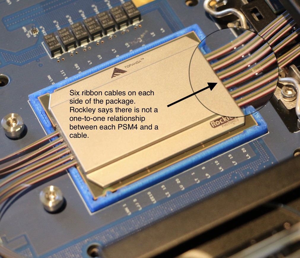
The packaged design includes Rockley's own 2 billion transistor layer 3 router chip, and its silicon photonics-based optical transceivers. The layer 3 router chip, described as a terabit device, also includes mixed-signal circuits needed for the optical transceevers' transmit and receive paths.
 Source: Rockley Photonics (annotated by Gazettabyte).
Rockley says it is using 500m-reach PSM4 transceivers for the design and that while a dozen ribbon cables are shown, this does not mean there are 12 100-gigabit PSM4 transceivers. The company is not saying what the total optical input-output is.
 Source: Rockley Photonics (annotated by Gazettabyte).
The company has said it is not looking to enter the marketplace as a switch chip player competing with the likes of Broadcom, Intel, Cavium, Barefoot Networks and Innovium. To develop such a device and remain competitive requires considerable investment and that is not Rockley's focus. Instead, it is using its router chip as a demonstrator to show the marketplace what can be done and that the technology works.
When asked what progress Rockley is making showcasing its technology, its CEO Andrew Rickman said: “It is going very well but nothing we can say publicly."
The switch chip makers continue to use electrical interfaces for their state-of-the-art switches which have a capacity of 12.8 terabits. It still remains to be seen which generation of switch chip will finally adopt in-packaged optics and whether on-board optics designs such as COBO will be adopted first.
For the full interview with CEO Andrew Rickman, click here.
DustPhotonics reveals its optical transceiver play
A start-up that has been active for a year has dropped its state of secrecy to reveal it is already shipping its first optical transceiver product.
The company, DustPhotonics, is backed by private investors and recently received an undisclosed round of funding that will secure the company’s future for the next two years.
Product plans
DustPhotonics' first product is the multi-mode 100m-reach 100GBASE-SR4 QSFP28. The company will launch its first 400-gigabit optical modules later this year.
 Ben Rubovitch
“We probably are going to be one of the first to market with [400-gigabit] QSFP-DD and OSFP multi-mode solutions,” says Ben Rubovitch, CEO of DustPhotonics.
The start-up has developed 50 gigabit-per-lane technology required for higher-speed modules such as the QSFP56, QSFP-DD and OSPF pluggables. The QSFP-DD form factor is designed to be backwards compatible with the QSFP and QSFP28 and is backed by the likes of Facebook and Cisco, while the OSFP is a new form factor supported by Google and switch maker Arista Networks.
DustPhotonics chose the 4-lane 25-gigabit QSFP28 to prove the working of its 50 gigabit-per-lane technology. “The reason we did that is that the PAM-4 chipsets weren’t ready when we started,” says Rubovitch. “So we invested the first year solving the production issues and the optical interface and used the QSFP28 as the platform.”
The challenge with a 50 gigabit-per-lane optical interface is that the photo-detector aperture used is smaller. “So on our QSFP28 we used a small photo-detector to prove the optical solution,” says Rubovitch.
The start-up is now developing faster speed multi-mode designs: a 200-gigabit QSFP56 pluggable, a 400-gigabit QSFP-DD implementing the 400GBASE-SR8 standard and a similar active optical cable variant; products that it hopes to sample in the second quarter of this year. This will be followed by similar SR8 implementations using the OSFP.
 DustPhotonics' optical product roadmap. Source: Gazettabyte/ DustPhotonics.
DustPhotonics is also adapting its optical packaging technology to support single-mode designs: the 500m IEEE 400GBASE-DR4 and the 2km 400G-FR4, part of the 100G Lambda multi-source agreement (MSA). Both the DR4 and FR4 designs use 100-gigabit optical lanes.
Technology
Rubovitch says that despite the many optical transceiver players and the large volumes of modules now manufactured, pluggable optics remain expensive. “The front panel of a top-of-rack switch [populated with modules] costs ten times more than the switch itself,” he says.
DustPhotonics has tackled the issue of cost by simplifying the module’s bill of materials and the overall manufacturing process.
The start-up buys the lasers and electronic ICs needed and adds its own free-space optics for both multi-mode and single-mode transceiver designs. “It is all plastic-molded so we don’t use any glass types or any integrated lasers and that simplifies much of the process,” says Rubovitch. Indeed, he claims the design reduces the bill of materials of its transceivers by between 30 and 50 percent.
The front panel of a top-of-rack switch [populated with modules] costs ten times more than the switch itself
DustPhotonics has also developed a passive alignment process. “We have narrowed the one accurate step - where we align the optics - to one machine,” says Rubovitch. “This compares to two steps ‘accurate’ and one step ‘align’ for active alignment.” Active alignment for a QSFP28 module takes ten minutes, he says, whereas DustPhotonics’ passive alignment process takes under a minute per module.
“There is also a previous manufacturing stage where we place the VCSELs and photo-detectors on a substrate itself and we don’t need accuracy here, unlike other solutions,” he says.
The overall result is a simpler, more cost-effective design. “We are already manufacturing in a volume production line and we see the numbers and how competitive we are, and it is going to create an even larger advantage at 400 gigabits,” says Rubovitch.
DustPhotonics’ passive alignment process takes under a minute per module
What next?
DustPhotonics is also developing embedded optics, where the optics are placed next to an ASIC, and even in-package designs where the optics and ICs are co-packaged.
Rubovitch says such technologies will be needed because of the very high power 100-gigabit electrical transceivers consume on a switch chip, for example, as well the silicon area they require; precious silicon real estate needed to cope with the ever-increasing packet-processing demands. “Bringing the optics very close [to the chip] can help solve those issues for the switch providers,” he says.
As Rockley Photonics’ CEO, Andrew Rickman, observed recently, combining optics with the switch silicon has long been discussed yet has still to be embraced by the switch chip makers. This explains why Rockley developed its own switch ASIC to demonstrate a complete in-packaged reference design.
Rubovitch agrees that the concept of optics replacing electrical interfaces has long been spoken of but that hasn’t happened due to copper speeds continuing to advance. There is already a 100 gigabit-per-lane solution that will meet the demands of the next generation of switch designs, he says: “It really depends on what is going to be the next leap: 200 gigabits or 400-gigabits.”
Using optics to replace electrical interfaces could come with the advent of 25 terabit switch silicon or maybe the generation after. “Or maybe something in between: 25 terabit solutions will start to move gradually to a more packaged solution or at least closer on-board optics,” concludes Rubovitch.
Lumentum jolts the industry with Oclaro acquisition
Lumentum announced on Monday its plan to acquire Oclaro in a deal worth $1.8 billion.
The prospect of consolidation among optical component players has long been mooted yet the announcement provided the first big news jolt at the OFC show, being held in San Diego this week.
 Alan Lowe“Combined, we will be an industry leader in telecom transmission and transport as well as 3D sensing,” said Alan Lowe, president and CEO of Lumentum, on an analyst call discussing the deal.
Lumentum says their joint revenues totalled $1.7 billion with a 39% gross margin over the last year. And $60 million in synergies are forecast in the second year after the deal closes, which is expected to happen later this year.
The $1.8 billion acquisition will comprise 56 percent cash and 44 percent Lumentum stock. Lumentum will also raise $550 million to help finance the deal.
“This is a big deal as it consolidates the telecom part of the component market,” says Daryl Inniss, business development manager at OFS Fitel and former market research analyst.
Background
Lowe said that ever since Lumentum became a standalone company three years ago, the firm concentrated on addressing the increase in optical communications demand that started in late 2015 and then last year on ramping the production of its 3D sensing components. “Execution on major M&As had to wait,” he said.
The company investigated potential acquisitions and evaluated several key technologies including silicon photonics and indium phosphide. This led to it alighting on Oclaro with its indium phosphide and photonic integrated circuit (PIC) expertise.
Lowe also highlighted Oclaro’s strategy of the last five years of first trimming its business lines and then successfully executing on delivering optical transmission products.
Oclaro’s CEO, Greg Dougherty, CEO of Oclaro, described how his company has focussed on delivering differentiated photonic chip products to various growing end markets. “This is a very good combination for both companies and for the industry,” said Dougherty.
There is no overabundance in [optical] chip designers worldwide and together we have the strongest chip designer team in the world
Business plans
Lumentum’s business includes telecom transport components, modules and sub-systems. Its products include reconfigurable optical add/drop multiplexers (ROADMs), pump lasers, optical amplifiers and submarine products. In the second half of 2017, Lumentum’s telecom revenue mix was split three quarters telecom transport with transmission products accounted for the remaining quarter. Other Lumentum businesses include industrial lasers and 3D sensing.
In contrast, Oclaro’s focus in solely transmission components and modules, with the revenue mix in its most recent quarter being 53 percent telecom line side and 47 percent datacom client-side products.
The combined R&D resources of the merged company will allow it to do a much better job at supporting datacom products using the new QSFP-DD and OSFP form factors. “Right now I’m guessing that Alan is spread thin and I know the Oclaro datacom team has been spread thin,” says Dougherty.
The acquisition will also pool the two companies’ fabrication facilities.
Lumentum has already moved its lithium niobate manufacturing to its main gallium arsenide and indium phosphide fab in San Jose, California. San Jose also hosts a separate planar lightwave circuit fab.
Oclaro, which is headquartered in San Jose, has three photonic chip fabrication sites: an indium phosphide laser fab for datacom in Japan that makes directly modulated lasers (DMLs) and electro-absorption modulated lasers (EMLs), an indium phosphide fab in the UK that manufactures coherent optical components and sub-assemblies, and a lithium niobate fab in Italy.
The acquisition will also bolster the company’s chip design resources. “There is no overabundance in [optical] chip designers worldwide and together we have the strongest chip designer team in the world,” says Dougherty.
Lumentum plans to assign some of the chip designers to tackle a burgeoning pipeline of 3D sensing product designs.
In 2017 Lumentum reported three customers that accounted for nearly half of its revenues, while Oclaro had four customers, each accounted for 10 percent or more of its sales, in 4Q 2017. Oclaro selected customers include the webscale players, Amazon, Google and Microsoft, as well as leading systems vendors such as Ciena, Cisco, Coriant, Huawei, Juniper, Nokia and ZTE.
Both Oclaro and Lumentum, along with Neophotonics, signed an agreement with Ciena a year ago to use its WaveLogic Ai DSP in their coherent module designs.
Lumentum plans to provide more deal details closer to its closure. Meanwhile, the two CEOs will continue to run their companies with Oclaro’s Dougherty remaining at least during the transition period.
Further information:
For the link to the acquisition presentation, click here.
Coherent gets a boost with probabilistic shaping
Nokia has detailed its next-generation PSE-3 digital signal processor (DSP) family for coherent optical transmission.
The PSE-3s is the industry’s first announced coherent DSP that supports probabilistic constellation shaping, claims Nokia.
Probabilistic shaping is the latest in a series of techniques adopted to improve coherent optical transmission performance. These techniques include higher-order modulation, soft-decision forward error correction (SD-FEC), multi-dimensional coding, Nyquist filtering and higher baud rates.
 Kyle Hollasch
“There is an element here that the last big gains have now been had,” says Kyle Hollasch, director of product marketing for optical networks at Nokia.
Probabilistic shaping is a signal-processing technique that squeezes the last bit of capacity out of a fibre’s spectrum, approaching what is known as the non-linear Shannon Limit.
“We are not saying we absolutely hit the Shannon Limit but we are extremely close: tenths of a decibel whereas most modern systems are a couple of decibels away from the theoretical maximum,” says Hollasch.
Satisfying requirements
Optical transport equipment vendors are continually challenged to meet the requirements of the telcos and the webscale players.
One issue is meeting the continual growth in IP traffic: telcos are experiencing 25 percent yearly traffic growth whereas for the webscale players it is 60 percent. Vendors must also ensure that their equipment keeps reducing the cost of transport when measured as the cost-per-bit.
Operators also want to automate their networks. Technologies such as flexible-grid, reconfigurable optical add/drop multiplexers (ROADMs), higher-order modulation and higher baud rates all add flexibility to the optical layer but at the expense of complexity.
There is an element here that the last big gains have now been had
“It is easy to say software-defined networking will hide all that complexity,” says Hollasch. “But hardware has an important role: to keep delivering capacity gains but also make the network simpler.”
Satisfying these demands is what Nokia set out to achieve when designing the PSE-3s.
Capacity and cost
Like the current PSE-2 coherent DSPs that Nokia launched in 2016, two chips make up the PSE-3 family: the super coherent PSE-3s and the low-power compact PSE-3c.
The PSE-3s is a 1.2-terabit chip that can drive two sets of optics, each capable of transmitting 100 to 600 gigabit wavelengths. This compares to the 500-gigabit PSE-2s that can drive two wavelengths, each up to 250Gbps.
The low-power PSE-3c also can transmit more traffic, 100 and 200-gigabit wavelengths, twice the capacity of the 100-gigabit PSE-2c.
Nokia has used a software model of two operators’ networks, one an North America and another in Germany, to assess the PSE-3s.
The PSE-3s’ probabilistic shaping delivers 70% more capacity while using a third fewer line cards when compared with existing commercial systems based on 100Gbps for long haul and 200Gbps for the metro. When the PSE-3s is compared with existing Nokia PSE-2s-based platforms on the same networks, a 25 percent capacity gain is achieved using a quarter fewer line cards.
Hollasch says that the capacity gain is 1.7x and not greater because 100-gigabit coherent technology used for long haul is already spectrally efficient. “But it is less so for shorter distances and you do get more capacity gains in the metro,” says Hollasch.
Probabilistic shaping
The 16nm CMOS PSE-3s supports a symbol rate of up to 67Gbaud. This compares to the 28nm CMOS PSE-2s that uses two symbol rates: 33Gbaud and 45Gbaud.
The PSE-3s’ higher baud rate results in a dense wavelength-division multiplexing (DWDM) channel width of 75GHz. Traditional fixed-grid channels are 50GHz wide. With 75GHz-wide channels, 64 lightpaths can fit within the C-band.
The PSE-3s uses one modulation format only: probabilistic shaping 64-ary quadrature amplitude modulation (PS-64QAM). This compares with the PSE-2s that supports six modulations ranging from binary phase-shift keying (BPSK) for the longest spans to 64-QAM for a 400-gigabit wavelength.
Using probabilistic shaping, one modulation format supports data rates from 200 to 600Gbps. For 100Gbps, the PSE-3s uses a lower baud rate in order to fit existing 50GHz-wide channels.
In current optical networks, all the constellation points of the various modulation formats are used with equal probability. BPSK has two constellation points while 64-QAM has 64. Probabilistic shaping does not give equal weighting to all the constellation points. Instead, it favours those with lower energy, represented by those points closer to the origin in a constellation graph. The only time all the constellation points are used is at the maximum data rate - 600Gbps for the PSE-3s.
Using the inner, lower energy constellation points more frequently than the outer points reduces the overall average energy and this improves the signal-to-noise ratio. That is because the symbol error rate at the receiver is dominated by the distance between neighbouring points on the constellation. Reducing the average energy still keeps the distance between the points the same, but since a constant signal power level is used for DWDM transmission, applying gain increases the distance between the constellation points.
“We separate these points further in space - the Euclidean distance between them,” says Hollasch. “That is where the shaping gain comes from.”
Changing the probabilistic shaping in response to feedback from the chip, from the network, we think that is a powerful innovation
Using probabilistic shaping delivers a maximum 1.53dB of improvement in a linear transmission channel. In practice, Nokia says it achieves 1dB. “One dB does not sound a lot but I call it the ultimate dB, the last dB in addition to all the other techniques,” he says.
By using few and fewer of the constellation points, or favouring those points closer to the origin, reduces the data that can be transported. This is how the data rate is reduced from the maximum 600Gbps to 200Gbps.
To implement probabilistic shaping, Nokia has developed an IP block for the chip called the distribution matcher. The matcher maps the input data stream as rates as high as 1.2 terabits-per-second onto the constellation points in a non-uniform way.
Theoretically, probabilistic shaping allows any chosen data rate to be used. But what dictates the actual data rate gradations is the granularity of the client signals. The Optical Internetworking Forum’s Flex Ethernet (FlexE) standard defines 25-gigabit increments and that will be the size of the line-side data rate increments.
Embracing a single modulation format and a 75GHz channel results in network operation benefits, says Hollasch: “It stops you having to worry and manage a complicated spectrum across a broad network.” And it also offers the prospect of network optimisation. “Changing the probabilistic shaping in response to feedback from the chip, from the network, we think that is a powerful innovation,” says Hollasch.
 The reach performance of the PSE-3s using 62Gbaud and PS-64QAM. The reach performance of the PSE-2s is shown (where relevant) for comparison purposes.
Product plans
The first Nokia product to use the PSE-3 chips is the 1830 Photonic Service Interconnect-Modular, a 1 rack-unit compact modular platform favoured by the webscale players.
Nokia has designed two module-types or ‘sleds’ for the 1830 PSI-M pizza box. The first is a 400-gigabit sled that uses two sets of optics and two PSE-3c chips along with four 100-gigabit client-side interfaces. Four such 400-gigabit sleds fit within the platform to deliver a total of 1.6 terabits of line-side capacity.
In contrast, two double-width sleds fit within the platform using the PSE-3s. Each sled has one PSE-3 chip and two sets of optics, each capable of up to a 600-gigabit wavelength, and a dozen 100-gigabit interfaces. Here the line-side capacity is 2.4 terabits.
Nokia says the 400-gigabit sleds will be available in the first half of this year whereas the 1.2 terabit sleds will start shipping at the year-end or early 2019. The first samples of the PSE-3s are expected in the second half of 2018. Nokia will then migrate the PSE-3s to the rest of its optical transport platform portfolio.
So has coherent largely run its course?
“In terms of a major innovation in signal processing, probabilistic shaping is completing the coherent picture,” says Hollasch. There will be future coherent DSP chips based on more advanced process nodes than 16nm with symbol rates approaching 100GBaud. Higher data rates per wavelength will result but at the expense of a wider channel width. But once probabilistic shaping is deployed, further spectral efficiencies will be limited.