
China Mobile plots 400 Gigabit trials in 2017
China Mobile is preparing to trial 400-gigabit transmission in the backbone of its optical network in 2017. The planned trials were detailed during a keynote talk given by Jiajin Gao, deputy general manager at China Mobile Technology, at the OIDA Executive Forum, an OSA event hosted at OFC, held in Los Angeles last week.
The world's largest operator will trial two 400-gigabit variants: polarisation-multiplexed, quadrature phase-shift keying (PM-QPSK) and 16-ary quadrature amplitude modulation (PM-16QAM).
The 400-gigabit 16-QAM will achieve a total transmission capacity of 22 terabits and a reach of 1,500km using ultra-low-loss fibre and Raman amplification, while with Nyquist PM-QPSK, the capacity will be 13.6 terabits and a 2000km reach. China Mobile started to deploy 100 gigabits in its backbone in 2013. It expects to deploy 400 gigabits in its metro and provisional networks from 2018.
Gao also detailed the growth in the different parts of China Mobile's network. Packet transport networking ports grew by 200,000 in 2016 to 1.2 million. The operator also grew its fixed broadband market share, adding over 20 million GPON subscribers to reach 80 million in 2016 while its optical line terminals (OLTs) grew from 89,000 in 2015 to 113,000 in 2016. Indeed, China Mobile has now overtaken China Unicom as China's second largest fixed broadband provider. Meanwhile, the fibre in its metro networks grew from 1.26 million kilometres in 2015 to 1.41 million in 2016.
The Chinese operator is also planning to adopt a hybrid OTN-reconfigurable optical add-drop multiplexer (OTN-ROADM) architecture which it trialled in the second half of 2016, linking several cities. The operator currently uses electrical cross-connect switches which were first deployed in 2011.
The ROADM is a colourless, directionless and contentionless design that also supports a flexible grid, and the operator is interested in using the hybrid OTN-ROADM in its provisional backbone and metro networks. Using the OTN-ROADM architecture is expected to deliver a power savings of between 13% and 50%, says Gao.
XG-PON was also first deployed in 2016. China Mobile says 95% of its GPON optical network units deployed connect single families. The operator detailed an advanced home gateway that it has designed which six vendors are now developing. The home gateway features application programming interfaces to enable applications to be run on the platform.
For the XG-PON OLTs, China Mobile is using four vendors - Fiberhome, Huawei, ZTE and Nokia Shanghai Bell. The OLTs support 8 ports per card with three of the designs using an ASIC and one an FPGA. "Our conclusion is that 10-gigabit PON is mature for commercialisation," says Gao.
Gao also talked about China Mobile's NovoNet 2020, the vision for its network which was first outlined in a White Paper in 2015. NovaNet will be based on such cloud technologies as software-defined networking (SDN) and network function virtualisation (NFV) and is a hierarchical arrangement of Telecom Integrated Clouds (TICs) that span the core through to access. He outlined how for private cloud services, a data centre will have 3,000 servers typically while for public cloud 4,000 servers per node will be used.
China Mobile has said the first applications on NovoNet will be for residential services, with LTE, 5G enhanced packet core and multi-access edge computing also added to the TICs.
The operator said that it will trial SDN and NFV in its network this year and also mentioned how it had developed its own main SDN controller that oversees the network.
China Mobile reported 854 million mobile subscribers at the end of February, of which 559 million are LTE users, while its wireline broadband users now exceed 83 million.
Reflections on OFC 2017
Mood, technologies, notable announcements - just what are the metrics to judge the OFC 2017 show held in Los Angeles last week?
It was the first show I had attended in several years and the most obvious changes were how natural the presence of the internet content providers now is alongside the telecom operators, as well as systems vendors exhibiting at the show. Chip companies, while also present, were fewer than before.
 Source: OSA
Another impression were the latest buzz terms: 5G, the Internet of Things and virtual reality-augmented reality. Certain of these technologies are more concrete than others, but their repeated mention suggests a consensus that the topics are real enough to impact optical components and networking.
It could be argued that OFC 2017 was the year when 400 Gigabit Ethernet became a reality
The importance of 5G needs no explanation while the more diffuse IoT is expected to drive networking with the huge amounts of data it will generate. But what are people seeing about virtual reality-augmented reality that merits inclusion alongside 5G and IoT?
Another change is the spread of data rates. No longer does one rate represent the theme of an OFC such as 40 Gigabits or 100 Gigabits. It could be argued that OFC 2017 was the year when 400 Gigabit Ethernet became a reality but there is now a mix of relevant rates such as 25, 50, 200 and 600 gigabits.
Highlights
There were several highlights at the show. One was listening to Jiajin Gao, deputy general manager at China Mobile Technology, open the OIDA Executive Forum event by discussing the changes taking place in the operator's network. Gao started by outlining the history of China Mobile's network before detailing the huge growth in ports at different points in the network over the last two years. He then outlined China Mobile's ambitious rollout of new technologies this year and next.
China's main three operators have 4G and FTTx subscriber numbers that dwarf the rest of the world. Will 2017 eventually be seen as the year when the Chinese operators first became leaders in telecom networking and technologies?
The Executive Forum concluded with an interesting fireside discussion about whether the current optical market growth is sustainable. The consensus among representatives from Huawei, Hisense, Oclaro and Macom was that it is; that the market is more varied and stable this time compared to the boom and bust of 1999-2001. As Macom’s Preetinder Virk put it: "The future has nothing to do with the past". Meanwhile, Huawei’s Jeffrey Gao still expects strong demand in China for 100 gigabits in 2017 even if growth is less strong than in 2016. He also expects the second quarter this year to pick up compared to a relatively weak first quarter.
OFC 2017 also made the news with an announcement that signals industry change: Ciena's decision to share its WaveLogic Ai coherent DSP technology with optical module vendors Lumentum, Oclaro and NeoPhotonics.
The announcement can be viewed several ways. One is that the initiative is a response to the success of Acacia as a supplier of coherent modules and coherent DSP technology. System vendors designed their own coherent DSP-ASICs to differentiate their optical networking gear. This still holds true but the deal reflects how the progress of merchant line-side optics from the likes of Acacia is progressing and squeezing the scope for differentiation.
The deal is also a smart strategic move by Ciena which, through its optical module partners, will address new markets and generate revenues as its partners start to sell modules using the WaveLogic Ai. The deal also has a first-mover advantage. Other systems vendors may now decide to offer their coherent DSPs to the marketplace but Ciena has partnerships with three leading optical module makers and is working with them on future DSP developments for pluggable modules.
The deal also raises wider questions as to the role of differentiated hardware and whether it is subtly changing in the era of network function virtualisation, or whether it is a reflection of the way companies are now collaborating with each other in open hardware developments like the Telecom Infra Project and the Open ROADM MSA.
Another prominent issue at the show is the debate as to whether there is room for 200 Gigabit Ethernet modules or whether the industry is best served by going straight from 100 to 400 Gigabit Ethernet.
Facebook and Microsoft say they will go straight to 400 gigabits. Cisco agrees, arguing that developing an interim 200 Gigabit Ethernet interface does not justify the investment. In contrast, Finisar argues that 200 Gigabit Ethernet has a compelling cost-per-bit performance and that it will supply customers that want it. Google supported 200 gigabits at last year’s OFC.
Silicon photonics
Silicon photonics was one topic of interest at the show and in particular how the technology continues to evolve. Based on the evidence at OFC, silicon photonics continues to progress but there were no significant developments since our book (co-written with Daryl Inniss) on silicon photonics was published late last year.
One of the pleasures of OFC is being briefed by key companies in rapid succession. Intel demonstrated at its booth its silicon photonics products including its CWDM4 module which will be generally available by mid-year. Intel also demonstrated a 10km 4WDM module. The 4WDM MSA, created last year, is developing a 10km reach variant based on the CWDM4, as well as 20km and 40km based designs.
Meanwhile, Ranovus announced its 200-gigabit CFP2 module based on its quantum dot laser and silicon photonics ring resonator technologies with a reach approaching 100km. The 200 gigabit is achieved using 28Gbaud optics and PAM-4.
Elenion Technologies made several announcements including the availability of its monolithically integrated coherent modulator receiver after detailing it was already supplying a 200 gigabit CFP2-ACO to Coriant. The company was also demonstrating on-board optics and, working with Cavium, announced a reference architecture to link network interface cards and switching ICs in the data centre.
I visited Elenion Technologies in a hotel suite adjacent to the conference centre. One of the rooms had enough test equipment and boards to resemble a lab; a lab with a breathtaking view of the hills around Los Angeles. As I arrived, one company was leaving and as I left another well-known company was arriving. Elenion was using the suite to demonstrate its technologies with meetings continuing long after the exhibition hall had closed.
Two other silicon photonics start-ups at the show were Ayar Labs and Rockley Photonics.
Ayar Labs in developing a silicon photonics chip based on a "zero touch" CMOS process that will sit right next to complex ASICs and interface to network interface cards. The first chip will support 3.2 terabits of capacity. The advantage of the CMOS-based silicon photonics design is the ability to operate at high temperatures.
Ayar Labs is using the technology to address the high-bandwidth, low-latency needs of the high-performance computing market, with the company expecting the technology to eventually be adopted in large-scale data centres.
Rockley Photonics shared more details as to what it is doing as well as its business model but it is still to unveil its first products.
The company has developed silicon photonics technology that will co-package optics alongside ASIC chips. The result will be packaged devices with fibre-based input-output offering terabit data rates.
Rockley also talked about licensing the technology for a range of applications involving complex ICs including coherent designs, not just for switching architectures in the data centre that it has discussed up till now. Rockley says its first product will be sampling in the coming months.
Looking ahead
On the plane back from OFC I was reading The Undoing Project by Michael Lewis about the psychologists Danny Kahneman and Amos Tversky and their insights into human thinking.
The book describes the tendency of people to take observed facts, neglecting the many facts that are missed or could not be seen, and make them fit a confident-sounding story. Or, as the late Amos Tversky put it: "All too often, we find ourselves unable to predict what will happen; yet after the fact, we explain what did happen with a great deal of confidence. This 'ability' to explain that which we cannot predict, even in the absence of any additional information, represents an important, though subtle, flaw in our reasoning."
So, what to expect at OFC 2018? More of the same and perhaps a bombshell or two. Or to put it another way, greater unpredictability based on the impression at OFC 2017 of an industry experiencing an increasing pace of change.
IoT will drive chip design and new styles of computing
Looking back 20 years hence, how will this period be viewed? The question was posed by the CEO of imec, Luc Van de hove, during his opening talk at a day event imec organised in Tel-Aviv.
For Van den hove, this period will be seen as one of turbulent technological change. “The world is changing at an incredible rate,” he says. “The era of digital disruption is changing our industry and this disruption is not going to stop.”
 Luc Van den hove
It was the Belgium nonoelectronics R&D centre’s second visit to Israel to promote its chip and systems expertise as it seeks to expand its links with Israel’s high-tech industry. And what most excites imec is the Internet of Things (IoT), the advent of connected smart devices that turn data into information and adapt the environment to our needs.
The world is changing at an incredible rate. The era of digital disruption is changing our industry and this disruption is not going to stop
Internet of Things
Imec is focussing on five IoT areas: Smart Health - wearable and diagnostic devices, Smart Mobility which includes technologies for autonomous cars, drones and robots, Smart Cities, Smart Industry and Smart Energy. “In all these areas we look at how we can leverage our semiconductor know-how,” says Van den hove. “How we can bring innovative solutions by using our microchip technology.”
The broad nature of the IoT means imec must form partnerships across industries while strengthening its systems expertise. In healthcare, for example, imec is working with John Hopkins University, while last October, imec completed the acquisition of iMinds, a Belgium research centre specialising in systems software and security.
“One of the challenges of IoT is that there is not one big killer application,” says Van den hove. “How to bring these technologies to market is a challenge.” And this is where start-ups can play a role and explains why imec is visiting Israel, to build its partnerships with local high-tech firms.
Imec also wants to bring its own technologies to market through start-ups and has established a €100 million investment fund to incubate new ideas and spin-offs.
Technologies
Imec’s expertise ranges from fundamental semiconductor research to complex systems-on-chip. It is focussing on advanced sensor designs for IoT as this is where it feels it can bring an advantage. Imec detailed a radar chip design for cars that operates at 79GHz yet is implemented in CMOS. It is also developing a Light Detection and Ranging (LIDAR) chip for cars based on integrated photonics. Future cars will have between 50 to 100 sensors including cameras, LIDAR, radar and ultrasound.
 Imec's multi-project wafers. Source: imec
The data generated from these sensors must be processed, fused and acted upon. Imec is doing work in the areas of artificial intelligence and machine learning. In particular, it is developing neuromorphic computing devices that use analogue circuits to mimic the biological circuitry of the brain. Quantum computing is another area imec has begun to explore.
One of the challenges of IoT is that there is not one big killer application
“There is going to be so much data generated,” says Van den Hove. “And it is better to do it [processing] locally because computation is cheaper than bandwidth.”
Imec envisages a network with layers of intelligence, from the sensors all the way to the cloud core. As much of the data as possible will be processed by the sensor so that it can pass on more intelligent information to the network edge, also known as fog computing. Meanwhile, the cloud will be used for long-term data storage, for historical trending and for prediction using neuromorphic algorithms, says Van den Hove.
But to perform intensive processing on-chip and send the results off-chip in a power-efficient manner will require advances in semiconductor technology and the continuation of Moore’s law.
Moore's law
Imec remains confident that Moore’s law will continue to advance for some years yet but notes it is getting harder. In the past, semiconductor technology had a predictable roadmap such that chip designers could plan ahead and know their design goals would be met. Now chip technologists and designers must work together, a process dubbed technology-design co-optimisation.
Van den hove cites the example of imec’s work with ARM Holdings to develop a 7nm CMOS process node. “You can create some circuit density improvement just by optimising the design, but you need some specific technology features to do that,” he says. For example, by using a self-alignment technique, fewer metal tracks can be used when designing a chip's standard cell circuitry. "Using the same pitch you get an enormous shrink," he says. But even that is not going to be enough and techniques such as system-technology co-optimisation will be needed.
Imec is working on FinFETs, a style of transistor, to extend CMOS processes down to 5nm and then sees the use of silicon nanowire technology - first horizontal and then vertical designs - to extend the roadmap to 3nm, 2.5nm and even 1.8nm feature sizes.
Imec is also working on 3D chip stacking techniques that will enable multi-layer circuits to be built. “You can use specific technologies for the SRAM, processing cores and the input-output.” Imec is an active silicon photonics player, seeing the technology playing an important role for optical interconnect.
Imec awarded Gordon Moore a lifetime of innovation award last year, and Van den hove spent an afternoon at Moore’s home in Hawaii. Van den hove was struck with Moore’s humility and sharpness: “He was still so interested in the technology and how things were going.”
Stitching together disaggregated chips
The Optical Internetworking Forum (OIF) has begun work on a 112-gigabit electrical interface to connect chips in a multi-chip module.
The ultra-short-reach electrical interface for multi-chip modules adds to the OIF's ongoing CEI-112G project, started in August 2016, to develop a 112 gigabit-per-second (Gbps) serial electrical interface for next-generation optical modules.
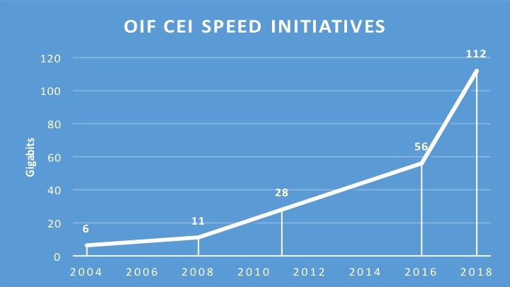 Source: Gazettabyte, OIF data. The year 2018 is an estimate.
The OIF is an industry organisation whose members include telcos, data centre operators, equipment makers and component companies. The OIF undertakes projects that range from high-speed interfaces, optical modules and flexible Ethernet through to programmable interfaces for Transport SDN. Each OIF project culminates in a published Implementation Agreement.
According to David Stauffer, of Kandou Bus and the OIF’s Physical and Link Layer Working Group Chair, the 112G multi-chip module initiative builds on earlier OIF work on a 56-gigabit ultra-short-reach (USR) interface that first addressed die-to-die communication. "We realised that there seems to be more than one application," says Stauffer. "The 112G project is expanded for these applications such that we will possibly end up with different solutions rather than just one."
Multi-chip modules
It was during the 56G USR work that the OIF first heard from members about the challenges of designing a system-on-chip and the idea of taking functions off-chip. High-capacity Ethernet switch chips, for example, are becoming so complex that future designs will not be able to support the long-reach serialisers-deserialisers (SerDes) circuits used for input-output due to the resulting design exceeding the chip's power constraints. “They [chip makers] were starting to think about offloading functions such as SerDes from the system-on-chip,” says Stauffer.
State-of-the-art chip designs can also include functions that occupying significant die area. “To better optimise chip and system costs, people are starting to think about the concept of breaking up the system-on-chip into multiple chips that are better optimised for cost and yield,” says Stauffer. He cites as an example a next-generation system-on-chip that interfaces to long-reach SerDes or optics, performs sensor processing and has significant on-board logic.
 David StaufferThe logic functions of such a chip are best implemented using an advanced 7nm CMOS process, yet SerDes design are not implemented in 7nm and won't be for some time yet. In turn, the sensor array may not even be implemented using a logic process. And if the logic circuitry occupies a significant die area, it may be more economical to split the logic into two chips, each of which will yield better. “Then I have a need for all these interfaces between these chips,” says Stauffer,
He stresses that the interfaces are split based on the the type of technology and on the size of the individual dies; the dies are not partitioned to minimise the bandwidth between them. This can result in significant bandwidth - terabits of capacity - between chips in the module. And to be cost-effective, the interfaces must be very low power.
Accordingly, interfaces between two logic chips or the logic function and the sensor array can require high bandwidth whereas interfaces to the SerDes may be a single lane and have different requirements in how it is clocked. “So there is some divergence in what may be the requirements,” says Stauffer. “The multi-chip module project allows for the fact that we may end up with two solutions.”
The OIF does not list companies involved in its projects. Kandou Bus is clearly one involved in the multi-chip module work, says Stauffer, and he points to similar work his company has done with Marvell but at lower rates. But a recent story in EETimes lists several companies.
Applications
Stauffer says there are several high-performance computing companies that are designing very high-end processing systems using new architectures. “They are going to use this stuff [multi-chip modules and 100G-plus interfaces] before it trickles down to the data centre,” he says.
For applications requiring sensor arrays, the sampling and control loops needed mean that in some cases the interface will need to support terabits-per-second of capacity, says Stauffer; the overall interface speed depending on the number of sensors in the array and the rate at which they sample.
The OIF ultra-short-reach interface is expected to work up to 116Gbps. Some members also want the interface to drive optical devices. “There is going to be a single lane interface at 100G-plus and others that consist of many parallel lanes,” says Stauffer.
The interface will operate over distances of 1cm to 2cm depending on the interposer technology used in the multi-chip module. Using an organic interposer will enable a reach of up to 2cm whereas a silicon interposer the distances will be 1cm or less.
A silicon interposer can be seen as a chip designed solely to interconnect the chips that sit on top, says Stauffer. The advantage of a silicon interposer is that it can supports thousands of input-outputs. But depending on its size and yield, the silicon interposer can be expensive. It also has higher-loss channels, explaining its shorter 1cm reach.
In contrast, an organic interposer is more in line with traditional multi-chip modules, says Stauffer. The interconnect density of an organic interposer is less than a silicon one due to the relatively large pad pitches it uses but the organic interposer is cheaper and has a lower insertion loss. “The OIF is designing something that is suitable for both,” says Stauffer.
No timetable has been given as to the duration of the multi-chip module interface work. But Stauffer says there are companies that would use the electrical interface now if it were available.
Presentation slides of the book
 A set of slides summarising the book, Silicon Photonics: Fueling the Next Information Revolution.
To download the slides, please click here.
The Open ROADM MSA adds new capabilities in Release 2.0
 Xavier PougnardThe Open ROADM MSA, set up by AT&T, Ciena, Fujitsu and Nokia, is promoting interoperability between vendors’ ROADMs by specifying open interfaces for their control using software-defined networking (SDN) technology. Now, one year on, the MSA has 10 members, equally split between operators and systems vendors.
Orange joined the Open ROADM MSA last July and says it shares AT&T’s view that optical networks lack openness given the proprietary features of the vendors’ systems.
“As service providers, we suffer from lock-in where our networks are composed of equipment from a single vendor,” says Xavier Pougnard, R&D manager for transport networks at Orange Labs. “When we want to introduce another vendor for innovation or economic reasons, it is nearly impossible.”
This is what the MSA group wants to tackle with its open specifications for the data and management planes. The goal is to enable an operator to swap equipment without having to change their control by using a common, open management interface. “Right now, for every new provider, we need IT development for the management of the [network] node,” says Pougnard.
As service providers, we suffer from lock-in where our networks are composed of equipment from a single vendor. When we want to introduce another vendor for innovation or economic reasons, it is nearly impossible.
MSA status
The Open ROADM MSA has published two data sets as part of its Release 1.2. One set tackles 100-gigabit data plane interoperability by defining what is needed for two line-side transponders to talk to each other. The second set of specifications uses the YANG modelling language to allow the management of the transponders and ROADMs.
The group is now working on Release 2.0 that will enable longer reaches and exploit OTN switching. The specifications will also support flexgrid whereas Release 1.2 specifies 50GHz fixed channels only. Release 2.0 is expected to be completed in the second quarter of 2017. “Service providers would like it as soon as possible,” says Pougnard.
Pougnard highlights the speed of development of an open MSA model with new releases issued every few months, far quicker that traditional standardisation bodies. It was this frustration with the slow pace of development of the standards bodies that led Orange to join the Open ROADM MSA.
Orange stresses that the Open ROADM will not be used for all dense wavelength-division multiplexing cases. There will be applications which require extended performance where a specific vendor's equipment will be used. “We do specify the use of an FEC [forward error correction] in the specification but there are more powerful FECs that extend the reach for 100-gigabit interfaces,” says Pougnard. But the underlying flexibility offered by the MSA trumps performance.
Trials
AT&T detailed in December a network demonstration of the Open ROADM technology. The operator used a 100-gigabit optical wavelength in its Dallas area network to connect two IP-MPLS routers using transponders and ROADMs from Ciena and Fujitsu.
Orange is targeting its own lab trials in the first half of this year using a simplified OpenDaylight SDN controller working with ROADMs from three systems vendors. “We want to showcase the technology and prove the added value of an open ROADM,” says Pougnard.
Orange is also a member of the Telecom Infra Project, a venture that includes Facebook and 10 operators to tackle telecom networks from access to the core. The two groups have had discussions about areas of possible collaboration but while the Open ROADM MSA wants to promote a single YANG model that includes the amplifiers of the line system, TIP expects there to be more than a single model. The two organisations also differ in their philosophies: the Open ROADM MSA concerns itself with the interfaces to the platforms whereas TIP also tackles the internal design of platforms.
Coriant, which is a member of TIP and the Open ROADM MSA, is keen for alignment. "As an industry we should try to make sure that certain elements such as open API definitions are aligned between TIP and the Open ROADM MSA," says Uwe Fischer, CTO of Coriant.
Meanwhile, the Open ROADM MSA will announce another vendor member soon and says additional operators are watching the MSA’s progress with interest.
Pougnard stresses how open developments such as the ROADM MSA require WDM engineers to tackle new things. “We have a tremendous shift in skills,” he says. “Now they need to work on the automation capability, on YANG modelling and Netconf.” Netconf - the IETF’s network configuration protocol - uses YANG models to enable the management of network devices such as ROADMs.
Acacia looks to co-package its coherent PIC and DSP-ASIC
- Acacia Communications is working to co-package its coherent DSP and its silicon photonics transceiver chip.
- The company is also developing a digital coherent optics module that will support 400 gigabit.
Acacia Communications is working to co-package its coherent DSP and its silicon photonics transceiver chip. The line-side optical transceiver company is working on a digital coherent optics module that will support 400 gigabits.
Acacia announced last November that it was sampling the industry’s first CFP2 Digital Coherent Optics (CFP2-DCO) that supports 100- and 200-gigabit line rates. The CFP2-DCO integrates the DSP and its silicon photonics chip within a CFP2 module, which is half the size of a CFP module, with each chip packaged separately.
The CFP2-DCO adds to the company’s CFP2-ACO design that was announced a year ago. In the CFP2-ACO, the CFP2 module contains just the optics with the DSP-ASIC chip on the same line card connected to the module via a special high-speed interface connector.
Now, Acacia is working to co-package the two chips, which will not only improve the performance of its CFP2-DCO but also enable new, higher-performance optical modules such as a 400-gigabit DCO. The Optical Internetworking Forum announced a new implementation agreement last December for an interoperable 400-gigabit ZR (80km) coherent interface.
Both [the DSP and silicon photonics chip] are based on CMOS processes. The next step for Acacia is to bring them into a single package.
Portfolio upgrades
Acacia has also upgraded its existing portfolio of coherent transceivers. The company has integrated the enhanced silicon photonics coherent transceiver in its AC100-CFP and its AC-400 5x7-inch modules.
The silicon-photonics transceiver achieves a more efficient coupling of light in and out of the chip and uses an improved modulator driver design that reduces the overall power consumption. The design also supports flexible grid, enabling channel sizes of 37.5GHz in addition to fixed-grid 50GHz channels.
The resulting AC100-CFP module has a greater reach of 2,500km and a lower power consumption than the first generation design announced in 2014. The enhanced PIC has also been integrated within the AC-400. The AC-400, announced in 2015, integrates two silicon photonics chips to support line rates of 200, 300 and 400 gigabits.
CFP2-DCO
Acacia is using the coherent transceiver photonic integrated circuit (PIC), first used in its CFP2-ACO, alongside a new coherent DSP to integrate the optics and DSP within the compact CFP2.
“The third-generation PIC is a mini PIC; in a gold box that is about the size of a dime, which is a third of the size of our original PIC,” says Benny Mikkelsen, founder and CTO of Acacia.
One design challenge with its latest DSP was retaining the reach of the original DSP used in the AC100-CFP while lowering its power consumption. Having an inherently low-power coherent DSP design in the first place is one important factor. Mikkelsen says this is achieved based on several factors such as the DSP algorithms chosen and how they are implemented in hardware, the clock frequencies used within the chip, how the internal busses are implemented, and the choice of bits-per-symbol used for the processing.
The resulting DSP’s power consumption can be further reduced by using an advanced CMOS process. Acacia uses a 16nm CMOS process for its latest DSP.
Other challenges to enable a CFP2-DCO module include reducing the power consumption of the optics and reducing the packaging size. “The modulator driver is the piece part that consumes the most power on the optics side,” says Mikkelsen.
Acacia's CFP2-DCO supports polarisation multiplexing, quadrature phase-shift keying (PM-QPSK) for 100 gigabits, and two modulation schemes: polarisation multiplexing, 8-ary quadrature amplitude multiplexing (PM-8QAM) and 16-ary QAM - for 200-gigabit line rates. In contrast, its -ACO supports just PM-QPSK and PM-16QAM.
At 100 gigabits, the DSP consumes about half the power of the Sky DSP used in the original AC100. Using PM-8QAM for 200 gigabits means the new DSP and optics support a higher baud rate - some 45 gigabaud compared to the traditional 32-35 gigabaud used for 100 and 200-gigabit transmission. However, while this increases the power consumption, the benefit of 8QAM is a 200-gigabit reach beyond 1,000km.
Mikkelsen stresses that a key reason the company can achieve a CFP2-DCO design is having both technologies in-house: “You can co-optimise the DSP and the silicon photonics”.
We think, at least in the near term, that the OSPF module seems to be a good form factor to work on
ACO versus DCO
Since Acacia now offers both the CFP2-ACO and CFP2-DCO modules, it is less concerned about how the relative demand for the two modules develops. “We don’t care too much which one is going to have the majority of the market,” says Mikkelsen. That said, Acacia believes that the CFP2-DCO market will become the larger of the two.
When the CFP2-ACO was first considered several years ago, the systems vendors and optical module makers shared a common interest. Systems vendors wanted to use their custom coherent DSP-ASICs while the -ACO module allowed component makers that didn't have the resources to develop their own DSP to address the market with their optics. It was also necessary to separate the DSP and the optics if the smaller CFP2 form factor was to be used.
But bringing CFP2-ACOs to volume production has proved more difficult than first envisaged. The CFP2-DCO is far easier to use, says Mikkelsen. The module can be plugged straight into equipment whereas the CFP2-ACO must be calibrated by a skilled optical engineer when a wavelength is first turned up.
Future work
Acacia is now looking at new module form factors and new packaging technologies. “Both [the DSP and silicon photonics chip] are based on CMOS processes,” says Mikkelsen. “The next step for Acacia is to bring them into a single package.”
In addition to the smaller size, a single package promises a slightly lower power consumption as well as manufacturing cost advantages. “We also expect to see higher performance once the DSP and optics are sitting next to each other which we believe will improve signal integrity between the two,” says Mikkelsen.
Acacia is not waiting for any industry challenges to be overcome for a single-package design to be achieved. The company points out that its silicon photonics chip is not temperature sensitive, aiding its co-packaging with the DSP.
Acacia is working on a 400-gigabit DCO design and is looking at several potential module types. The company is a member of the OSFP module MSA as well as the Consortium of On-Board Optics (COBO) which has started a coherent working group. “We think, at least in the near term, that the OSPF module seems to be a good form factor to work on,” says Mikkelsen.
Silicon Photonics Merging Ahead
"Silicon photonics has made considerable progress in a relatively short time to emerge as an important systems technology whose time has come"
FSAN unveils roadmap plans
Part 2: Next-generation passive optical networks
The Full Service Access Network (FSAN) has outlined its vision for fibre access networks for the coming decade.
FSAN is an industry forum that includes over 20 operators and 70 members overall. The group identifies service requirements and develops optical access technologies that are passed to the International Telecommunication Union (ITU) for standardisation.
 Source: FSAN
“One of the messages of the roadmap is that, in the immediate future, what FSAN wants to do is evolve the existing standards,” says Peter Dawes, FSAN NGPON co-chair.
The latest FSAN technologies to become standards are XGS-PON (10 gigabits symmetrical passive optical network) and the multiple wavelength TWDM-PON (time wavelength-division multiplexing passive optical network), also known as NG-PON2 (see chart).
PON status
XGS-PON is a single-wavelength PON standard that supports two rates: a 10-gigabit symmetrical rate and the asymmetrical 10 gigabits downstream (to the user) and 2.5 gigabits upstream originally introduced by XG-PON.
 Peter Dawes
TWDM-PON uses four wavelengths to deliver up to 40 gigabits of symmetrical bandwidth and has an option for eight wavelengths overall. TWDM-PON also uses tuneable lasers enabling operators to move subscribers between wavelengths.
“FSAN operators see continued growth in PON deployment,” says Dawes. “There is still strong deployment of GPON and we are on the verge of needing 10-gigabit symmetrical services.” Other operators may delay and go straight to TWDM-PON, he says.
According to Dawes, operators are seeing a variety of applications that are driving the need for 10-gigabit access rates. One is the growing use of video and video conferencing. Another bandwidth driver for access networks is mobile applications such as connecting mobile antennas and mobile backhaul. In addition, there are digital home trends such as social networking and the moving of content to the cloud.
Mobile fronthaul can eat as much bandwidth as you can supply once you start to aggregate [radio] antennas
Operators are also keen to attach the labels ‘gigabit’ and ‘gigabit services’ to their broadband offerings as a marketing differentiator.
Other drivers for the move to the newer PON technologies include peer-to-peer services and business IP services, says Dawes.
Roadmap
FSAN’s plan to evolve the existing standards in the near term will take the group to 2021.
One obvious way the existing PONs can be evolved is to adopt 25-gigabit wavelengths. This would enable a 25-gigabit symmetrical extension to XGS-PON and a future TWDM-PON variant with up to 200 gigabits of capacity if the full eight wavelengths are used. “It is a case of looking for logical evolutions of these technologies,” says Dawes.
One application that could use such high capacities is mobile fronthaul, says Dawes: “It can eat as much bandwidth as you can supply once you start to aggregate [radio] antennas.”
After 2020, FSAN will investigate disruptive technologies as it defines future optical access schemes. R&D work, new modulation schemes and component developments including silicon photonics will all be assessed as to their suitability for future optical access schemes.
Meanwhile, FSAN says it will review its roadmap on a yearly basis and amend it as required.
See Part 1: XGS and TWDM passive optical networks, click here
Telefonica tests XGS-PON
Part 1: XGS and TWDM passive optical networks
Telefonica is the latest operator to test XGS-PON, the 10-gigabit passive optical networking standard.
“Operators want to show they are taking the maximum from their fibre investment,” says Ana Pesovic, marketing manager for fibre at Nokia, the supplier of the XGS-PON equipment used for the operator’s lab tests. “Telefonica has been really aggressive in their fibre deployments in the last couple of years.”
 Ana Pesovic
XGS-PON
Approved by the ITU-T in 2016, XGS-PON supports two rates: 10-gigabit symmetrical and the asymmetrical rate of 10 gigabits downstream (to the user) and 2.5 gigabits upstream.
XGS-PON has largely superseded the earlier XG-PON standard which supports the 10-gigabit asymmetrical rate only. “It is fair to say there is no traction for XG-PON,” says Pesovic. “Even in China [an early adopter of XG-PON], we see the interest slowly moving to XGS-PON.”
Nokia says it has now been involved in 40 XGS-PON trials and nine customers have deployed the technology. “These have just started and they are not massive deployments,” says Pesovic.
Nokia’s XGS-PON customers include China Telecom and SK Broadband. SK Broadband has deployed XGS-PON alongside the more advanced TWDM-PON (time wavelength division multiplexing, passive optical network), the ITU-T NG-PON2 standard.
XGS-PON uses a fixed wavelength to deliver either the 10-gigabit symmetrical or asymmetrical service. The standard supports a distance of 20km and a split ratio of up to 1:128 - one XGS-PON optical line terminal (OLT) serving up to 128 optical network units (ONUs). In contrast, TWDM-PON supports four wavelengths enabling up to 40-gigabit symmetrical rates. And unlike XGS-PON, TWDM-PON supports flexible wavelengths using tuneable lasers.
The wavelengths used by XGS-PON and TWDM-PON have been specified such that the two standards can operate alongside GPON on the same fibre. Accordingly, with SK Broadband’s deployment, the two PON standards along with GPON support an aggregate capacity of 52.5 gigabits-per-second.
As well as testing XGS-PON's performance, Telefonica has tested that XGS-PON works without disturbing existing broadband services over its GPON networks, says Pesovic.
For the test, Telefonica used an 8-port line card where each port can be configured for XGS-PON or as a wavelength of a TWDM-PON. The line card fits within Nokia’s 7360 Intelligent Services Access Manager (ISAM) FX platform.
5G will require the deployment of many more small cells. With XGS-PON, multiple small cells can be served using a single PON
Applications
XGS-PON with its symmetrical 10-gigabit rate is suited to business services. "Operators can use one network to converge business and residential; today they are two overlay networks,” says Pesovic. Many businesses require 1-gigabit connectivity or less but by having a 10-gigabit link, multiple enterprises can be aggregated on one PON.
Nokia says that in countries such as South Korea as well as in Europe and North America there is also interest in a 10-gigabit PON for residential services. “People are taking the downstream bandwidth for granted and now the upstream is becoming a differentiator, making the quality of experience much better,” says Pesovic.
The bulk of traffic is still predominately downstream but increasingly users want to upload large files and video. Even if these uploads are of shorter duration, the network must deliver, says Pesovic.
Operators are also eyeing XGS-PON for the emerging 5G cellular standard. Nokia points out that 5G will require the deployment of many more small cells. With XGS-PON, multiple small cells can be served using a single PON.
Nokia expects XGS-PON will be deployed for years to come. Broadband is advancing by adding more wavelengths. To GPON, which uses one wavelength, can be added a second wavelength supporting 10-gigabit XGS-PON. Using TWDM-PON adds four and potentially eight more wavelengths - 40 gigabits and 80 gigabits of bandwidth, respectively. “It really doesn’t matter what the technology is called,” says Pesovic.
One North American operator is looking at TWDM-PON as a way to save power. During the night when there is less broadband usage, the operator wants to use wavelength mobility to migrate users onto a single wavelength.
TWDM-PON
Besides wavelength count, TWDM-PON differs from XGS-PON in its use of tuneable lasers.
Having tuneable wavelengths delivers several benefits to the operators. One is load balancing. If users on one wavelength start to exhaust its capacity, several users can be moved to a second wavelength that is less heavily loaded.
TWDM-PON also benefits network sharing and wavelength unbundling. A third-party operator can offer its fibre to interested operators. “Each operator could then operate on a single wavelength,” says Pesovic. If a user changes operator, they can simply be moved from one wavelength to another.
There are also operational benefits. If a fault develops on a board, users can be migrated to a second card without service interruption and the faulty board replaced.
One North American operator is looking at TWDM-PON as a way to save power, says Pesovic. During the night when there is less broadband usage, the operator wants to use wavelength mobility to migrate users onto a single wavelength. This would deliver sufficient bandwidth to those users that are active while allowing the remaining wavelengths to be powered down, saving power.
The issue impeding the uptake of TWDM-PON remains the high cost of tuneable lasers. Nokia expects it to be at least another year before the cost of tuneable lasers becomes more economical for PON. That said, service providers delivering businesses services may still be tempted to adopt TWDM-PON despite the higher cost of tuneable lasers given that the average revenue per user (ARPU) of business users is 5x that of residential users, says Pesovic.
See Part 2: FSAN unveils roadmap plans, click here