
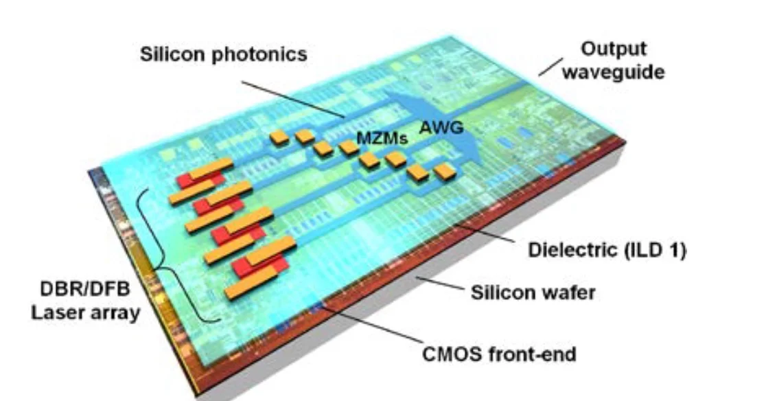
Elenion unveiled as a silicon photonics PIC company
- Elenion Technologies is making silicon photonics-based photonic integrated circuits
- The company has been active for two and a half years and has products already deployed
A privately-owned silicon photonics company that is already shipping products has dropped its state of secrecy to announce itself. Elenion Technologies is owned by Marlin Equity Partners, the investment firm that also owns systems vendor, Coriant.
“We are in the [optical] engine business,” says Larry Schwerin, CEO of Elenion Technologies. “We are developing a platform leveraging silicon photonics but we have other capabilities.”
 Larry SchwerinElenion’s expertise includes indium phosphide, radio frequency integrated circuits (RFICs), packaging, and driver and control electronics circuit design. The RFIC expertise suggests the company also plans to address the mobility market.
The company will detail its first products prior to the OFC show next March.
Telecom and Datacom
Elenion’s initial focus is the telecom market where its products are already deployed, with Coriant being a likely early customer. “We are also very active in datacom which has a different set of requirements,” says Schwerin.
Telecom is the harder 'trade space' of the two segments, says Schwerin. Telecom designs have to be outside-plant hardened and Telcordia-compliant. “Proving that world is a good place to get started and focussed,” he says.
In contrast, the datacom market has shorter equipment life cycles with optical designs deployed in a more controlled environment. Datacom customers also don't just want pluggables. “They want on-board solutions, parallel solutions, and they request a cost of $1-per-gigabit,” says Schwerin.
The company is targeting optical module makers, systems vendors and the cloud operators
The challenges facing the large-scale data centre operators are multifold: how they drive more bandwidth to the server, how they make the server more effective, how they scale their switching fabric, how they better use their fibre infrastructure and how they meet their optics cost targets.
Elenion says it has detailed data on the construction and costs of data centres and how they will scale. "You need to have that expertise in order to design the platform that they are trying to do today and going forward," says Schwerin. The company is working to deliver an optical engine that will help the data centre operators address the issues of distance, power consumption, space and signal integrity, and which will meet their $1-per-gigabit cost target.
We have developed a set of tools and a set of expertise that lets us design very complex integrated optoelectronic systems at the chip scale
Expertise
Elenion is limited in what it can say until its first products are unveiled. What is clear is that the silicon photonics company has a photonic integrated circuit (PIC) capability that it is using for on-board optics and for pluggable designs such as the CFP2.
 Michael Hochberg
“We have developed a set of tools and a set of expertise that lets us design very complex integrated opto-electronic systems at the chip scale,” says Michael Hochberg, CTO of Elenion.
According to Hochberg, Elenion is pulling complexity out of other systems and putting it into silicon. The value of such PICs is that it avoids having to deploy discrete optics such as lenses. And silicon is the ideal platform for scaling complexity, says Hochberg: “All the areas that we have developed expertise are things that we believe will need to be co-designed with the PIC.”
In the electronics industry, you tape things out and you expect them to work. That is what we are replicating here.
The company says it is building up a capability that has long existed in the semiconductor industry. "In the electronics industry, you tape things out and you expect them to work," says Hochberg. "That is what we are replicating here."
For datacom applications, Schwerin says that in addition to the PIC’s function, the company has developed a wafer-scale approach to packaging. Here, devices are packaged while still on the wafer rather than having to dice the wafer first. “You have got to get into the volumes of millions, not tens or hundreds of thousands,” says Schwerin. “That forces you into that space.”
The company is targeting optical module makers, systems vendors and the cloud operators as customers.
Origins
Schwerin was formerly the CEO of Capella Intelligent Subsystems, a developer of wavelength-selective switch technology, that was sold to Alcatel-Lucent (now Nokia) in 2013.
Hochberg was a director at the Optoelectronic Systems in Silicon (OpSIS) foundry and was a co-founder of silicon photonics company, Luxtera.
The two first met at a conference when Hochberg was running Silicon Lightwave Services (SLS), a silicon photonics design-for-service company. Schwerin became CEO of SLS and the company was bought by Merlin two and a half years ago to become Elenion. The name Elenion means starlight, a nod to J.R.R. Tolkien’s novels.
“We are now introducing ourselves as we are getting enough requests that it seemed the appropriate time,” says Schwerin.
TIP seeks to shake up the telecom marketplace
 Niall Robinson
Now, ten telcos, systems vendors, component and other players have joined Facebook as part of the Telecom Infra Project, or TIP, to bring the benefits of open-source design and white-box platforms to telecoms. TIP has over 300 members and has seven ongoing projects across three network segments of focus: access, backhaul, and core and management.
Facebook's involvement in a telecoms project is to benefit its business. The social media giant has 1.79 billion active monthly users and wants to make Internet access more broadly available. Facebook also has demanding networking requirements, both the linking of its data centres and supporting growing video traffic. It also wants better networks to support emerging services using technologies such as virtual reality headsets.
It is time to disrupt this closed market; it is time to reinvent everything we have today
The telecom operators want to collaborate with Facebook having seen how its Open Compute Project has created flexible, scalable equipment for the data centre. The operators also want to shake up the telecom industry. At the inaugural TIP summit held in November, the TIP chairman and CTO of SK Telecom, Alex Jinsung Choi, discussed how the scale and complexity of telecom networks make it hard for innovators and start-ups to enter the market. “It is time to disrupt this closed market; it is time to reinvent everything we have today,” said Choi during his TIP Summit talk.
Voyager
TIP unveiled a white-box packet optical platform dubbed Voyager at the summit. The one rack-unit (1RU) box is a project for backhaul. Voyager has been designed by Facebook and the platform’s specification has been made available to TIP.
Voyager is based on another platform Facebook has developed: the Wedge top-of-rack switch for the data centre. Wedge switches are now being made by several contract manufacturers. Each can be customised based on the operating system used and the applications loaded onboard. The goal is to adopt a similar approach with Voyager.
“Eventually, there will be something that is definitely market competitive in terms of hardware cost,” says Niall Robinson, vice president, global business development at ADVA Optical Networking, one of the companies involved in the Voyager initiative. “And you have got an open-source community developing a feature set from a software perspective.”
Other companies backing Voyager include Acacia Communications, Broadcom and Lumentum which are involved in the platform’s hardware design. Snaproute is delivering the software inside the box while first units are being made by the contract manufacturer, Celestica.
ADVA Optical Networking’s will provide a sales channel for Voyager and is interfacing it to its network management system. The system vendor will also provide services and software support. Coriant is another systems vendor backing the project. It is providing networking support including routeing and switching as well as dense WDM transmission capabilities.
This [initiative] has shown me that the whole supply and design chains for transport can be opened up; I find that fascinating.
Robinson describes TIP as one of the most ambitious and creative projects he has been involved in. “It is less around the design of the box," he says. "It is the shaking up of the ecosystem, that is what TIP is about.”
A 25-year involvement in transport has given Robinson an ingrained view that it is different to other aspects of telecom. For example, a vendor’s transport system must be at each end of the link due to the custom nature of platforms that are designed to squeeze maximum performance over a link. “In some cases, transport is different but what TIP maybe realises is that transport does not always have to be different,” says Robinson. “This [initiative] has shown me that the whole supply and design chains for transport can be opened up; I find that fascinating.”
Specification
At the core of the 1RU Voyager is the Broadcom StrataXGS Tomahawk. The 3.2-terabit switch chip is also the basis of the Wedge top-of-rack switch. The Tomahawk features 128 x 25 gigabit-per-second (Gbps) serdes to enable 32 x 100 gigabit ports, and supports layer-2 switching and layer-3 routeing.
Voyager uses 12, 100 Gigabit Ethernet client-side pluggable interfaces and four 200-gigabit networking interfaces based on Acacia’s AC-400 optical module. The AC-400 uses coherent optics and supports polarisation multiplexing, 16 quadrature amplitude modulation (PM-16QAM). “If it was a pure transport box the input rate would equal the output rate but because it is a packet box, you can take advantage of layer 2 over-subscription,” says Robinson.
At layer-3 the total routeing capacity is 2 terabits, the sum of the client and network interfaces. “At layer-3, the Tomahawk chip does not know what is a client port and what is a networking port; they are just Ethernet ports on that device,” says Robinson.
ADVA Optical Networking chose to back Voyager because it does not have a packet optical platform in its product portfolio. Until now, it has partnered with Juniper Networks and Arista Networks when such functionality has been needed. “We are chasing certain customers that are interested in Voyager,” says Robinson. “We are enabling ourselves to play in the packet optical space with a self-contained box.”
Status and roadmap
The Voyager is currently in beta-prototype status and has already been tested in trials. Equinix has tested the box working with Lumentum’s open line system over 140km of fiber, while operator MTN has also tested Voyager.
The platform is expected to be generally available in March or April 2017, by when ADVA Optical Networking will have completed the integration of Voyager with its network management system.
Robinson says there are two ways Voyager could develop.
 Source: Gazettabyte
One direction is to increase the interface and switching capacities of the 1RU box. Next-generation coherent digital signal processors that support higher baud rates will enable 400Gbps and even 600Gbps wavelengths using PM-64QAM. This could enable the line-side capacity to increase from the current 800Gbps to 2 or 3 terabits. And soon, 400Gbps client-side pluggable modules will become available. Equally, Broadcom is already sampling its next-generation Tomahawk II chip that has 6.4 terabits of switching capacity.
Another direction the platform could evolve is to add an backplane to connect multiple Voyagers. This is something already done with the Wedge '6-pack' that combines six Wedge switch cards. A Voyager 6-pack would result in a packet-optical platform with multiple terabits of switching and routeing capacity.
“This is an industry-driven initiative as opposed to a company-driven one,” says Robinson. “Voyager will go whichever way the industry thinks the lowest cost is.”
Corrected on Dec 22nd. The AC-400 is a 5"x7" module and not as originally stated.
NeoPhotonics samples its first CFP-DCO products
 The company has announced two such CFP Digital Coherent Optics (CFP-DCO) modules: a 100 gigabit-per-second (Gbps) module and a dual-rate 100Gbps and 200Gbps one.
“Our rationale [for entering the CFP-DCO market] is we have all the optical components and the [merchant coherent] DSPs are now becoming available,” says Ferris Lipscomb (pictured), vice president of marketing at NeoPhotonics. “It is possible to make this product without developing your own custom DSP, with all the expense that entails.”
-DCO versus -ACO
The pluggable transceiver line-side market is split between Digital Coherent Optics and Analog Coherent Optics (ACO) modules.
Optical module makers are already supplying the more compact CFP2 Analog Coherent Optics (CFP2-ACO) transceivers. The CFP2-ACO integrates the optics only, with the accompanying coherent DSP-ASIC chip residing on the line card. The CFP2-ACO suits system vendors that have their own custom DSP-ASICs and can offer differentiated, higher-transmission performance while choosing the optics in a compact pluggable module from several suppliers.
In contrast, the CFP-DCO suits more standard deployments, and for those end-customers that do not want to be locked into a single vendor and a proprietary DSP. The -DCO is also easier to deploy. In China, currently undertaking large-scale 100-gigabit optical transport deployments, operators want a module that can be deployed in the field by a relatively unskilled technician. Deploying an ACO requires an engineer to perform the calibration due to the analogue interface between the module and the DSP, says NeoPhotonics.
The DCO also suits those systems vendors that do not have their own DSP and do not want to source a merchant coherent DSP and implement the analogue integration on the line card.
Our rationale [for entering the CFP-DCO market] is we have all the optical components and the [merchant coherent] DSPs are now becoming available
One platform, two products
The two announced ClearLight CFP-DCO products are a 100 gigabit-per-second (Gbps) module implemented using polarisation multiplexing, quadrature phase-shift keying modulation (PM-QPSK), and a module that supports both 100Gbps and 200Gbps using PM-QPSK and 16 quadrature amplitude modulation (PM-16QAM), respectively.
The two modules share the same optics and DSP-ASIC. Where they differ is in the software loaded onto the DSP and the host interface used. The lower-speed module has a 4 by 25-gigabit interface whereas the 200-gigabit CFP-DCO uses an 8 by 25-gigabit-wide interface. “The 100-gigabit CFP-DCO plugs into existing client-side slots whereas the 200-gigabit CFPs have to plug into custom designed equipment slots,” says Lipscomb.
The 100-gigabit CFP-DCO has a reach of 1,000km plus and has a power consumption under 24W. Lipscomb points out that the actual specs including the power consumption are negotiated on a customer-by-customer basis. The 200-gigabit CFP-DCO has a reach of 500km.
NeoPhotonics says it is using a latest-generation 16nm CMOS merchant DSP. NTT Electronics (NEL) and Clariphy have both announced 16nm CMOS coherent DSPs.
“We are designing to be able to second-source the DSP,” says Lipscomb. “There are currently only two merchant suppliers but there are others that have developments but are not yet at the point where they would be in the market.”
The CFP-DCO modules also support flexible grid that can fit a carrier within the narrower 37.5GHz channel to increase overall transmission capacity sent across a fibre’s C-band.
NeoPhotonics’s 100Gbps CFP-DCO is already sampling and it expected to be generally available in mid-2017, while the 200Gbps CFP-DCO is expected to be available one-quarter later.
“For 200-gigabit, you need to have customers building slots,” says Lipscomb. “For 100-gigabit, there are lots of slots available that you can plug into; 200-gigabits will take a little bit longer.”
NeoPhotonics’ CFP-DCO delivers the line rate used by the Voyager white box packet optical switch being developed as part of the Telecom Infra Project backed by Facebook and ten operators including Deutsche Telekom and SK Telecom. But the one-rack-unit Voyager packet optical platform uses four 5"x7" modules not pluggable CFP-DCOs to achieve the total line rate of 800Gbps.
Roadmap
NeoPhotonics is developing coherent module designs that will use higher baud rates than the standard 32-35 gigabaud (Gbaud), such as 45Gbaud and 64Gbaud.
The company also plans to develop a CFP2-DCO. Such a module is expected around 2018 once lower-power DSP-ASICs become available that can fit within the 12W power envelope of the CFP2. Such merchant DSP-ASICs will likely be implemented in a more advanced CMOS process such as 12nm or even 7nm.
Acacia Communications is already sampling a CFP2-DCO. Acacia designs its own silicon photonics-based optics and the coherent DSP-ASIC.
NeoPhotonics is also considered future -ACO designs beyond the CFP2 such as the CFP8, the 400-gigabit OSFP form factor and even the CFP4. “We are studying it but we don't know yet which directions things are going to go,” says Lipscomb.
Corrected on Dec 22nd. The Voyager box does not use pluggable CFP-DCO modules.
Books of the year 2016 - Part 2
Simon Poole, director, new business ventures, Finisar Australia
The highlight of the year in fiction was reading The Shepherds’ Crown, the last of the Discworld novels from the wonderful Terry Pratchett. He, along with his cast of extraordinary characters, including the marvellous Tiffany Aching – a fabulous role model for teenage girls, held up a mirror to the foibles and strengths of our humanity, and will be sorely missed.
Farewell also to the fearless Christoph Hitchens; re-reading God is not Great reminded me of the strengths of his analysis and the importance of ethics and morals in our dealings with each other.
From a work perspective, The Other Side of Innovation: Solving the Execution Challenge by Vijay Govindarajan and Chris Trimble is one of the few books about innovation that tries to address the real issues which are, to my mind, around the implementation of the ideas rather than their generation. Recommended for anyone who has to manage innovation within an existing organisation with all its strengths and weaknesses.
Loudon Blair, senior director, corporate strategy office, Ciena
Three books read this year caused me to innocently stumble upon a recurring theme of how we are responding to rapid advances in communications technology.
As an adult, reading the 19th century classic, Alice’s Adventures in Wonderland by Lewis Carroll, provided a fascinating insight into Carroll’s creative mind. I was especially intrigued by how he plays with the reader’s interpretation of the English language - how we can say one thing and be understood to have said something else. It is a reminder in these days of email misinterpretation and text shorthand to be clear about what we intend to communicate.
The Alchemist by Paulo Coelho is a story of a shepherd boy seeking his personal legend and has multiple layers of interpretation. Coelho talks about how your personal legend is something that you have always wanted to accomplish. You know what it is when you are young because, at that age, everything is possible. But as you get older, you can lose track of your goal as some “mysterious force” convinces you that it is impossible to realize. However, Coelho says that when you really want something, “the universe conspires in helping you achieve it”.
I think there is a lot to be said for this idea that there is a universe of help out there to steer us towards our goals. As a society, we have never been more connected. Through the Internet and social networks, we have created a highly interactive and diverse networking universe which helps us attain our goals on a daily basis.
Drive: The Surprising Truth About What Motivates Us by Daniel H. Pink explores the issue of motivation in the workplace. Pink discusses how, as society evolves, traditional motivational techniques that may have been useful in the past, can be counter-productive in the future.
His discussion on how our workplace is evolving from routine rule-based tasks to non-routine conceptual tasks sidetracked me on to a commonly explored concern today about how artificial intelligence and robotics may replace many of today’s jobs.
As an engineer working to develop the next generation of the Internet, this caused me to reflect on the responsibility and implications of the future we will create as technical innovators.
Books of the year 2016 - Part 1
Each year Gazettabyte asks industry figures to comment on books that they recommend. Here are BT's Andrew Lord's and Cignal's Andrew Schmitt's recommendations to kick off this year's reviews.
Andrew Lord, Head of Optical Research at BT.
Quantum technologies are flavour of the month, with huge government investments from around the world. The title and cover of Bananaworld: Quantum Mechanics for Primates by Jeffrey Bub, suggest a book that will ‘unpeel’ a tough but increasingly important subject for general readers.
The book itself is, however, far deeper than its cover suggests, going way beyond the basics, and attempting to forge a link between quantum mechanics and the structure of information.
Imagining a strange world in which bananas exhibit quantum effects might just confuse rather than aid the general reader, but those wishing to probe the deeper information theory questions will find much here to ‘chew on’.
Andrew Schmitt, founder of Cignal AI
Starting a company with a wide customer base requires a lot of ‘infrastructure’ that I didn’t realise would consume so much time. I like to build things so it has been a real thrill but also a lot of work. I think I gravitated towards fun things to read as a result of having my hands full. All of them were outstanding.
A Fire Upon The Deep by Vernor Vinge, and Seveneves by Neal Stephenson require a great deal of mental fortitude but unfold on such a grand scale that they are very appealing. Stephenson is a favourite of mine, ever since reading Snow Crash in college. He’s like William Gibson except with a sense of humour.
I also reread Fahrenheit 451 by Ray Bradbury. Let’s just say it felt a lot less sci-fi the second time around. If you look at the monoculture of ideas in politics, education, even business – it’s a dangerous situation. A big reason populism is emerging in the West is because people are sick of getting told what to think by “smart” people, and the perceived loss of control. It is a healthy rebellion despite a lot of the downside because the alternative – everyone thinking in lockstep – is far more dangerous.
I had greater ambitions for non-fiction and have several unread Kindle books on my iPhone. I wanted to read The Hard Thing about Hard Things from Ben Horowitz but have not. Other titles include The Comeback: How Larry Ellison's Team Won the America's Cup by G. Bruce Knecht and American Sniper: The Autobiography of the Most Lethal Sniper in U.S. Military History by Chris Kyle.
The book Elon Musk: Tesla, SpaceX, and the Quest for a Fantastic Future by Ashlee Vance is a great read. There are a lot of haters out there who don’t like Tesla for various reasons – his government funding, climate-change skeptics who don’t like his views, and who knows what else? Fine by me. But after reading this book you have to acknowledge the massive, ridiculous undertaking of starting both a rocket company and an electric car company. It is insane. Yet this guy has managed to keep the wheels from coming off so far. He has burned through people, capital, and relationships but the results are impressive.
He may not be everyone's idea of a nice guy – whatever - but he is a walking, breathing, living image of the American ethos of invention and capitalism. Whatever money it costs the US government is more than offset by the example he sets for others that anything is possible provided you have enough time, money, and guts.
DIMENSION tackles silicon photonics’ laser shortfall
Several companies and research institutes, part of a European project, are developing a silicon photonics process that combines on-chip electronics and lasers. Dubbed Dimension (Directly Modulated Lasers on Silicon), the silicon photonics project is part of the European Commission’s Horizon 2020 research and innovation programme.
 The Dimension process showing the passive photonics, dielectric material, BiCMOS circuitry, and the on-chip lasers and modulators. The indium phosphide material is shown in red. Source: Dimension.
Goal
Silicon photonics has long been seen as a technology having the potential to deliver optical devices at CMOS manufacturing costs. But silicon's key shortfall is that it does not lase. “What we see with today’s solutions is a very low-cost chip with a lot of functionality, which is a great thing, but in addition you need lasers,” says Bert Offrein, principal research staff member and manager of neuromorphic devices and systems at IBM Research, a participant in the Dimension project.
The laser accounts for a relatively large fraction of the total bill of materials of a silicon photonics chip. In turn, connecting the light source to the chip is not trivial and adds to the packaging costs. “In this project, we try to tackle this [laser] issue,” says Offrein.
The project's goal is to develop manufacturing processes that will enable the integration of photonics, including the laser, and electronics, all on one chip. “By fully integrating the laser on the chip, we massively reduce the cost and create additional functionality,” says Offrein.
“This is the true embodiment of what people first pictured as silicon photonics: the combination of optics and electronics on a single chip,” says Lars Zimmermann, team leader, silicon photonics at the Innovations for High Performance Microelectronics (IHP) research institute, another member of Dimension.
Proof-of-concept demonstrators
Dimension is a four-year project that will end in early 2020. Other project participants besides IBM Research and the IHP include ADVA Optical Networking, Opticap and the Athens Information Technology (AIT) research centre. The Dresden University of Technology is overseeing the project.
The project has set itself the goal of producing three proof-of-concept designs using the integrated silicon photonics technology.
One is a 400 Gigabit Ethernet (GbE) transmitter made up of eight 50 gigabit-per-second (Gbps) channels, each comprising a 25 gigabaud directly-modulated laser combined with 4-level pulse amplitude modulation (PAM4). Two variants are planned: a directly modulated version for the 400GbE 2km reach specification, and one with external modulation for the 400GbE 10km reach standard.
Another design is a coherent transmitter for such applications as data centre interconnect, compromising a monolithically integrated narrow-linewidth tunable laser, modulator and driver. The coherent transmitter will have a 10km target reach, will operate at 25Gbps and have a tunable narrow linewidth of under 1MHz.
The third, final demonstrator is a directly-modulated 25-gigabit non-return-to-zero laser using indium phosphide grown directly on the silicon.
By fully integrating the laser on the chip, we massively reduce the cost and create additional functionality
Process details
The silicon photonics manufacturing process involves using a silicon-on-insulator (SOI) wafer to implement the passive photonics functions and the electronics. The electronics supports high-speed analogue driver transistors and a 0.25-micron BiCMOS process used to implement the chip's control logic and control interfaces.
 Bert Offrein
The laser is constructed by first bonding a thin layer of indium phosphide. “It is structured in such a way that it [the III-V material] can be embedded completely in the whole CMOS processing,” says Offrein.
The indium phosphide layer, referred to as a III-V membrane, sits on a thin dielectric layer placed on the SOI wafer. The dielectric material is needed to protect the wafer from contamination by the III-V material and ensure that such a design could be manufactured in a BiCMOS foundry.
Once the thin indium phosphide layer is deposited, the laser can be constructed. The final stages, part of the chip-making back-end process, is the adding of metallisation layers that connect the laser and the electronics, and the circuits to the interface signals.
Growing lasers on silicon
Growing the indium phosphide layer directly on silicon, as will be done for the third demonstrator, is more exploratory. “We want to show there is a path forward on this III-V-on-silicon technology to reduce the cost further,” says Offrein.
 Lars Zimmermann
The challenge growing indium phosphide on silicon is the lattice mismatch that occurs between the two materials which leads to defects.
To tackle the issue, an approach known as confined growth is used. A small ‘seed’ is put on the silicon to act as a growth point for the indium phosphide. A small cavity is created using silica to confine the resulting growth. “The material grows in this glass cavity and the defects grow out and disappear at the edges,” says Offrein. “You then have a very high-quality III-V in this glass and this is the starting point to continue to build the quantum wells that we need.”
One challenge is enlarging the confined growth area. So far, such growth is limited to a micron whereas the length of a laser can be 500 microns typically. And once the laser is built, there remain the issues of laser reliability and temperature stability. “We will see challenges but we are not there yet,” says Offrein.
This is the true embodiment of what people first pictured as silicon photonics: the combination of optics and electronics on a single chip
Status
Dimension is tackling designs for communications but such on-chip lasers will also be useful for a range of applications such as optical sensing, says Offrein.
The project is coming to the end of its first year. Its members are creating the basic building blocks needed to realise the lasers on the silicon wafer. IBM has demonstrated the basic functionality by bonding indium phosphide to its own passive silicon photonics technology. “We have also realised the first lasers - not yet electrically pumped but optically pumped,” says Offrein. The performance of these lasers is now being characterised.
All the processes needed to pump the lasers electrically are now in place and the goal is to build complete laser structures by March 2017.
IBM is also working with IHP to see what is required to implement the technology using IHP’s own silicon photonics process. IHP is currently testing IBM’s wafers regarding any contamination issues before testing the integration process.
ADVA Optical Networking would not be on board if they were not expecting eventually to have such technology available for their products
Exploitation
The European Commission has a long history of programmes backing leading-edge research. However, Europe's track record of exploiting such research to achieve market-leading companies and products has been limited.
The European Commission staff involved in planning the Horizon 2020 projects have been far more active in ensuring that these projects are exploited, says Zimmermann. "ADVA Optical Networking would not be on board if they were not expecting eventually to have such technology available for their products," he adds.
If Dimension proves successful, IHP could make available the integrated silicon photonics process to companies to implement their opto-electronic integrated circuit designs.
IBM, while no longer a semiconductor manufacturer, would also be keen for the technology to be transferred to large foundries such as STMicroelectronics and GlobalFoundries. “That way we could purchase the technology and apply it in our own systems,” says Offrein.
Article amended on Nov 29th. Added details about the proof-of-concept demonstrators.
Ciena brings data analytics to optical networking
- Ciena's WaveLogic Ai coherent DSP-ASIC makes real-time measurements, enabling operators to analyse and adapt their networks.
- The DSP-ASIC supports 100-gigabit to 400-gigabit wavelengths in 50-gigabit increments.
- The WaveLogic Ai will be used in Ciena’s systems from 2Q 2017.
Ciena has unveiled its latest generation coherent DSP-ASIC. The device, dubbed WaveLogic Ai, follows Ciena’s WaveLogic 3 family of coherent chips which was first announced in 2012. The Ai naming scheme reflects the company's belief that its latest chipset represents a significant advancement in coherent DSP-ASIC functionality.
 Helen XenosThe WaveLogic Ai is Ciena's first DSP-ASIC to support two baud rates, 35 gigabaud for fixed-grid optical networks and 56 gigabaud for flexible-grid ones. The design also uses advanced modulation schemes to optimise the data transmission over a given link.
Perhaps the most significant development, however, is the real-time network monitoring offered by the coherent DSP-ASIC. The data will allow operators to fine-tune transmissions to adapt to changing networking conditions.
“We do believe we are taking that first step towards a more automated network and even laying the foundation for the vision of a self-driving network,” says Helen Xenos, director, portfolio solutions marketing at Ciena.
All those assumptions of the past [based on static traffic] aren't holding true anymore
Network Analytics
Conservative margins are used when designing links due to a lack of accurate data regarding the optical network's status. This curtails the transmission capacity that can be sent since a relatively large link margin is used. In turn, cloud services and new applications mean networks are being exercised in increasingly dynamic ways. “The business environment has changed a little bit,” says Joe Cumello, vice president, portfolio marketing at Ciena. “All those assumptions of the past [based on static traffic] aren't holding true anymore.”
Ciena is being asked by more and more operators to provide information as to what is happening within their networks. Operators want real-time data that they can feed to analytics software to make network optimisation decisions. "Imagine a network where, instead of those rigid assumptions in place, run on manual spreadsheets, the network is making decisions on its own," says Cumello.
WaveLogic Ai performs real-time analysis, making available network measurements data every 10ms. The data can be fed through application programming interfaces to analytics software whose output is used by operators to adapt their networks.
 Joe Cumello
The network parameters collected include the transmitter and receiver optical power, polarisation channel and chromatic dispersion conditions, error rates and transmission latency. In addition, the DSP-ASIC separates the linear and non-linear noise components of the signal-to-noise ratio. An operator will thus see what the network margin is and allow links to operate more closely to the limit, improving transmissions by exploiting the WaveLogic Ai's 50-gigabit transmission increments.
"Maybe there are only a few wavelengths in the network such that the capacity can be cranked up to 300 gigabits. But as more and more wavelengths are added, if you have the tools, you can tell the operator to adjust,” says Xenos. “This helps them get to the next level; something that has not been available before.”
WaveLogic Ai
The WaveLogic Ai's lower baud rate - 35 gigabaud - is a common symbol rate used by optical transmission systems today. The baud rate is suited to existing fixed-grid networks based on 50GHz-wide channels. At 35 gigabaud, the WaveLogic Ai supports data rates from 100 to 250 gigabits-per-second (Gbps).
The second, higher 56 gigabaud rate enables 400Gbps single-wavelength transmissions and supports data rates of 100 to 400Gbps in increments of 50Gbps.
Using 35 gigabaud and polarisation multiplexing, 16-ary quadrature amplitude modulation (PM-16QAM), a 200-gigabit wavelength has a reach is 1,000km.
With 35-gigabaud and 16-QAM, effectively 8 bits per symbol are sent.
In contrast, 5 bits per symbol are used with the faster 56 gigabaud symbol rate. Here, a more complex modulation scheme is used based on multi-dimensional coding. Multi-dimensional formats add additional dimensions to the four commonly used based on real and imaginary signal components and the two polarisations of light. The higher dimension formats may use more than one time slot, or sub-carriers in the frequency domain, or even use both techniques.
For the WaveLogic Ai, the 200-gigabit wavelength at 56 gigabaud achieves a reach of 3,000km, a threefold improvement compared to using a 35 gigabaud symbol rate. The additional reach occurs because fewer constellation points are required at 56 gigabaud compared to 16-QAM at 35 gigabaud, resulting in a greater Euclidean distance between the constellation points. "That means there is a higher signal-to-noise ratio and you can go a farther distance," says Xenos. "The way of getting to these different types of constellations is using a higher complexity modulation and multi-dimensional coding."
We do believe we are taking that first step towards a more automated network and even laying the foundation for the vision of a self-driving network
The increasingly sophisticated schemes used at 56 gigabaud also marks a new development whereby Ciena no longer spells out the particular modulation scheme used for a given optical channel rate. At 56 gigabaud, the symbol rate varies between 4 and 10 bits per symbol, says Ciena.
The optical channel widths at 56 gigabaud are wider than the fixed grid 50GHz. "Any time you go over 35 gigabaud, you will not fit [a wavelength] in a 50GHz band," says Xenos.
The particular channel width at 56 gigabaud depends on whether a super-channel is being sent or a mesh architecture is used whereby channels of differing widths are added and dropped at network nodes. Since wavelengths making up a super-channel go to a single destination, the channels can be packed more closely, with each channel occupying 60GHz. For the mesh architecture, guard bands are required either side of the wavelength such that a 75GHz optical channel width is used.
The WaveLogic Ai enables submarine links of 14,000km at 100Gbps, 3,000km links at 200Gbps (as detailed), 1,000km at 300Gbps and 300km at 400Gbps.
Hardware details
The WaveLogic Ai is implemented using a 28nm semiconductor process known as fully-depleted silicon-on-insulator (FD-SOI). "This has much lower power than a 16nm or 18nm FinFET CMOS process," says Xenos. (See Fully-depleted SOI vs FinFET)

Using FD-SOI more than halves the power consumption compared to Ciena’s existing WaveLogic 3 coherent devices. "We did some network modelling using either the WaveLogic 3 Extreme or the WaveLogic 3 Nano, depending on what the network requirements were," says Xenos. "Overall, it [the WaveLogic Ai] was driving down [power consumption] more than 50 percent." The WaveLogic 3 Extreme is Ciena's current flagship coherent DSP-ASIC while the Nano is tailored for 100-gigabit metro rates.
Other Ai features include support for 400 Gigabit Ethernet and Flexible Ethernet formats. Flexible Ethernet is designed to support Ethernet MAC rates independent of the Ethernet physical layer rate being used. Flexible Ethernet will enable Ciena to match the client signals as required to fill up the variable line rates.
Further information:
SOI Industry Consortium, click here
STMicroelectronics White Paper on FD-SOI, click here
Other coherent DSP-ASIC announcements in 2016
Infinera's Infinite Capacity Engine, click here
Nokia's PSE-2, click here
Talking markets: Oclaro on 100 gigabits and beyond
Oclaro’s chief commercial officer, Adam Carter, discusses the 100-gigabit market, optical module trends, silicon photonics, and why this is a good time to be an optical component maker.
Oclaro has started its first quarter 2017 fiscal results as it ended fiscal year 2016 with another record quarter. The company reported revenues of $136 million in the quarter ending in September, 8 percent sequential growth and the company's fifth consecutive quarter of 7 percent or greater revenue growth.
 Adam CarterA large part of Oclaro’s growth was due to strong demand for 100 gigabits across the company’s optical module and component portfolio.
The company has been supplying 100-gigabit client-side optics using the CFP, CFP2 and CFP4 pluggable form factors for a while. “What we saw in June was the first real production ramp of our CFP2-ACO [coherent] module,” says Adam Carter, chief commercial officer at Oclaro. “We have transferred all that manufacturing over to Asia now.”
The CFP2-ACO is being used predominantly for data centre interconnect applications. But Oclaro has also seen first orders from system vendors that are supplying US communications service provider Verizon for its metro buildout.
The company is also seeing strong demand for components from China. “The China market for 100 gigabits has really grown in the last year and we expect it to be pretty stable going forward,” says Carter. LightCounting Market Research in its latest optical market forecast report highlights the importance of China’s 100-gigabit market. China’s massive deployments of FTTx and wireless front haul optics fuelled growth in 2011 to 2015, says LightCounting, but this year it is demand for 100-gigabit dense wavelength-division multiplexing and 100 Gigabit Ethernet optics that is increasing China’s share of the global market.
The China market for 100 gigabits has really grown in the last year and we expect it to be pretty stable going forward
QSFP28 modules
Oclaro is also providing 100-gigabit QSFP28 pluggables for the data centre, in particular, the 100-gigabit PSM4 parallel single-mode module and the 100-gigabit CWDM4 based on wavelength-division multiplexing technology.
2016 was expected to be the year these 100-gigabit optical modules for the data centre would take off. “It has not contributed a huge amount to date but it will start kicking in now,” says Carter. “We always signalled that it would pick up around June.”
One reason why it has taken time for the market for the 100-gigabit QSFP28 modules to take off is the investment needed to ramp manufacturing capacity to meet the demand. “The sheer volume of these modules that will be needed for one of these new big data centres is vast,” says Carter. “Everyone uses similar [manufacturing] equipment and goes to the same suppliers, so bringing in extra capacity has long lead times as well.”
Once a large-scale data centre is fully equipped and powered, it generates instant profit for an Internet content provider. “This is very rapid adoption; the instant monetisation of capital expenditure,” says Carter. “This is a very different scenario from where we were five to ten years ago with the telecom service providers."
Data centre servers and their increasing interface speed to leaf switches are what will drive module rates beyond 100 gigabits, says Carter. Ten Gigabit Ethernet links will be followed by 25 and 50 Gigabit Ethernet. “The lifecycle you have seen at the lower speeds [1 Gigabit and 10 Gigabit] is definitely being shrunk,” says Carter.
Such new speeds will spur 400-gigabit links between the data centre's leaf and spine switches, and between the spine switches. “Two hundred Gigabit Ethernet may be an intermediate step but I’m not sure if that is going to be a big volume or a niche for first movers,” says Carter.
400 gigabit CFP8
Oclaro showed a prototype 400-gigabit module in a CFP8 module at the recent ECOC show in September. The demonstrator is an 8-by-50 gigabit design using 25 gigabaud optics and PAM-4 modulation. The module implements the 400Gbase-LR8 10km standard using eight 1310nm distributed feedback lasers, each with an integrated electro-absorption modulator. The design also uses two 4-wide photo-detector arrays.
“We are using the four lasers we use for the CWDM4 100-gigabit design and we can show we have the other four [wavelength] lasers as well,” says Carter.
Carter says IP core routers will be the main application for the 400Gbase-LR8 module. The company is not yet saying when the 400-gigabit CFP8 module will be generally available.
We can definitely see the CFP2-ACO could support 400 gigabits and above
Coherent
Oclaro is already working with equipment customers to increase the line-side interface density on the front panel of their equipment.
The Optical Internetworking Forum (OIF) has already started work on the CFP8-ACO that will be able to support up to four wavelengths, each supporting up to 400 gigabits. But Carter says Oclaro is working with customers to see how the line-side capacity of the CFP2-ACO can be advanced. “We can definitely see the CFP2-ACO could support 400 gigabits and above,” says Carter. “We are working with customers as to what that looks like and what the schedule will be.”
And there are two other pluggable form factors smaller than the CFP2: the CFP4 and the QSFP28. “Will you get 400 gigabits in a QSFP28? Time will tell, although there is still more work to be done around the technology building blocks,” says Carter.
Vendors are seeking the highest aggregate front panel density, he says: “The higher aggregate bandwidth we are hearing about is 2 terabits but there is a need to potentially going to 3.2 and 4.8 terabits.”
Silicon photonics
Oclaro says it continues to watch closely silicon photonics and to question whether it is a technology that can be brought in-house. But issues remain. “This industry has always used different technologies and everything still needs light to work which means the basic III-V [compound semiconductor] lasers,” says Carter.
“Producing silicon photonics chips versus producing packaged products that meet various industry standards and specifications are still pretty challenging to do in high volume,” says Carter. And integration can be done using either silicon photonics or indium phosphide. “My feeling is that the technologies will co-exist,” says Carter.
COBO: specification work nearing completion
The Consortium for On-board Optics (COBO) is on target to complete its specifications work by the year end. The work will then enter a final approval stage that will take up to a further three months.

On-board optics, also known as mid-board or embedded optics, have been available for years but vendors have so far had to use custom products. The goal of COBO, first announced in March 2015 and backed by such companies as Microsoft, Cisco Systems, Finisar and Intel, is to develop a technology roadmap and common specifications for on-board optics to ensure interoperability.
Brad Booth (pictured), the chair of COBO and principal architect for Microsoft’s Azure Global Networking Services, says that bringing optics inside systems raises a different set of issues compared to pluggable optical modules used on the front panel of equipment. “If you have a requirement for 32 ports on a faceplate, you know mechanically what you can build,” says Booth.
With on-board optics, the focus is less about size considerations and more about the optical design itself and what is needed to make it work. There is also more scope to future-proof the design, something that can not be done so much with pluggable optics, says Booth.
COBO is working on a 400-gigabit optical module based on the 8-by–50 gigabit interface. The focus in recent months has been on defining the electrical connector that will be needed. The group has narrowed down the choice of candidates to two and the final selection will be based on the connector's signal integrity performance and manufacturability. Also being addressed is how two such modules could be placed side-by-side to create an 800-gigabit (16-by–50 gigabit) design.
COBO’s 400-gigabit on-board optics will support multi-mode and single-mode fibre variants. “When we do a comparison with what the pluggable people are pushing, there are a lot of pluggables that won’t be able to handle the power envelope,” says Booth.
There is no revolutionary change that goes on with technology, it all has to be evolutionary
On-board optics differs from a pluggable module in that the optics and electronics are not confined within a mechanical enclosure and therefore power dissipation is less of an design issue. But by supporting different fibre requirements and reaches new design issues arise. For example, when building a 16-by–50 gigabit design, the footprint is doubled and COBO is looking to eliminate the gap between the two such that a module can be plugged in that is either 8- or 16-lanes wide.
COBO is also being approached about supporting other requirements such as coherent optics for long-distance transmission. A Coherent Working Group has been formed and will meet for the first time in December in Santa Barbara, California. Using on-board optics for coherent avoids the power constraint issues associated with using a caged pluggable module.
On-board optics versus co-packaging
On-board optics is seen as the next step in the evolution of optics as it moves from the faceplate onto the board, closer to the ASIC. There is only so many modules that can fit on a faceplate. The power consumption also raises as the data rate of a pluggable modules increases, as does the power associated with driving faster electrical traces across the board.
Using on-board optics shortens the trace lengths by placing the optics closer to the chip. The board input-output capacity that can be supported also increases as it is fibres not pluggable optics that reside on the front panel. Ultimately, however, designers are already exploring the combining of optics and the chip using a system-in-package design, also known as 2.5D or 3D chip packaging.
Booth says discussions have already taken place between COBO members about co-packaged optics. But he does not expect system vendors to stay with pluggable optics and migrate directly to co-packaging thereby ignoring the on-board optics stage.
“There is no revolutionary change that goes on with technology, it all has to be evolutionary,” says Booth, who sees on-board optics as the next needed transition after pluggables. “You have to have some pathway to learn and discover, and figure out the pain points,” he says. “We are going to learn a lot when we start the deployment of COBO-based modules.”
Booth also sees on-board optics as the next step in terms of flexibility.
When pluggable modules were first introduced they were promoted as allowing switch vendors to support different fibre and copper interfaces on their platforms. The requirements of the cloud providers has changed that broad thinking, he says: “We don’t need that same level of flexibility but there is still a need for suporting different styles of optical interfaces on a switch.”
There are not a lot of other modules that can do 600 gigabit but guess what? COBO can
For example, one data centre operator may favour a parallel fibre solution based on the 100-gigabit PSM4 module while another may want a 100-gigabit wavelength-division multiplexing (WDM) solution and use the CWDM4 module. “This [parallel lane versus WDM] is something embedded optics can cater for,” says Booth.
Moving to a co-packaged design offers no such flexibility. What can a data centre manager do when deciding to change from parallel single-mode optics to wavelength-division multiplexing when the optics is already co-packaged with the chip? “Also how do I deal with an optics failure? Do I have to replace the whole switch silicon?” says Booth. We may be getting to the point where we can embed optics with silicon but what is needed is a lot more work, a lot more consideration and a lot more time, says Booth.
Status
COBO members are busy working on the 400-gigabit embedded module, and by extension the 800-gigabit design. There is also ongoing work as to how to support technologies such as the OIF’s FlexEthernet. Coherent designs will soon support rates such as 600-gigabit using a symbol rate of 64 gigabaud and advanced modulation. “There are not a lot of other modules that can do 600 gigabits but guess what? COBO can,” says Booth.
The good thing is that whether it is coherent, Ethernet or other technologies, all the members are sitting in the same room, says Booth: “It doesn’t matter which market gets there first, we are going to have to figure it out.”
Story updated on October 27th regarding the connector selection and the Coherent Working Group.
Telefónica tackles video growth with IP-MPLS network
- Telefónica’s video growth in one year has matched nine years of IP traffic growth
- Optical mesh network in Barcelona will use CDC-ROADMs and 200-gigabit coherent line cards
Telefónica has started testing an optical mesh network in Barcelona, adding to its existing optical mesh deployment across Madrid. Both mesh networks are based on 200-gigabit optical channels and high-degree reconfigurable add-drop multiplexers (ROADMs) that are part of the optical infrastructure that underpins the operator’s nationwide IP-MPLS network that is now under construction.
 Maria Antonia CrespoThe operator decided to become a video telco company in late 2014 to support video-on-demand and over-the-top streaming video services.
Telefónica realised its existing IP and aggregation networks would not be able to accommodate the video traffic growth and started developing its IP-MPLS network.
“What we are seeing is that the traffic is growing very quickly,” says Maria Antonia Crespo, IP and optical networking director at Telefónica. “In one year we are getting the same
figures as we got from internet traffic in the last nine years.”
The operator is rolling out the IP-MPLS network across Spain. Juniper Networks and Nokia are the suppliers of the IP router equipment, while Huawei and Nokia were chosen to supply the optical networking equipment.
IP-MPLS
Telefónica set about reducing the number of layers and number of hops when designing its IP-MPLS network. “At each hop, we have to invest money if we want to increase capacity,” says Crespo.

The result is an IP-MPLS network comprising four layers (see diagram). The uppermost Layer 1, dubbed HL1, connects the network to the internet world, while HL2 is a backbone transit layer. The HL3 layer is also a transit layer but at the provincial level. Spain is made up of 52 provinces. HL4 is where the services will reside, where Telefonica will deliver such services as Layer 2 and Layer 3 virtual private networks.
Between HL1 and HL2 is a national GMPLS-based photonic mesh, says Crespo, and between HL3 and HL4 there are the metro mesh networks. “Now we are deploying two GMPLS-based mesh networks, in Madrid and Barcelona,” she says. “Then, in the rest of the country, we are deploying [optical] rings.”
Systems requirements
Telefónica says it had several requirements when choosing the optical transport equipment, requirements common to both its backbone and regional networks.
One is the need to scale capacity at 10 gigabits and 100 gigabits, while network availability and robustness are also key. Telefónica says its network is designed to withstand two or more simultaneous fibre failures. “We have long experience with the GMPLS control plane to support different fibre impairments in the network,” says Alberto Colomer, optical technology manager at Telefónica.
The operator also wants its equipment to support high-speed interfaces and more granular rates to allow it to transition away from legacy traffic such as SDH and 1GbE. Operational improvements are another requirement: Telefónica wants to reduce the manual intervention its network needs. Optical time-domain reflectometers (OTDR) are being integrated into the network to monitor the fibre, as is the ability to automatically equalise the different optical channels.
 Alberto ColomerLastly, Telefónica is looking to reduce its capital expenditure and operational expense. It is deploying flexible rate 200-gigabit transponders in its Barcelona and Madrid networks and the same line cards will support 400-gigabit and even 1 terabit channels in future, as well as flexible grid to support the most efficient use of a fibre’s spectrum.
The 200-gigabit transponders use 16-quadrature amplitude modulation (16-QAM). Such transponders have enough reach to span each of the two cities but Colomer says Telefónica is still studying how many ROADM stages the 16-QAM transponders can cross.
It is like a pilot changing the engines while flying a plane
The ROADMs Telefónica is deploying in Madrid are directionless and are able to support up to 20 degrees. “You need some connectivity inside the mesh but also the mesh has to be connected to rings that cover all the counties around Madrid,” says Colomer.
Barcelona will be the first location where the ROADMs will also be colourless and contentionless (CDC-ROADMs). “We need to understand in a better way what are the advantages that come with that functionality,” says Colomer.
Telefónica has deployed Huawei’s Optix OSN 9800 platform in Madrid while in Barcelona Nokia’s 1830 Photonic Service Switch with the latest PSE-2 Coherent DSP-ASIC technology is being deployed.
Nokia’s PSS-1830 is designed to support the L-band as well as the C-band but Telefonica does not see the need for the L-band in the near future. “We are going in the direction of increasing capacity per channel: 400-gigabit channels and one terabit channels,” says Colomer. By deploying a photonic mesh and high-degree ROADMs, it will also be possible to increase capacity on a specific link by adding a fibre pair.
Status
The mesh in Madrid is already completed while Telefónica is deploying optical rings around Barcelona while it tests the contentionless ROADMs. These deployments are aligned with the IP-MPLS deployment, says Crespo, which is expected to be completed by 2018.
Crespo says the nationwide IP-MPLS rollout is a challenge. The deployment involves learning new technology that needs to be deployed alongside its existing network. "My boss likens it to a pilot changing the engines while flying a plane," says Crespo. "We are testing in the labs, duplicating it [the network], and migrating the traffic without impacting the customer."