
The making of integrated optics
A US initiative is bringing together leading companies with top academics and universities to create a manufacturing infrastructure for the widespread adoption of integrated photonics.
The US sees integrated photonics as a strategic technology and has set up the American Institute for Manufacturing Integrated Photonics - AIM Photonics - to advance the technology and make it available to a wider community of companies. AIM Photonics, with $610 million of public and private funding, is a five-year initiative ending in 2020. AIM’s long-term goal is to be self-sustaining.
 Doug Coolbaugh
“Right now the infrastructure is focussed on electronics and CMOS but photonics is going to be the future,” says Doug Coolbaugh, chief operations officer at AIM Photonics. “There is no other way to do it [very high bandwidth] except using light for ultra fast communications.”
Technologies start at universities and in the labs of companies with large R&D budgets. IBM and Intel, for example, have been developing silicon photonics for over a decade and the technology is ready for deployment. However, the intellectual property developed remains with such companies.
“AIM is not only creating the manufacturing infrastructure for integrated photonics but also ideas and intellectual property that can be used by companies for new products,” says Coolbaugh.
All the elements are being addressed so that small to medium businesses and entrepreneurial ventures can use integrated photonics for their products; companies too small to develop the technology themselves. “That will accelerate the silicon photonics ecosystem and allow new products to come out much faster than it would normally take,” says Coolbaugh.
Manufacturing
Silicon photonics luminary, Lionel Kimerling, professor of materials science and engineering at MIT, and an active member of AIM Photonics, views its focus on manufacturing as an important development.
The discipline of manufacturing is something that the chip industry has mastered through designing process integration, selecting materials and all the qualification standards used to meet system requirements, he says, but is less developed in the photonics industry.
AIM is making available a chip fabrication plant to interested companies. SUNY Polytechnic Institute has been working with MIT for the last six years to develop a 300mm-wafer silicon photonics line at its Albany site. The fab offers a multi-project wafer service whereby several designs can be made on a single wafer, allowing costs to be shared among companies.
AIM is not only creating the manufacturing infrastructure for integrated photonics but also ideas and intellectual property that can be used by companies for new products
A design kit is also being developed featuring key building blocks needed to make an integrated photonics circuit. AIM is working with leading semiconductor industry design automation companies Cadence, Synopsys and Mentor Graphics to provide the software tool environment for designers to develop circuits. “This design environment is compatible with the silicon photonics process here in our fab,” says Coolbaugh.
A packaging and prototyping facility located in Rochester, New York is also being set up. “Photonics packaging is relatively new and certain aspects have not been developed that much,” says Coolbaugh.
Another issue is developing skilled engineers and technicians able to design and manufacture integrated photonics circuits. Whereas electronic chip designers typically have a first degree, photonics engineers tend to have a doctorate because of the deep understanding needed. “This is one of the things we find we are lacking significantly,” says Coolbaugh. “There are just not enough skilled people in the industry to fulfil these needs.”
Professor Kimerling says he is spending much of his time putting together educational material to help attract individuals to pursue a career in silicon photonics. Much of the technology is in place, he says, what is required is to make it accessible to people. “I don’t have 40 more years in the industry, but I could influence the next 40 years by creating these instructional materials and career paths, and getting roadmap consensus that can drive the industry,” says Kimerling.
AIM is also working with universities and companies to develop technology and intellectual property alongside the manufacturing centres. Four research areas have been chosen, covering datacom, analogue RF for telecom involving Infinera, sensors and phased arrays. These are areas where AIM sees products emerging in volume in the next five years.
Keren Bergman, whose work focusses on the intersection of photonics and computing systems, mentions how AIM Photonics has already benefited her research group through much closer interactions with companies in the area of datacom. “It has had a big impact on our work,” says Bergman, professor and director at the Lightwave Research Laboratory at Columbia University.
Each year AIM will review and add new research topics. “There are new ideas, new materials and new manufacturing processes that will be developed,” says Coolbaugh. He cites the use of silicon photonics to drive robots as an emerging application area.
Status
AIM expects the entire manufacturing infrastructure to be in place in the next couple of years.
“Right now it is only the photonics design part but we will also be putting in interposers for packaged designs," says Coolbaugh. Interposers are a key technology that allows the co-packaging of chip dice, an approach known as system-in-package or 2.5D packaging.
AIM expects to offer multi-project wafers with interposers and system-in-package by 2017, with the ability to add CMOS dice in 2018. AIM is also developing a test, assembly and packaging facility which it expects to be available by 2018. “Testing is a really critical component of this entire infrastructure,” says Coolbaugh.
The goal is to develop new ways of fast-testing photonics on wafers, while there will be the high-speed testing of circuits at Rochester. “What we design has got to work in the fab, the fab has got to test well and then what we package has to be consistent with what we deliver to the packaging house,” says Coolbaugh. “The entire flow has to integrate exactly.”
A start-up or small company wanting to make a product can already use the design kit - which continues to evolve - and benefit from AIM’s multi-project wafer service. Then there will be the Rochester packaging and prototyping site. Low volumes can be made at the Albany fab while AIM will pass higher-volume manufacturing requests to leading chip fabrication players such as GlobalFoundries.
Companies can take a concept, develop their own product and have their own business. “We provide the entire chain for the infrastructure,“ says Coolbaugh. ”Right now, this is only available to large companies.”
If all goes to plan, what impact will AIM have on integrated optics and silicon photonics in particular? “It will be a worldwide impact,” says Coolbaugh. “Just because we want to create the infrastructure in the US doesn’t mean we are limiting our customers to the US.”
Further information
For AIM Photonics presentations, click here
The text is based on an article that first appeared in Optical Connections magazine
Silicon Photonics: Fueling the Next Information Revolution
New book to be published in December 2016

Silicon Photonics: Fueling the Next Information Revolution is the title of the book Daryl Inniss and I have just completed.
We started writing the book at the end of 2014. We felt the timing was right for a silicon photonics synthesis book that assesses the significant changes taking place in the datacom, telecom, and semiconductor industries, and explains the market opportunities that will result and the role silicon photonics will play.
Silicon photonics is coming to market at a time of momentous change. Internet content providers are driving new requirements as they scale their data centres. The chip industry is grappling with the end of Moore’s law. And the telecom community faces its own challenges as the bandwidth-carrying capacity of fibre starts to be approached.
Silicon photonics will be a key technology for a post–Moore’s law era, and it will be the chip industry, not the photonics industry, that will drive optics
Each of these changes – the data center, the end of Moore’s law, and a looming capacity crunch – is significant in its own right. But collectively they signify a need for new thinking regarding chips, optics, and systems. Such requirements will also give rise to new business opportunities and industry change. Silicon photonics is arriving at an opportune time.
Despite this, the optical industry still questions the significance of silicon photonics while, for the chip industry, optics remains a science peripheral to their daily concerns. This too will change.
The book discusses how silicon photonics is set to influence both industries. For the optical industry, the technology will allow designs to be tackled in new ways. For the chip industry, silicon photonics may be a peripheral if interesting technology, but it will impact chip design.
The focus of the book is the telecom and datacom industries; these are and will remain the primary markets for silicon photonics for the next decade at least. But we also note other developments where silicon photonics can play an important role.
Silicon photonics will be a key technology for a post–Moore’s law era, and it will be the chip industry, not the photonics industry, that will drive optics.
The book is being published by Elsevier’s Morgan Kaufman and will be available from mid-December. To see the contents of the book, click here.
600-gigabit channels on a fibre by 2017
NeoPhotonics has announced an integrated coherent receiver that will enable 600-gigabit optical transmission using a single wavelength. A transmission capacity of 48 terabits over the fibre’s C-band is then possible using 80 such channels.

NeoPhotonics’ micro integrated coherent receiver operates at 64 gigabaud, twice the symbol rate of deployed 100-gigabit optical transport systems and was detailed at the recent ECOC show.
Current 100 gigabit-per-second (Gbps) coherent systems use polarisation-multiplexing, quadrature phase-shift keying (PM-QPSK) modulation operating at 32 gigabaud. “That is how you get four bits [per symbol],” says Ferris Lipscomb, vice president of marketing at NeoPhotonics.
Optical designers have two approaches to increase the data transmitted on a wavelength: they can use increasingly complex modulation schemes - such as 16 quadrature amplitude modulation (16-QAM) or 64-QAM - and they can increase the baud rate. “You double the baud rate, you double the transmission capacity,” says Lipscomb. “And using 64-QAM and 64 gigabaud, you can go to 600 gigabit per channel; of course when you do that, you reduce the reach.”
The move to the higher 64 gigabaud symbol rate will help Internet content providers increase capacity between their large-scale data centres. Typical transmission distances between sites are relatively short, up to 100km.
Telcos too will benefit from the higher baud rate as it will enable them to use software-defined networking to adapt, on-the-fly, a line card’s data rate and reach depending on the link. Such a flexible rate coherent line card would allow 600Gbps on a single channel over 80km, 400 gigabit (16-QAM) over 400km, or 100 gigabit over thousands of kilometers.
Status
NeoPhotonics says it is now sampling its 64 gigabaud coherent receiver. It is still premature to discuss when the high-speed coherent receiver will be generally available, the company says, as it depends on the availability of other vendors’ components working at 64 gigabaud. These include the modulator, the trans-impedance amplifier and the coherent digital signal processor ASIC (DSP-ASIC).
Lipscomb says that a 64-gigabaud modulator in lithium niobate already exists but not in indium phosphide. The lithium niobate modulator is relatively large and will fit within a CFP module but the smaller CFP2 module will require a 64-gigabaud indium phosphide modulator.
“General availability will be timed based on when our customers are ready to go into production,” says Lipscomb. “Trials will happen in the first half of 2017 with volume shipments only happening in the second half of next year.”
Using 64-QAM and 64 gigabaud, you can go to 600 gigabit per channel
Challenges
A micro integrated coherent receiver has two inputs - the received optical signal and the local oscillator - and four balanced receiver outputs. Also included are two polarisation beam splitters and two 90-degree hybrid mixers.
Lipscomb says Neophotonics worked for over a year to develop its coherent receiver: “It is a complete design from the ground up.”
The slowest element sets the speed at which the receiver can operator such that the design not only involves the detector and trans-impedance amplifier but other elements such as the wirebonds and the packaging. “Everything has to be upgraded,” says Lipscomb. “It is not just a case of plopping in a faster detector and everything works.”
Nano-ICR and the CFP2-DCO
The industry is now working on a successor, smaller coherent detector dubbed the nano integrated coherent receiver (nano-ICR). “It has not all gelled yet but the nano-ICR would be suitable for the CFP2-DCO.”
The CFP2-DCO is a CFP2 Digital Coherent Optics pluggable module that integrates the coherent DSP-ASIC. In contrast, the CFP2 Analog Coherent Optics (CFP2-ACO) modules holds the optics and the DSP-ASIC resides on the line card.
“As the new DSPs come out using the next CMOS [process] nodes, they will be lower power and will be accommodated in the CFP2 form factor,” says Lipscomb. “Then the optics has to shrink yet again to make room for the DSP.”
Lipscomb sees the CFP2-ACO being used by system vendors that have already developed their own DSP-ASICs and will offer differentiated, higher-transmission performance. The CFP2-DCO will be favoured for more standard deployments and by end-customers that do not want to be locked into a single vendor and a proprietary DSP.
There is also the CFP2-DCO’s ease of deployment. In China, currently undertaking large-scale 100-gigabit optical transport deployments, operators want a module that can be deployed in the field by a relatively unskilled technician. “The ACOs with the analogue interface tend to require a lot of calibration,” says Lipscomb. “You can’t just plug it in and it works; you have to run it in, calibrate it and bring it up to get it to work properly.”
The CFP2-DCO module is expected in 2018 as the DSP-ASICs will require an advanced 12nm or even 7nm CMOS process.
Ranovus shows 200 gigabit direct detection at ECOC
Ranovus has announced it first direct-detection optical products for applications including data centre interconnect.
 Saeid AramidehThe start-up has announced two products to coincide with this week’s ECOC show being held in Dusseldorf, Germany.
One product is a 200 gigabit-per-second (Gbps) dense wavelength-division multiplexing (WDM) CFP2 pluggable optical module that spans distances up to 130km. Ranovus will also sell the 200Gbps transmitter and receiver optical engines that can be integrated by vendors onto a host line card.
The dense WDM direct-detection solution from Ranovus is being positioned as a cheaper, lower-power alternative to coherent optics used for high-capacity metro and long-haul optical transport. Using such technology, service providers can link their data centre buildings distributed across a metro area.
The cost [of the CFP2 direct detection] proves in much better than coherent
“The power consumption [of the direct-detection design] is well within the envelope of what the CFP2 power budget is,” says Saeid Aramideh, a Ranovus co-founder and chief marketing. The CFP2 module's power envelop is rated at 12W and while there are pluggable CFP2-ACO modules now available, a coherent DSP-ASIC is required to work alongside the module.
“The cost [of the CFP2 direct detection] proves in much better than coherent does,” says Aramideh, although he points out that for distances greater than 120km, the economics change.
The 200Gbps CFP2 module uses four wavelengths, each at 50Gbps. Ranovus is using 25Gbps optics with 4-level pulse-amplitude modulation (PAM-4) technology provided by fabless chip company Broadcom to achieve the 50Gbps channels. Up to 96, 50 Gbps channels can be fitted in the C-band to achieve a total transmission bandwidth of 4.8 terabits.
Ranovus is demonstrating at ECOC eight wavelengths being sent over 100km of fibre. The link uses a standard erbium-doped fibre amplifier and the forward-error correction scheme built into PAM-4.
Technologies
Ranovus has developed several key technologies for its proprietary optical interconnect products. These include a multi-wavelength quantum dot laser, a silicon photonics based ring-resonator modulator, an optical receiver, and the associated driver and receiver electronics.
The quantum dot technology implements what is known as a comb laser, producing multiple laser outputs at wavelengths and grid spacings that are defined during fabrication. For the CFP2, the laser produces four wavelengths spaced 50GHz apart.
For the 200Gbps optical engine transmitter, the laser outputs are fed to four silicon photonics ring-resonator modulators to produce the four output wavelengths, while at the receiver there is an equivalent bank of tuned ring resonators that delivers the wavelengths to the photo-detectors. Ranovus has developed several receiver designs, with the lower channel count version being silicon photonics based.
The quantum dot technology implements what is known as a comb laser, producing multiple laser outputs at wavelengths and grid spacings that are defined during fabrication.
The use of ring resonators - effectively filters - at the receiver means that no multiplexer or demultiplexer is needed within the optical module.
“At some point before you go to the fibre, there is a multiplexer because you are multiplexing up to 96 channels in the C-band,” says Aramideh. “But that multiplexer is not needed inside the module.”
Company plans
The startup has raised $35 million in investment funding to date. Aramideh says the start-up is not seeking a further funding round but he does not rule it out.
The most recent funding round, for $24 million, was in 2014. At the time the company was planning to release its first product - a QSFP28 100-Gigabit OpenOptics module - in 2015. Ranovus along with Mellanox Technologies are co-founders of the dense WDM OpenOptics multi-source agreement that supports client side interface speeds at 100Gbps, 400Gbps and terabit speeds.
However, the company realised that 100-gigabit links within the data centre were being served by the coarse WDM CWDM4 and CLR4 module standards, and it chose instead to focus on the data centre interconnect market using its direct detection technology.
Ranovus has also been working with ADVA Optical Networking with it data centre interconnect technology. Last year, ADVA Optical Networking announced its FSP 3000 CloudConnect data centre interconnect platform that can span both the C- and L-bands.
Also planned by Ranovus is a 400-gigabit CFP8 module - which could be a four or eight channel design - for the data centre interconnect market.
Meanwhile, the CFP2 direct-detection module and the optical engine will be generally available from December.
Former Compass Networks staff look to silicon photonics
The Compass Networks team that designed a novel chip with optical input-output is exploring new opportunities now that the IP core router venture has closed it doors.
The team plans to develop chips using silicon photonics for input-output and is involved in a European Commission (EC) Horizon 2020 project dubbed L3Matrix that will make such a chip for the data centre.
 Kobi HasharoniCompass Network was the first company to sell a commercial product - an IP core router - that used an ASIC co-packaged with optics. The IP router was sold to several leading service providers including NTT Communications and Comcast but the venture ultimately failed.
Compass Networks has now become a software company, while its chip R&D team decided to spin off to keep the co-packaged IC and photonics technology alive.
Compass Networks
The ambitious Israeli start-up, Compass Networks, developed its IP core router to compete with the likes of Cisco Systems, Juniper Networks, Alcatel-Lucent (now Nokia) and Chinese giant, Huawei.
Using the chip - a traffic manager with optical input-output - resulted in a smaller, lower-power IP core router design. However, despite the compact platform enabled by the chip, the company failed commercially. The main issue was not the router hardware but the size of Compass Networks’ software team: its 60 engineers could not compete with its much larger IP core router rivals, says Kobi Hasharoni, who was director of electro-optics at Compass Networks.
An IP router takes traffic in the form of packets on its input ports and forwards them to their destination via its output ports. To do this, two functions are used: a network processor unit and a traffic manager. The two functions can be integrated in a single chip or, typically for core routers, implemented using two devices.
The network processor chip performs the packet processing, taking each packet’s header and using a look-up routing table to update the header with the destination address before sending the packet on its way.
The second chip, the traffic manager, oversees billions of packets. The chip implements the queueing protocols and, based on a set of rules, determines which packets have priority on what ports. In a conventional IP router there is also a switch fabric which connects the router cards to be able to send the packets to the required output port.
Compass Networks designed the router between 2007 and 2010. The design team chose the EZchip 100-gigabit NP-4 network processor for the router but developed its own complex traffic manager ASIC, adding the twist of optics for the chip’s input-output.
We didn’t have a backplane; our backplane was just fibres
The resulting chip - referred to as icPhotonics or the D-chip - performed the roles of both traffic manager and switch fabric.
Instead of the traffic manager going through switch fabrics chips and an electrical backplane to a traffic manager on another card, each traffic manager had sufficient bandwidth due to the optics to connect to all the other traffic managers in a mesh configuration.
“We didn’t have a backplane,” says Hasharoni. “Our backplane was just fibres.” Avoiding a backplane resulted in a more compact, lower-power IP core router that saved on operational costs.
D-chip
To make the D-chip, Compass developed a mixed signal ASIC. The 21x21 mm chip comprised the traffic manager and a matrix of analogue circuitry to interface to the optics.
The company used 168 vertical-cavity surface-emitting lasers (VCSELs) and 168 photo-detectors in a 2D array that was positioned above the analogue circuitry; each optical device positioned above its own analogue driver or receiver circuitry. Two ribbon cables, one for the VCSELs and one for the photo-detectors, were then connected to the chip.
VCSELs were at 10 gigabit-per-second (Gbps) at the time and Compass Networks chose to operate them at 8Gbps. “Going to 8 gigabit-per-second seemed reasonable,” says Hasharoni.
Each NP-4 processed 100Gbps of traffic and sent out 160Gbps to the D-chip. The extra traffic included forward error correction and overhead bits to speed up queueing.
The core router platform comprised four line cards, each card having two 100-gigabit NP-4s and two D-chips.
The total optical input-output bandwidth of each D-chip was 1.34 terabits in each direction. The 168 VCSELs were used in such a way that each group of 20 VCSELs supported the 160-gigabit stream of packets, enabling each D-chip to connect directly to the seven other D-chips in a fully connected mesh, while the 28 remaining VCSELs were used for redundancy.
At some point you will not get all this input-output into the ASIC
Silicon photonics
Were the team to tackle a similar design today, the designers would use silicon photonics instead of VCSELs, says Hasharoni. A silicon photonics design would support single-mode fibre and its associated longer reach, while the co-packaging would be easier given both the ASIC and the optics are silicon-based.
Hasharoni points to the rapid development in the capacity of switch chips used in the data centre. Current Ethernet switch silicon from the likes of Broadcom support 3.2 terabits of capacity and this will double in 2017 and double again to 12.8 terabits in 2018. There is even talk of 25.6 terabits switching silicon by 2020.
The issue, however, is that the input-output required for these higher-capacity chips consume more and more power; at 12.8 terabits it will be over half of chip's overall power consumption. "At some point you will not get all this input-output into the ASIC," says Hasharoni.
Using a co-packaged electronics and silicon photonics design, the input-output's power consumption will be halved, says Hasharoni. The optical density is also an order of magnitude higher, thus only a fraction of the ASIC area is used for chip input-output compared to conventional electrical input-ouput. And the resulting switch will not need optical transceivers. "The fibre goes out directly from the IC; the power saving is huge," says Hasharoni.
The EC Horizon 2020 L3Matrix project also includes IBM Research, the Fraunhofer Institute for Reliability and Microintergration (Fraunhofer IZM) and several universities. The project will use embedded III-V light sources on a silicon substrate along with optical modulators. The aim of the design is to develop low-latency, high-radix switch elements using 25Gbps single-mode fibres and waveguides.
"The novel thing here is the use of two-dimensional silicon photonics matrices on an ASIC," says Hasharoni.
Heterogeneous integration comes of age
Silicon photonics luminaries series
Interview 7: Professor John Bowers
August has been a notable month for John Bowers.
Juniper Networks announced its intention to acquire Aurrion, the US silicon photonics start-up that Bowers co-founded with Alexander Fang. And Intel, a company Bowers worked with on a hybrid integration laser-bonding technique, unveiled its first 100-gigabit silicon photonics transceivers.
 Professor John BowersBower, a professor in the Department of Electrical and Computer Engineering at the University of California, Santa Barbara (UCSB), first started working in photonics in 1981 while at AT&T Bell Labs.
When he became interested in silicon photonics, it still lacked a good modulator and laser. "If you don't have a laser and a modulator, or a directly modulated laser, it is not a very interesting chip,” says Bowers. "So I started thinking how to do that."
Bowers contacted Mario Paniccia, who headed Intel’s silicon photonics programme at the time, and said: “What if we can integrate a laser? I think there is a good way to do it.” The resulting approach, known as heterogeneous integration, is one that both Intel and Aurrion embraced and since developed.
This is a key Bowers trait, says Aurrion co-founder, Fang: he just knows what problems to work on.
"John came up with the concept of the hybrid laser very early on," says Fang. "Recall that, at that time, silicon photonics was viewed as nothing more than people making plasma-effect phase shifters and simple passive devices. John just cut to the chase and went after combining III-V materials with silicon."
If you look at the major companies with strong photonics activities, you’ll find a leader in that group that was developed under John’s training
Fang also highlights Bowers' management skills. “John can pick players and run teams,” says Fang, who describes himself as one of those privileged to graduate out of Bowers’ research group at UCSB.
“You find yourself in an environment where John picks a team of sharp folk with complementary skills and domain expertise to solve a problem that John determines as important and has some insight on how to solve it,” says Fang. “If we look like we are going to drive off the road, he nudges with a good mix of insight, fear, and humour.”
It has resulted in some of the best trained independent thinkers and leaders in the industry, says Fang: “If you look at the major companies with strong photonics activities, you’ll find a leader in that group that was developed under John’s training”.
Silicon photonics
Bowers defines silicon photonics as photonic devices on a silicon substrate fabricated in a CMOS facility.
“Silicon photonics is not about using silicon for everything; that misses the point,” says Bowers. “The key element is using silicon as a substrate - 12-inch wafers and not 2- or 3-inch wafers - and having all the process capability a modern silicon CMOS facility brings.” These capabilities include not just wafer processing but also advanced testing and packaging.
The world is about to change and I don't think people have quite figured that out
“If you go to an advanced packaging house, they don't do 6-inch wafers and I don't know of indium phosphide and gallium arsenide wafers larger than 6 inches,” says Bowers. “The only solution is to go to silicon; that is the revolution that hasn't happened yet but it is happening now.”
Bowers adds that everything Aurrion does, there is automated test along the way. "And I think you have others; Luxtera has done a great job as well at wafer-level test and packaging," he says. "The world is about to change and I don't think people have quite figured that out."
Working with Intel was an eye-opener for Bowers, especially the process controls it applies to chip-making.
“They worry about distributions and yields, and it is clear why there are seven billion transistors on a chip and that chip will yield,” says Bowers. “When you apply that to photonics, it will take it to a whole new level.” Indeed, Bowers foresees photonics transfering to silicon.
Bowers highlights the fairly complex chips now being developed using silicon photonics.
“We have done a 2D scanner - a 32-element phased array - something one could never do in optics unless it was integrated all on one chip,” he says. The phased-array chip comprises 160 elements and is physically quite large.
This is another benefit of using 12-inch silicon wafers and fabricating the circuits in a CMOS facility. “You are not going to cost-effectively do that in indium phosphide, which I've worked on for the last 30 years,” says Bowers.
Another complex device developed at UCSB is a 2.54-terabit network-on-a-chip. “This is a larger capacity than anyone has done on any substrate,” he says.
Infinera’s latest photonic integrated circuit (PIC), for example, has a transport capacity of up to 2.4 terabit-per-second. That said, Bowers stresses that the network-on-a-chip is a research presentation while Infinera’s PIC is a commercial device.
Heterogeneous integration
Heterogeneous integration involves bonding materials such as III-V compounds onto silicon.
Bowers first worked on III-V bonding with HP to make longer wavelength - 1310nm and 1550nm - VCSELs. “We had been bonding indium phosphide and gallium arsenide to solve a fundamental problem that indium phosphide does not make good mirrors,” he says. “So I was pretty confident we could bond III-V to silicon to add gain to silicon photonics to then add all the laser capability.”
Bonding to silicon is attractive as it enables the integration of optical features that haven't been widely integrated onto any other platform, says Bowers. These include not only lasers but other active devices such as modulators and photo-detectors, as well as passive functions such as isolators and circulators.
One concern raised about heterogeneous integration and the use of III-V materials is the risk of contamination of a CMOS fabrication line.
Bowers points out that the approached used does not impact the front end of the fabrication, where silicon wafers are etched and waveguides formed. The III-V material is bonded to the wafer at the fab’s back end, the stage where metallisation occurs when making a CMOS chip.
The leading chipmakers are also experimenting with III-V materials to create faster digital devices due to their higher electron mobility. “This is part of the natural evolution of CMOS,” he says. It remains unclear if this will be adopted, but it is possible that a 5nm CMOS node will use indium phosphide.
“All the CMOS houses are doing lots of work on III-V and silicon,” says Bowers. “They have figured out how to control that contamination issue.”
New capabilities
Bowers and his team have already demonstrated the integration of new optical functions on silicon.
“Neither silicon nor indium phosphide has an isolator and one always has to use an external YIG (yttrium iron garnet) isolator to reduce the reflection sensitivity of things like widely tunable lasers,” says Bower.
His team has developed a way to bond a YIG onto silicon using the same techniques it uses for bonding III-V materials. The result is an integrated isolator device with 32dB isolation and a 2dB insertion loss, a level of performance matching those of discrete isolators.
Incorporating such functionality onto silicon creates new possibilities. “We have a paper coming out that features a 6-port circulator,” says Bowers. “It is not a tool that the community can use yet because it has never been made before but we can do that on silicon now,” he says. “That is a good new capability.”
Superior performance
Bowers stresses that heterogeneous integration can also result in optical performance superior to a III-V design alone. He cites as an example how using a silicon nitride waveguide, with its lower loss that indium phosphide or gallium arsenide, can create high-quality Q-resonators.
A Q-resonator can be viewed as a form of filter. Bowers' group have demonstrated one with a Q of 80 million. “That makes it very sensitive to a variety of things,” he says. One example is for sensors, using a Q resonator with a laser and detector to form a spectrometer.
His researchers have also integrated the Q resonator with a laser to make a widely tunable device that has a very narrow line-width: some 40kHz wide. This is a narrower than the line-width of commercially-available tunable lasers and exceeds what can be done with indium phosphide alone, he says.
Challenges
Bowers, like other silicon photonics luminaries, highlights the issues of automated packaging and automated testing, as important challenges facing silicon photonics. “Taking 10,000s of transceivers and bringing all the advanced technology - not just processing but test and packaging - that are being developed for cell phones,” he says.
Too much of photonics today is based on gold boxes and expensive transceivers. “Where Aurrion and Intel are going is getting silicon photonics to the point where photonics will be ubiquitous, cheap and high yielding,” he says. This trend is even evident with his university work. The 400-element 2.54-terabit network-on-a-chip has very high laser yields, as are its passive yields, he says.
“So, effectively, what silicon photonics can do is going up very rapidly,“ says Bowers. “If you can put it in the hands of a real CMOS player like Intel or the companies that Aurrion uses, it is going to take photonics to a whole new area that people would not have thought possible in terms of complexity.”
Yet Bowers is also pragmatic. “It still takes time,” he says. “You can demonstrate an idea, but it takes time to make it viable commercially.”
He points to the recently announced switch from Oracle that uses mid-board optics. “That is a commercial product out there now,” he says. “But is it silicon photonics? No, it is VCSEL-based; that is the battle going on now.”
VCSELs have won the initial battle in the data centre but the amount of integration the technology can support is limited. Once designers move to wavelength-division multiplexing to get to higher capacities, where planar technology is required to combine and separate the different wavelengths efficiently, that is when silicon has an advantage, he says.
The battle at 100 gigabit between VCSELs and silicon photonics is also one that Bowers believes silicon photonics will eventually win. But at 400 gigabit and one terabit, there is no way to do that using VCSELs, he says.
Status
The real win for silicon photonics is when optics moves from transceivers at the edge of the board to mid-board and eventually are integrated with a chip in the same package, he says.
Advanced chips such as switch silicon for the data centre are running into an input-output problem. There are only so many 25 gigabit-per-second signals a chip can support. Each signal, sent down a trace on a printed circuit board, typically requires equalisation circuitry at each end and that consumes power.
Most of the photonics industry has focused on telecom and datacom, and justifiably so. The next big thing will happen in the area of sensors.
A large IC packaged as a ball grid array may have as many as 5,000 bumps (balls) that are interfaced to the printed circuit board. Using photonics can boost the overall bandwidth coming on and off the chip.
“With photonics, and in particular when we integrate the laser as well as the modulator, the world doesn't see it as a photonics chip, it's an electronics chip, it just turns out that some of those bumps are optical ones and they provide much more efficient transmission of data and at much lower power,” say Bowers. A 100 terabit of even a 1000 terabit - a petabit - switch chip then becomes possible. This is not possible electrically but it is possible by integrating photonics inside the package or on the chip itself, he says.
“That is the big win eventually and that is where we help electronics extend Moore’s law,” says Bowers.
And as silicon photonics matures, other applications will emerge - More than Moore’s law - like the use of photonics for sensors.
“Most of the photonics industry has focused on telecom and datacom, and justifiably so,” says Bowers. “The next big thing will happen in the area of sensors.”
Professor Bowers was interviewed before the Juniper Networks announcement
Intel's 100-gigabit silicon photonics move
Intel has unveiled two 100-gigabit optical modules for the data centre made using silicon photonics technology.
 Alexis Bjorlin
The PSM4 and CWDM4/CLR4 100-gigabit modules mark the first commercial application of a hybrid integration technique for silicon photonics, dubbed heterogeneous integration, that Intel has been developing for years.
Intel's 100-gigabit module announcement follows the news that Juniper Networks has entered into an agreement to acquire start-up, Aurrion, for $165 million. Aurrion is another silicon photonics player developing this hybrid integration technology for its products.
Hybrid integration
With heterogeneous integration, materials such as indium phosphide and gallium arsenide can be bonded to the silicon substrate before the 300mm wafer is processed to produce the optical circuit. Not only can lasers be added to silicon but other active devices such as modulators and photo-detectors as well as passive functions such as isolators and circulators.
There is no alignment needed; we align the laser with lithography
Intel is using the technique to integrate the laser as part of the 100-gigabit transceiver designs.
"Once we apply the light-emitting material down to the silicon base wafer, we define the laser in silicon," says Alexis Bjorlin, vice president and general manager, Intel Connectivity Group. “There is no alignment needed; we align the laser with lithography.”
Intel claims it gets the highest coupling efficiency between the laser and the optical waveguide and modulator because it is lithographically defined and requires no further alignment.
100-gigabit modules
Intel is already delivering the 100-gigabit PSM4 module. “First volume shipments are happening now,” says Bjorlin. Microsoft is one Internet content provider that is using Intel’s PSM4.
The chip company is also sampling a 100-gigabit CWDM4 module that also meets the more demanding CLR4 Alliance’s optical specification. The 100-gigabit CLR4 module can be used without forward-error correction hardware and is favoured for applications where latency is an issue such as high-performance computing.
Intel is not the first vendor to offer PSM4 modules, nor is it the first to use silicon photonics for such modules. Luxtera and Lumentum are shipping silicon photonics-based PSM4 modules, while STMicroelectronics is already supplying its PSM4 optical engine chip.
We are right on the cusp of the real 100-gigabit connectivity deployments
“Other vendors have been shipping PSM4 modules for years, including large quantities at 40 gigabit,” says Dale Murray, principal analyst at LightCounting Market Research. “Luxtera has the clear lead in silicon photonics-based PSM4 modules but a number of others are shipping them based on conventional optics.”
The PSM4 is implemented using four independent 25-gigabit channels sent over a single-mode ribbon fibre. Four fibres are used for transmission and four fibres for receive.
“The PSM4 configuration is an interesting design that allows one laser to be shared among four separate output fibres,” says Murray. “As Luxtera has shown, it is an effective and efficient way to make use of silicon photonics technology.”
The CWDM4 is also a 4x25-gigabit design but uses wavelength-division multiplexing and hence a single-mode fibre pair. The CWDM4 is a more complex design in that an optical multiplexer and demultiplexer are required and the four lasers operate at different wavelengths.
“While the PSM4 module does not break new ground, Intel’s implementation of WDM via silicon photonics in a CWDM4/CLR4 module could be more interesting in a low-cost QSFP28 module,” says Murray. WDM-based QSFP28 modules are shipping from a number of suppliers that are using conventional optics, he says.
Intel is yet to detail when it will start shipping the CWDM4/CLR4 module.
Market demand
Bjorlin says the PSM4 and the CWDM4/CLR4 will play a role in the data centre. There are applications where being able to break out 100-gigabit into 25-gigabit signals as offered by the PSM4 is useful, while other data centre operators prefer a duplex design due to the efficient use of fibre.
“We are right on the cusp of the real 100-gigabit connectivity deployments,” she says.
As for demand, Bjorlin expects equal demand for the two module types in the early phases: “Longer term, we will probably see more demand for the duplex solution”.
LightCounting says that 100-gigabit PSM4 modules took an early lead in the rollout of 100 Gigabit Ethernet, with VCSEL-based modules not far behind.
“Some are shipping CWDM4/CLR4 and we expect that market to ramp,” says Murray. “Microsoft and Amazon Web Services seem to like PSM4 modules while others want to stick with modules that can use duplex fibre.
 Source: Intel
Data centre switching
“One of the most compelling reasons to drive silicon photonics in the future is that it is an integratable platform,” says Bjorlin.
Switch silicon from the likes of Broadcom support 3.2 terabits of capacity but this will increase to 6.4 terabits by next year and 12.8 terabits using 4-level pulse amplitude modulation (PAM-4) signalling by 2018 (see chart). And by 2020, 25.6-terabit capacity switch chips are expected.
The demand for 100 gigabit is for pluggable modules that fit into the front panels of data center switches. But the market is evolving to 400-gigabit embedded optics that sit on the line card, she says, to enable these emerging higher-capacity switches. Intel is a member of the Consortium of On-Board Optics (COBO) initiative that is being led by Microsoft.
“When you get to 25.6-terabit switches, you start to have a real problem getting the electrical signals in and out of the switch chip,” says Bjorlin. This is where silicon photonics can play a role in the future by co-packaging the optics alongside the switch silicon.
“There will be a need for an integrated solution that affords the best power consumption, the best bandwidth-density that we can get and effectively position silicon photonics for optical I/O [input/output],” says Bjorlin. “Ultimately, that co-packaging is inevitable.”
Juniper Networks to acquire Aurrion for $165 million
The announcement of the acquisition was low key. A CTO blog post and a statement that Juniper Networks had entered into an agreement to acquire Aurrion, the fabless silicon photonics start-up. No fee was mentioned.
However, in the company's US Securities and Exchange Commission filing, Juniper values the deal at approximately $165 million. "The Company believes the acquisition will help to fuel its long-term competitive advantage by enabling cost-effective, high-density, high-speed optical networks," it said. The deal is expected to be closed this quarter.

But the deal is significant for a number of reasons.
First, Aurrion, like Intel, is a proponent of heterogeneous integration, combining indium phosphide and other technologies on a silicon wafer platform through bonding. The approach has still to be proven in commercial volumes but it promises the use of III-V materials on 12-inch silicon wafers manufactured in a chip fabrication plant.
Aurrion has made tunable lasers for telecom that cover both the C- and L-bands, as well as uncooled laser arrays for datacom applications. The start-up has also been developing high-speed transceivers for the data centre.
The company has also been working on the manufacturing aspects of silicon photonics, a considerable undertaking. These include automated wafer-scale testing, connecting fibre to a silicon photonics chip, and packaging.
Juniper is thus getting an advanced silicon photonics technology suited for volume manufacturing that it will use to advance its data centre networking offerings.
Juniper may choose to make its own optical transceivers but, more likely, it will use silicon photonics as part of its switch designs to tackle issues of data centre scaling and the continual challenge of growing power consumption. It could also use the technology for its IP core routers and longer term, to tackle I/O issues alongside custom ASICs.
Systems vendors drive silicon photonics
The Aurrion acquisition also highlights how it is systems vendors that are acquiring silicon photonics start-ups rather than the traditional optical component and module makers.
This is partly a recognition that silicon photonics' main promise is as a systems technology. Acacia, the coherent transmission specialist, is one company that has shown how silicon photonics can benefit optical module design but the technology's longer-term promise is for systems design rather than optical modules.
A consequence of such acquisitions by systems vendors is that technology being developed by silicon-photonics start-ups is being swallowed within systems houses for their own use and not for the merchant market. Systems vendors have deep pockets to develop the technology but it will be for their own use. For the wider community, silicon photonics technology being developed by the likes of Aurrion is no longer available.
This is what AIM Photonics, the US public-private partnership that is developing technology for integrated photonics, is looking to address: to advance the manufacturing of silicon photonics, making the resulting technology available to small to medium sized businesses and entrepreneurial ventures. However, AIM Photonics is one year into a five-year venture.
Implications
Should major systems vendors owning silicon photonics technology in-house concern the traditional optical component vendors?
Not for now.
Optical transceiver sales continue to grow and the bulk of designs are not integrated. And while silicon photonics is starting to be used for integrated designs, it is competing against the established technologies of indium phosphide and gallium arsenide.
But as photonics moves closer to the silicon and away from a system's faceplate, silicon photonics becomes more strategically important and this is where systems vendors can start developing custom designs.
Must the systems houses own the technology to do that?
Not necessarily, but they will need silicon photonics design expertise, and in the case of Juniper, it can hit the ground running with Aurrion.
Longer term, it will be the much larger chip industry that will drive silicon photonics rather than the optical industry. There are chip foundries now that are making silicon photonic ICs as there are top-ten chip companies such as Intel and STMicroelectronics. But ultimately it will be a very different supply chain that will take shape.
It is early days but Juniper's acquisition is the latest indicator that it is the systems vendors that are moving first at the very beginnings of this new ecosystem.
The ecosystem for silicon photonics starts to take shape
Silicon photonics luminaries series
Interview 6: imec - Philippe Absil and Joris Van Campenhout
Imec has a unique vantage point when it comes to the status and direction of silicon photonics.
The Belgium nano-electronics research centre gets to see prototype designs nearing commercialisation due to its silicon photonics integration platform and foundry service. “We allow companies to build prototypes using a robust silicon photonics technology,” says Philippe Absil, department director for 3D and optical technologies at imec.
 Philippe Absil
Imec also works intimately with several partners on longer-term research, one being Huawei. This optical I/O R&D activity is part of imec’s CORE CMOS scaling R&D programme which as well as Huawei includes GlobalFoundries, Intel, Micron, Qualcomm, Samsung, SK Hynix, Sony and TSMC. The research is sufficiently far ahead to be deemed pre-competitive such that all the firms collaborate.
For silicon photonics, the optical I/O research includes optical integration schemes, new device concepts and new materials. “The aim is to bring silicon photonics technology to the next level in order to resolve today’s challenges,” says Absil.
Assured future
Imec is confident about silicon photonics’ future but stresses an ecosystem for the technology needs to be in place first. This means having more than one foundry, suitable equipment to reduce the cost of testing silicon photonics circuits, and developing packaging solutions.
“These elements are being developed and the ecosystem is coming together nicely,” says Joris Van Campenhout, programme director for optical I/O at imec.
Another encouraging sign is the strong industry interest in the technology in the last two years. It was mainly academics that were interested in imec's multi-wafer project service but now there is strong demand from companies as well; companies bringing products to market.
Silicon photonics is not a one-off technology; it has value for several generations
Systems scaling is what gives imec confidence that silicon photonics will not end up a niche technology. “Look at the cloud economy and cloud data centres, these systems need to scale continually,” says Van Campenhout. “A lot of effort is being put into scaling, and interconnect is an essential part of such systems.”
Moreover, there are few technologies to deliver such scalability, which is why many of the bigger systems companies are investing in silicon photonics. “Silicon photonics is not a one-off technology; it has value for several generations," says Van Campenhout. “That is really the potential of silicon photonics and that is where the disruption lies.”
Challenges
One focus for imec and its partners is to reduce the overall insertion loss of silicon photonics circuits for short-reach interconnect applications. Such short-reach links span distances of up to a few meters, a market segment currently addressed using advanced copper cabling or VCSEL-based optical interconnects.
 Joris Van Campenhout
Because of the relatively high insertion loss of silicon photonics designs, it is not possible to achieve a sufficiently low-power consumption for such links. “That is a show-stopper because it prevents us closing link budgets,” says Van Campenhout. A link budget refers to the gain and losses across the elements making up the optical link such as the laser, modulator, optical fibre and receiver circuitry.
In order to drive up volumes, silicon photonics needs to become more competitive at shorter reaches where VCSELs are still the mainstream optical technology
The team is tackling the loss issue on two fronts: reducing the insertion loss between the fibre and the waveguide, and reducing the modulator's insertion loss which still exceeds that of other optical technologies.
“For these two parts of the technology, further improvements are required to reduce the overall losses,” says Van Campenhout. “That will enable us to be competitive at shorter distances.” These are engineering challenges, he stresses, rather than any fundamental problem.
Another silicon photonics research area being explored at imec include edge coupling solutions between the waveguide and fibre. “These can have very low insertions losses - one decibel or lower - and can be polarisation insensitive," says Van Campenhout.
Packaging approaches that have a low insertion loss are also being developed, engineered in a way to enable passive alignment assembly procedures. Passively aligning the laser is a key part of reducing component packaging costs. “Silicon doesn’t have a laser so in the next few years it will continue to require hybrid solutions,” says Van Campenhout. “You need a good way to do passive alignment of laser sources, and also packaged in a way that doesn’t require a hermetic solution.”
These are the challenges facing the industry in the next few years: lowering insertion loss and developing packaging technologies. Overcoming these challenges will mark an important milestone since the total market for silicon photonics can be served with a small number of silicon wafers. “In order to drive up volumes, silicon photonics needs to become more competitive at shorter reaches where VCSELs are still the mainstream optical technology,” says Van Campenhout.
It is not yet mature but there is a broader adoption of a model whereby silicon photonics can be designed by one company and fabricated by another
Value proposition
Overall, silicon photonics faces stiff competition from VCSELs and indium phosphide. The two established optical technologies continue to evolve and benefit from having all the optical functionality in one platform, something that silicon photonics, with its lack of a laser source, can’t match.
But the trend whereby the optical transceiver is coming ever closer to the host IC strengthens silicon photonics’ hand. That is because silicon photonics can be co-packaged with silicon, and can share the same equipment as the two device types - electronic and photonic ICs - are put together.
Absil also highlights how the ecosystem needed for widespread adoption of silicon photonics is taking shape. “It is not yet mature but there is a broader adoption of a model whereby silicon photonics can be designed by one company and fabricated by another,” he says. “The adoption of that will result in a new model for the optical component world.”
Market opportunities
Van Campenhout expects silicon photonics to be a niche technology for 100-gigabit connections in the data centre. This may change as silicon photonics matures but today the market is dominated by III-V technologies, he says.
Applications that require integration density in the form of a large number of parallel high-speed transceivers, and close integration with host ICs is what will drive silicon photonics. Imec cites as an example data centre switches which require a large number of network and backplane interconnects tightly integrated with the switch logic IC. These interconnects will be on-board and eventually on-package optical modules. Silicon photonics is ideally placed to provide a scalable I/O solution for such applications, as channel data rates move to 50 gigabit and beyond, says Van Campenhout.
But if it is going to take several years to resolve the insertion loss issues for short-reach interconnects, this is a market application that will only start driving significant volumes early in the next decade.
The advent of 400 Gigabit Ethernet and perhaps 800 Gigabit Ethernet after that will be another driver in the coming years.
Other emerging markets include sensors. “Mid infra-red for sensing is a very interesting topic with quite some potential,” says Van Campenhout. “But it is not entirely clear what will be the killer application.”
Sensing is a fragmented application area where many technology solutions exist. “It is too early to figure out what applications an optical sensing device would be competitive against incumbent designs.” But the more integration required, the more competitive silicon photonics will become for such applications, he says.
The Internet of Things will also use sensing but this will be an extremely cost-sensitive market.
“It is not entirely clear if optical technology will be able to meet such cost pressures but if it does, it will drive tremendous volumes and help develop an ecosystem around silicon photonics,” says Van Campenhout.
Further reading:
Imec gears up for the Internet of Things economy, click here
OIF starts work on a terabit-plus CFP8-ACO module
The Optical Internetworking Forum (OIF) has started a new analogue coherent optics (ACO) specification based on the CFP8 pluggable module.
The CFP8 is the latest is a series of optical modules specified by the CFP Multi-Source Agreement and will support the emerging 400 Gigabit Ethernet standard.
 Karl GassAn ACO module used for optical transport integrates the optics and driver electronics while the accompanying coherent DSP-ASIC residing on the line card.
Systems vendors can thus use their own DSP-ASIC, or a merchant one if they don’t have an in-house design, while choosing the coherent optics from various module makers. The optics and the DSP-ASIC communicate via a high-speed electrical connector on the line card.
ACO design
The OIF completed earlier this year the specification of the CFP2-ACO.
Current CFP2-ACO modules support single-wavelength transmission rates from 100 gigabit to 250 gigabit depending on the baud rate and modulation scheme used. The goal of the CFP8-ACO is to support up to four wavelengths, each capable of up to 400 gigabit-per-second transmissions.
This project is going to drive innovation
“This isn’t something there is a dire need for now but the projection is that this will be needed in two years’ time,” says Karl Gass of Qorvo and the OIF Physical and Link Layer Working Group optical vice chair.
OIF members considered several candidate optical modules for the next-generation ACO before choosing the CFP8. These included the existing CFP2 and the CFP4. There were some proponents for the QSFP but its limited size and power consumption is problematic when considering long-haul applications, says Gass.
 Source: Finisar
One difference between the CFP2 and CFP8 modules is that the electrical connector of the CFP8 supports 16 differential pairs while the CFP2 connector supports 10 pairs.
“Both connectors have similar RF performance and therefore can handle similar baud rates,” says Ian Betty of Ciena and OIF board member and editor of the CFP2-ACO Implementation Agreement. To achieve 400 gigabit on a wavelength for the CFP8-ACO, the electrical connector will need to support 64 gigabaud.
Betty points out that for coherent signalling, four differential pairs per optical carrier are needed. “This is independent of the baud rate and the modulation format,” says Betty.
So while it is not part of the existing Implementation Agreement, the CFP2-ACO could support two optical carriers while the CFP8 will support up to four carriers.
“This is only the electrical connector interface capacity,” says Betty. “It does not imply it is possible to fit this amount of optics and electronics in the size and power budget.” The CFP8 supports a power envelope of 20W compared to 12W of the CFP2.
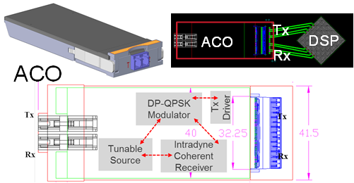 The CFP2-ACO showing the optical building blocks and the electrical connector linking the module to the DSP-ASIC. Source: OIF
The CFP8 occupies approximately the same area as the CFP2 but is not as tall such that the module can be doubled-stacked on a line card for a total of 16 CFP8-ACOs on a line card.
Given that the CFP8 will support up to four carriers per module - each up to 400 gigabit - a future line card could support 25.6 terabits of capacity. This is comparable to the total transport capacity of current leading dense WDM optical transport systems.
Rafik Ward, vice president of marketing at Finisar, says such a belly-to-belly configuration of the modules provides future-proofing for next-generation lineside interfaces. “Having said that, it is not clear when, or how, we will be able to technically support a four-carrier coherent solution in a CFP8 form factor,” says Ward.
Oclaro stresses that such a high total capacity implies that sufficient coherent DSP silicon can fit on the line card. Otherwise, the smaller-height CFP8 module may not enable the fully expected card density if the DSP chips are too large or too power-hungry.
OIF goal
Besides resulting in a higher density module, a key OIF goal of the work is to garner as much industry support as possible to back the CFP8-ACO. “How to create the quantity of scale so that deployment becomes less expensive and therefore quicker to implement,” says Gass.
The OIF expects the work to be similar to the development of the CFP2-ACO Implementation Agreement. But one desired difference is to limit the classes associated with the module. The CFP2-ACO has three class categories based on whether the module has a limited and linear output. “The goal of the CFP8-ACO is to limit the designs to single classes per wavelength count,” says Gass.
Gass is looking forward to the CFP8-ACO specification work. Certain standards efforts largely involve making sure components fit into a box whereas the CFP8-ACO will be more engaging. “This project is going to drive innovation and that will drive some technical work,” says Gass.