
How scaling optical networks is soon to change
Carrier division multiplexing and spatial division multiplexing (CSDM) are both needed, argues Lumentum’s Brian Smith.
The era of coherent-based optical transmission as is implemented today is coming to an end, argues Lumentum in a White Paper.

Brian Smith
The author of the paper, Brian Smith, product and technology strategy, CTO Office at Lumentum, says two factors account for the looming change.
One is Shannon’s limit that defines how much information can be sent across a communications channel, in this case an optical fibre.
The second, less discussed regarding coherent-based optical transport, is how Moore’s law is slowing down.
”Both are happening coincidentally,” says Smith. “We believe what that means is that we, as an industry, are going to have to change how we scale capacity.”
Accommodating traffic growth
A common view in telecoms, based on years of reporting, is that internet traffic is growing 30 per cent annually. The CEO of AT&T mentioned over 30 per cent traffic growth in its network for the last three years during the company’s last quarterly report of 2023.
Smith says that data on the rate of traffic growth is limited. He points to a 2023 study by market research firm TeleGeography that shows traffic growth is dependent on region, ranging from 25 to 45 per cent CAGR.
Since the deployment of the first optical networking systems using coherent transmission in 2010, almost all networking capacity growth has been achieved in the C-band of a fibre, which comprises approximately 5 terahertz (THz) of spectrum.
Cramming more data into the C-band has come about by increasing the symbol rate used to transmit data and the modulation scheme used by the coherent transceivers, says Smith.
 The current coherent era – labelled the 5th on the chart – is coming to an end. Source: Lumentum.
Pushing up baud rate
Because of the Shannon limit being approached, marginal gains exist to squeeze more data within the C-band. It means that more spectrum is required. In turn, the channel bandwidth occupied by an optical wavelength now goes up with baud rate such that while each wavelength carries more data, the capacity limit within the C-band has largely been reached.
Current systems use a symbol rate of 130-150 gigabaud (GBd). Later this year Ciena will introduce its 200GBd WaveLogic 6e coherent modem, while the industry has started work on developing the next generation 240-280GBd systems.
Reconfigurable optical add-drop multiplexers (ROADMs) have had to become ‘flexible’ in the last decade to accommodate changing channel widths. For example, a 400-gigabit wavelength fits in a 75GHz channel while an 800-gigabit wavelength fits within a 150GHz channel.
Another consequence of Shannon’s limit is that the transmission distance limit for a certain modulation scheme has been reached. Using 16-ary quadrature amplitude modulation (16-QAM), the distance ranges from 800-1200km. Doubling the baud rate doubles the data rate per wavelength but the link span remains fixed.
“There is a fundamentally limit to the maximum reach that you can achieve with that modulation scheme because of the Shannon limit,” says Smith.
At the recent OFC show held in March in San Diego, a workshop discussed whether a capacity crunch was looming.
The session’s consensus was that, despite the challenges associated with the latest OIF 1600ZR and ZR+ standards, which promise to send 1.6 terabits of data on a single wavelength, the industry is confident that it will meet the OIF’s 240-280+ GBd symbol rates.
However, in the discussion about the next generation of baud rate—400-500GBd—the view is that while such rates look feasible, it is unclear how they will be achieved. The aim is always to double baud rate because the increase must be meaningful.
“If the industry can continue to push the baud rate, and get the cost-per-bit, power-per-bit, and performance required, that would be ideal,” says Smith.
But this is where the challenges of Moore’s law slowing down comes in. Achieving 240GBd and more will require a coherent digital signal processor (DSP) made using a 3nm CMOS process at least. Beyond this, transistors start to approach atomic scale and the performance becomes less deterministic. Moreover, the development costs of advanced CMOS processes – 3nm, 2nm and beyond – are growing exponentially.
Beyond 240GBd, it’s also going to become more challenging to achieve the higher analogue bandwidths for the electronics and optics components needed in a coherent modem, says Smith. How the components will be packaged is key. There is no point in optimising the analogue bandwidth of each component only for the modem performance to degrade due to packaging. “These are massive challenges,” says Smith.
This explains why the industry is starting to think about alternatives to increasing baud rate, such as moving to parallel carriers. Here a coherent modem would achieve a higher data rate by implementing multiple wavelengths per channel.
Lumentum refers to this approach as carrier division multiplexing.
Capacity scaling
The coherent modem, while key to optical transport systems, is only part of the scaling capacity story.
Prior to coherent optics, capacity growth was achieved by adding more and more wavelengths in the C-band. But with the advent of coherent DSPs compensating for chromatic and polarisation mode dispersion, suddenly baud rate could be increased.
“We’re starting to see the need, again, for growing spectrum,” says Smith. “But now, we’re growing spectrum outside the C-band.”
First signs of this are how optical transport systems are adding the L-band alongside the C-band, doubling a fibre’s spectrum from five to 10THz.
“The question we ask ourselves is: what happens once the C and L bands are exhausted?” says Smith.
Lumentum’s belief is that spatial division multiplexing will be needed to scale capacity further, starting with multiple fibre pairs. The challenge will be how to build systems so that costs don’t scale linearly with each added fibre pair.
There are already twin wavelength selective switches used for ROADMs for the C-band and L-bands. Lumentum is taking a first step in functional integration by combining the C- and L-bands in a single wavelength selective switch module, says Smith. “And we need to keep doing functional integration when we move to this new generation where spatial division multiplexing is going to be the approach.”
Another consideration is that, with higher baud-rate wavelengths, there will be far fewer channels per fibre. And with growing fibre pairs per route, that suggests a future need for fibre-switched networking not just wavelength switching networking as used today.
“Looking into the future, you may find that your individual routeable capacity is closer to a full C-band,” says Smith.
Will carrier division multiplexing happen before spatial division multiplexing?
Smith says that spatial division multiplexing will likely be first because Shannon’s limit is fundamental, and the industry is motivated to keep pushing Moore’s law and baud rate.
“With Shannon’s limit and with the expansion from C-band to C+L Band, if you’re growing at that nominal 30 per cent a year, a single fibre’s capacity will exhaust in two to three years’ time,” says Smith. “This is likely the first exhaust point.”
Meanwhile, even with carrier division multiplexing and the first parallel coherent modems after 240GBd, advancing baud rate will not stop. The jumps may diminish from the doublings the industry knows and that will continue for several years yet. But they will still be worth having.

OFC 2024 industry reflections
Gazettabyte is asking industry figures for their thoughts after attending the recent OFC show in San Diego. In particular, what developments and trends they noted, what they learned and what, if anything, surprised them. Here are the first responses from Huawei, Drut Technologies and Aloe Semiconductor.
Maxim Kuschnerov, Director R&D, Optical & Quantum Communication Laboratory at Huawei.
Some ten years ago datacom took the helm of the optical transceiver market from legacy telecom operators to command a much larger volume of short-reach optics and extend its vision into dense wavelength division multiplexing (DWDM).
At OFC, the industry witnessed another passing-of-the-torch moment as Nvidia took over the dominant position in the optics market where AI compute is driving optical communication. The old guard of Google is now following while others are closely watching.
Nvidia’s Blackwell NVL72 architecture was the talk of the conference and its exclusive reliance on passive copper cables for intra-rack GPU-to-GPU interconnects dampened the hopes of Wall Street optics investors at the show.
Since the copper backplane is using 224-gigabit serdes, last year’s hot topics of 100 gigabit-based linear pluggable optics or dense optical interconnects based on 16×100 gigabits suddenly felt dated and disconnected from where the market already is. It is also in no shape to respond to where the compute market is rapidly going next: 400-gigabit-per-lane signalling.
Here, the main question is which type of connectivity for the GPU scale-up in the intra-rack domain would be employed and whether this might be the crossover point to go to optical cables? But as often is the case in the optical business, one should never fully bet against CMOS and copper.
The long-term evolution of AI compute will impact optical access and this was also a theme of some of the OFC panels.
6G is envisioned to be the first wireless network supporting devices primarily, not humans, and it’s fair to assume that a majority of those distributed devices will be AI-enabled. Since it will be uneconomical to send the raw training or inference bandwidth to the network core, the long term evolution of AI compute might see a regionalisation and a distribution towards the network edge, where there would be a strong interdependence of 6G, fronthaul/ backhaul & metro edge networks, and the AI edge compute cloud.
While a majority of coherent PON presentations failed to quantify the market driver for introducing the more expensive technology in future access networks, AI-data powered 6G fronthauling over installed optical distribution networks will drive the bandwidth need for this technology, while residential fibre-to-the-home – “PON for humans” – can still evolve to 200 gigabit using low cost intensity modulation direct detection (IMDD) optics.
The times are over where the talk of cheaper datacom ZR optics dominated the show and commanded attendance at the Market Watch sessions. Don’t misunderstand, the step to 1600ZR is technologically important and market-relevant, but since coherent doesn’t have “AI” written all over it, the ZR evolution was more a footnote of the exhibition. However, in a necessary move away from electro-absorption-modulated lasers (EMLs), 400-gigabit-per-lane optics for intensity modulation direct detection will share similar Mach-Zehnder modulator structures as coherent optics.
Thus, start-ups crowding the thin-film lithium niobate modulator market in the US, Europe and China are going for both: the coherent and the intensity modulation direct detection dollar.
Meanwhile, the established silicon photonics ecosystem will have to wrap its head around what their value-add in this domain will be since silicon photonics would be just the carrier of other materials enabling lasers, modulators and photodetectors.
Bill Goss, CEO of Drut Technologies
The last time I attended OFC, the conference was in Los Angeles at the Staples Center.
One thing I found super interesting at this year’s event was the number of companies working on optically-connected memory solutions. But the biggest noteworthy item to us was a number of presentations on using optical circuit switching (OCS) for AI/ML workloads.
Nvidia and some universities presented projects using OCS in the data centre and Coherent actually showed a new 300×300 switch in their booth. There also seemed to be a feeling that the world has been waiting on co-packaged optics for years.
One thing evident in talking with optical companies that typically focus on service provider networks, is that they all want to get inside the data centre. That is where the big market explosion is going to be in the next decade and companies are thinking about how to gain share in the data centre with optical solutions.
You could almost feel the gloom around service provider capital expenditure and the companies that normally play in this market are looking at all the spending going on inside the data centre and trying to figure out how to access this spend.
Drut Technologies did not exhibit at OFC. Instead, we used the show to listen to presentations and talk to suppliers and customers. Surprises were the amount of pluggable optics available.
Walking through the show floor, it seemed like a sea of pluggables and I had multiple meetings with companies looking to put coherent optics inside the data centre. Visually too, the amount of pluggables was noticeable.
I was also surprised at the absence of certain companies. It seems companies opted for a private meeting room rather than a booth. I do not know what that means, if anything, but if the trend continues, the show floor is going to be half-filled with private meeting spaces. It will be like walking through a maze of white walls.
I was not surprised with all the AI excitement, but the show did not seem to have a lot of energy.
Chris Doerr, CEO of Aloe Semiconductor
The first most noteworthy trend of this OFC was the acceleration of pluggable module data rates. There were demonstrations of 1.6-terabit pluggables by almost every module vendor. This was supposed to be the year of 800 gigabit not 1.6 terabit.
Digging into it more, most of the demonstrated 1.6 terabit modules were not fully operational – the receiver was not there, all the channels not running simultaneously, etc. – but some EML-based modules were complete.
The second most noteworthy trend was supply constraint and the subsequent driving of new technology. For example, it was said that Nvidia bought up all the VCSEL supply capacity. This is driving up VCSEL prices and seems to be allowing a surge of silicon photonics in the lower speed markets that were previously thought to be done and closed, such as active optical cables. There was an increasing polarity in opinion on linear pluggable optics, with opposing opinions by well-known technologists.
It seems that Nvidia is already deploying 100 gigabit per lane linear pluggable optics, and Arista will be deploying it soon. For 200 gigabit per lane, it seems the trend is to favour half-linear pluggable optics, or linear receive optics (LRO), in which the transmit is still retimed.
Large-scale co-packaged optics (not to be confused with small-scale CPO of a coherent ASIC and coherent optics) was exhibited by more vendors this year. It seems very little, if any, is deployed. Large-scale CPO is inevitable, but it on a significantly slower time scale than previously thought.
For 200 gigabit per lane, there were many demonstrations using EMLs and quite a few using silicon photonics. Most of the silicon photonics demonstrations seemed to require driver ICs to overcome the reduced modulation efficiency, sacrificed to achieve the higher bandwidth. Consequently, most companies appear to be throwing in the towel on silicon photonics for 200 gigabaud (GBd) applications, instead moving toward indium phosphide and thin-film LiNbO3 (TFLN). This is surprising.
This author strongly believes in the trend usually followed by silicon electronics in that innovation will allow silicon photonics to achieve 200GBd. It is unreasonable to expect indium phosphide or TFLN to meet the volumes, density, and pricepoints required for 3.2-terabit modules and beyond.
There is no widely accepted solution for 400-gigabit-per-lane intensity modulation direct detection. Proposals include two wavelengths x 200 gigabit, going for 200GBd early, and dual-polarization intensity modulation direct detection.
There was significant discussion about optoelectronic interposers, with start-ups LightMatter and Celestial AI receiving large funding in this area. However, the end customers do not seem to have a need for this technology, so it is unclear where it is headed.
OFC was highly noteworthy this year, driven by the surging demand for high-performance computing interconnects. Probably the biggest takeaway is the amount of uncertainty and polarised views, including linear pluggable optics, silicon-photonic’s future, and optoelectronic interposers.

Teramount’s scalable fibre-attach for co-packaged optics
 Part 2: Co-packaged optics: fibre-attach
Hesham Taha recently returned from a trip to the US to meet with leading vendors and players serving the silicon photonics industry.
“It is important to continue probing the industry,” says Taha, the CEO of start-up Teramount.
Teramount specialises in fibre assembly technology: coupling fibre to silicon photonics chips.
Taha is now back in the US, this time to unveil Teramount’s latest product at this week’s OFC show being held in San Diego. The company is detailing a new version of its fibre assembly technology, dubbed Teraverse-XD, that doubles the density of fibres connected to a silicon photonics chip.
Teramount is also announcing it is working with GlobalFoundries, a leading silicon-photonics foundry.
Connecting fibre to a silicon photonics device for a pluggable optical module is straightforward. However, attaching fibre to an optical engine for co-packaged optics is challenging. The coupling must be compact and scale to enable even denser connections in future. This is especially true with the co-packaging of future 100-terabit and 200-terabit Ethernet switch chips.
“If I were to describe the last year, it would be aligning our [Teramount] activities to the industry’s evolving needs,” says Taha. “A key part of those needs is being driven by optical activities for AI applications.”
Edge versus surface coupling
Companies are pursuing two main approaches to connecting fibre to a silicon photonics device: surface and edge (side) coupling.
Surface coupling – or its academic term, off-plane coupling – deflects light vertically, away from the chip’s surface. In contrast, edge (in-plane) or side coupling sends the optical waveguide’s light straight through to the fibre at the chip’s edge.
A silicon-photonics grating coupler is used for surface coupling, glancing the light away from the chip’s plane. However, the grating coupler is wavelength-dependent such that the angle of the defection varies with the light.
In contrast, side coupling is wideband. “You can carry multiple wavelengths on each channel,” says Taha. However, side coupling has limited interfacing space, referred to as ‘shoreline density’.
Side coupling is also more complicated to manufacture in volume. Directly bonding the fibre to the chip involves adhesive, and the fibres get in the way of reflow soldering. “It [side coupling] is doable for transceivers, but to make co-packaged optics, side coupling becomes complicated,” says Taha.
Teramount’s approach
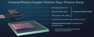
Teramount’s approach couples the fibre to the silicon photonics chip using two components: a photonic plug and a photonic bump.
The photonic plug holds the fibres and couples them to the silicon photonics chip via the photonic bump, a component made during the silicon photonics wafer processing. The photonic bump consists of two elements: a wideband deflector and a lens mirror for beam expansion. Expanding the light beam enables much larger assembly tolerances: +/- 30 microns. And across this 60-micron window, only half a dB is lost in misalignment tolerances.
The resulting wafer-level manufacturing may be more complicated, says Taha, but the benefit is relaxed tolerances in the assembly, wide-band surface coupling, and when testing the wafer and the die.
The photonic bump-and-plug combination also enable detachable optics for co-packaged optics designs. This benefits manufacturing and is wanted for co-packaged optics.
Teraverse and Teraverse-XD
There is a clear demarcation between the optics and the switch chip when using pluggables in the data centre. In contrast, co-packaged optics is a system with the optics embedded alongside the chip. A vendor may work with multiple companies to make co-packaged optics, but one product results, with the chip and optical engined co-packaged.
Teramount’s Teraverse solution, using the plug-and-bump combination, brings pluggability to co-packaged optics. The fibres can be attached and detached from the optical engines. “It’s very important to keep that level of pluggability for co-packaged optics,” says Taha.
The approach also benefits manufacturing yield and testing. Separating the fibres from the package protects the fibres during reflow soldering. “Ideally, you want the fibre connected at the last stage and still maintain high level of testability during the packaging process,” says Taha.
Detachable fibre also brings serviceability to co-packaged optics, benefitting for data centre operators.
Teraverse, Teramount’s detachable fiber-to-chip interface, supports single-mode fiber with 125-micron diameter at a 127-micron pitch separation.

Teraverse-XD, announced for OFC, is a follow-on that doubles the fibre density to achieve a near 64-micron pitch. Here, fibres are placed on top of each other, scaling in the Z-dimension. The approach is like how rods or pipes are stored, with the second row of fibres staggered, sitting in the valleys between adjacent fibers in the lower row.
Two rows of photonic bumps are used to couple the light to each row of fibres (see image above). “It’s very important to keep the same real-estate but to have twice the number of fibres,” says Taha.
Future scaling is possible by adding more rows of fibres or by adopting fibres with a smaller pitch.
Teramount’s technology also supports both edge coupling and surface coupling. “We are agnostic,” says Taha. If a co-packaged optics or optical engine vendor wants to use side coupling, it can use the bump-and-plug combination. The bump deflects the beam upwards to the plug packaging which takes the fibres and sends them out horizontally. “We are converting edge coupling to wideband surface coupling,” says Taha. “You don’t need to sacrifice bandwidth to do surface coupling.”
If the vendor wishes to use a grating coupler, Teramount’s bump-and-plug supports that, too, enabling detachable fibering. But here, only the bump’s expanding mirror is used. “For the wideband surface coupling cased, the bump uses two components: the deflector and the expanding mirror,” says Taha.
Both cases are supported by what Teramount refers to as its Universal Photonic Coupler, shown.
Market expectations
Despite being discussed for over a decade, Taha is not surprised that data centre operators have yet to adopt co-packaged optics.
He points out that hyperscalers only want to use co-packaged optics for Ethernet switches once the technology is more mature. They can also keep using a proven alternative: pluggable modules, that continue to advance.
“Hyperscalers are not against the technology, but it is not mature enough,” says Taha. Hyperscalers and systems vendors also want an established supply chain and not proprietary solutions.
To date, Broadcom’s first co-packaged optics switch solution at 25.6-terabit was adopted by Tencent. Broadcom has announced for OFC that it is now delivering its latest 51.2-terabit Bailly co-packaged optics design, backed by ByteDance.
“AI is a different story,” says Taha. “This is the tipping point for a leading vendor to start taking seriously co-packaged optics.”
The advantage of co-packaged optics here is that it accommodates the reach – radix -as well as power savings and improved latency.
Taha expects initial volumes of co-packaged optics sales in 2026.

A coherent roadmap for co-packaged optics
Is coherent optics how co-packaged will continue to scale? Pilot Photonics certainly thinks so.

Part 1: Co-packaged optics
Frank Smyth, CTO and founder of Pilot Photonics, believes the firm is at an important inflection point.
Known for its comb laser technology, Pilot Photonics has just been awarded a €2.5 million European Innovation Council grant to develop its light-source technology for co-packaged optics.
The Irish start-up is also moving to much larger premises and is on a recruitment drive. “Many of our projects and technologies are maturing,” says Smyth.
Company
Founded in 2011, the start-up spent its early years coupled to Dublin City University. It raised its first notable investment in 2017.
The company began by making lab instrumentation based on its optical comb laser technology which emits multiple sources of light that are frequency- and phased-locked. But a limited market caused the company to pivot, adding photonic integration to its laser know-how.
Now, the start-up has a fast-switching, narrow-linewidth tunable laser, early samples of which are being evaluated by several “tier-one” companies.
Pilot Photonics also has a narrowband indium-phosphide comb laser for optical transport applications. This will be the next product it samples.
More recently, the start-up has been developing a silicon nitride-based comb laser for a European Space Agency project. “The silicon nitride micro-resonator in the comb is a non-linear element that enables a very broad comb for highly parallel communication systems and for scientific applications,” says Smyth. It is this laser type that is earmarked for the data centre and for co-packaged optics applications.
Smyth stresses that while still being a small company, the staff has broad expertise. “We cover the full stack,” he says.
Skills range from epitaxial wafer design, photonic integrated circuit (PIC)s and lasers, radio frequency (RF) and thermal expertise, and digital electronics and control design capabilities.
“We learned early on that it’s all well making a PIC, but if no one can interface to it, you are wasting your time,” says Smyth.
Co-packaged optics
Co-packaged optics refers to adding optics next to an ASIC that has significant input-output (I/O) data requirements. Examples of applications for co-packaged optics include high-capacity Ethernet switch chips and artificial intelligence (AI) accelerators. The goal is to give the chip optical rather than electrical interfaces, providing system-scaling benefits; as electrical signals get faster, their reach shrink.
The industry has been discussing co-packaged optics for over a decade. Switch-chip players and systems vendors have shown prototype designs and even products. And more than half a dozen companies are developing the optical engines that surround, and are packaged with, the chip.
However, the solutions remain proprietary, and while the OIF is working to standardise co-packaged optics, end users have yet to embrace the technology. In part, this is because pluggable optical modules continue to advance in data speeds and power consumption, with developments like linear-drive optics.
The ecosystem supporting co-packaged optics is also developing. Hyperscalers will only deploy co-packaged optics in volume when reliability and a broad manufacturing base are proven.
Yet industry consensus remains that optical I/O is a critical technology and that deployments will ramp up in the next two years. Ethernet switch capacity doubles every two years while AI accelerator chips are progressing rapidly. Moreover, the number of accelerator chips used in AI supercomputers is growing fast, from thousands to tens of thousands.
Pilot Photonics believes its multi-wavelength laser technology, coupled with the intellectual property it is developing, will enable co-packaged optics based on coherent optics to address such scaling issues.
Implementations
Co-packaged optics uses optical chiplets or ‘engines’ that surround the ASIC on a shared substrate. The optical engines typically use an external laser source although certain co-packaged optics solutions such as from Intel and Ranovus can integrate the laser as part of the silicon-photonics based optical engine.
Designers can scale the optical engine’s I/O capacity in several ways. They can increase the number of fibres connected to the optical engine, send more wavelengths down each fibre, and increase the wavelength’s data rate measured in gigabits per second (Gbps).
In co-packaged optics designs, 16 engines typically surround the chip. For a 25.6-terabit Ethernet chip, 16 x 1.6-terabit engines are used, each 1.6-terabit engine sending a 100Gbps DR1 signal per fibre. The total fibres per engine equals 32: 16 for the transmit and 16 for the receive (see table).
| Switch capacity/Tbps | Optical engine/Tbps | Optical engines | Data rate/fibre | No. fibres/ engine* |
| 25.6 | 1.6 | 16 | 100G DR, 500m | 32 |
| 25.6 | 3.2 | 8 | 100G DR, 500m | 64 |
| 51.2 | 6.4 | 8 | 400G FR4, 2km | 32 |
| 102.4 (speculative) | 6.4 | 16 | 400G FR4, 2km | 16 |
| 102.4 (speculation) | 12.8 | 8 | 400G FR4, 2km | 32 |
*Not counting the external laser source fibre.
Broadcom’s co-packaged optical approach uses eight optical engines around its 25.6-terabit Tomahawk 4 switch chip, each with 3.2Tbps capacity. For the Tomahawk 5, 51.2-terabit Bailly co-packaged optics design, Broadcom uses eight, 6.4Tbps optical engines, sending 400-gigabit FR4, or 4-wavelength coarse WDM wavelengths, across each fibre. Using FR4 instead of DR1 halves the number of optical engines while doubling overall capacity.
The co-packaging solutions used in the next-generation 102.4-terabit switch chip are still to be determined. Capacity could be doubled using twice as many fibres, or by using 200-gigabit optical wavelengths based on 112G PAM-4 electrical inputs, twice the speed currently used.
But scaling routes for the generation after that – 204.8-terabit switch chips and beyond – and the co-packaged optics design become unclear due to issues of dispersion and power constraints, says Smyth.
Scaling challenges
Assuming eight engines were used alongside the 200-terabit ASIC , each would need to be 25.6Tbps. The fibre count per engine could be doubled again or more wavelengths per fibre would be needed. One player, Nubis Communications, scales its engines and fibres in a 2D array over the top of the package, an approach suited to fibre-count growth.
Doubling the wavelength count is another option but adopting an 8-wavelength CWDM design with 20nm spacing means the wavelengths would cover 160nm of spectrum. Over a 2km reach, this is challenging due to problems with dispersion. Narrower channel spacings such as those used in the CW-WDM MSA (multi-source agreement) require temperature control to ensure the wavelengths stay put.
Keeping the symbol rate fixed but doubling the data rate is another option. But adopting the more complex PAM-8 modulation brings its own link challenges.
Another key issue is power. Current 51.2-terabit switches require 400mW of laser launch power (4 x 100mW lasers) per fibre and there are 128 transmit fibers per switch.
“Assuming a wall plug efficiency of 20 per cent, that is around 250W of power dissipation just for the lasers,” says Smyth. “Getting to 4Tbps per fibre appears possible using 16 wavelengths, but the total fiber launch power is 10 times higher, requiring 2.5kW of electrical power per switch just for the lasers.”
In contrast, single-polarisation coherent detection of 16-QAM signals through a typical path loss of 24dB could match that 4Tbps capacity with the original 250W of laser electrical power, he says.
 The optimised total laser power improvement for coherent detection versus direct detection as a function of the additional losses in the signal path (the losses not also experienced by the local oscillator). Source: Pilot Photonics
Coherent detection is associated with a high-power digital signal processor (DSP). Are such chips feasible for such a power-sensitive application as co-packaged optics?
Coherent detection adds some DSP complexity, says Smyth, but it has been shown that for pluggable-based intra data centre links using 5nm CMOS silicon, 400-gigabit coherent and direct-detection are comparable in terms of ASIC power but coherent requires less laser power.
“Over time, a similar battle will play out for co-packaged optics. Laser power will become a bigger issue than DSP power,” he says.
The additional signal margin could be used for 10km links, with tens of terabits per fibre and even 80km links at similar per-fibre rates to current direct detection.
“We believe coherent detection in the data centre is inevitable,” says Smyth. “It’s just a question of when.”
Comb-based coherent co-packaged optics
Coherent co-packaged optics brings its own challenges. Coherent detection requires alignment between the signal wavelength and the local oscillator laser in the receiver. Manufacturing tolerances and the effects of ageing in simple laser arrays make this challenging to achieve.
“The wavelengths of a comb laser are precisely spaced, which greatly simplifies the problem,” says Smyth. “And combs bring other benefits related to carrier recovery and lack of inter-channel interference too”.
Pilot Photonics’ comb laser delivers 16 or 32 wavelengths per fibre, up to 8x more than existing solutions. Smyth says the company intends to fit its comb laser inside the OIF’s standardised External Laser Source pluggable form-factor,
The start-up is also developing a coherent ring resonator modulator for its design. The ring modulator is tiny compared with Mach-Zehnder interferometer modulators used for coherent optics.
Pilot Photonics is also developing IP for coherent signal processing. Because its comb laser locks the frequency and phase of the wavelengths generated, the overall control and signal processing can be simplified.
While it will offer the comb laser, the start-up does not intend to develop the DSP IC nor make optical engines itself.
“A strategic partnership with a company with its own manufacturing facilities would be the most effective way of getting this technology to market,” says Smyth.

DustPhotonics raises funding for 800G and 1.6T modules
- DustPhotonics has raised $24 million in funding.
- The start-up has taped out its 200 gigabit-per-lane optical chip.
- DustPhotonics expects the 1.6-terabit module market to ramp, starting year-end.
DustPhotonics, which develops chips for transmit optical sub-assemblies (TOSAs) for 400 and 800-gigabit pluggable optical modules, has raised $24 million. The funding extends its Series B funding round.
“When you start ramping up products, you have to iron out the creases around supply chain, production, and everything else,” says Ronnen Lovinger, CEO of DustPhotonics.
DustPhotonics has several customers and a backlog of orders for its 400 and 800-gigabit photonic integrated circuits (PICs). The company has also taped out its 200 gigabit-per-lane chip and will have products later this year.
800-gigabit PICs
DustPhotonic’s products include the Carmel-4-DR4, a 400-gigabit DR4 PIC, and several variants of its 800-gigabit Carmel-8.
“Most of our customers and engagements are interested in the 800-gigabit applications,” says Lovinger.
DustPhotonics has developed a way of attaching a laser source to its silicon photonics chip with sub-micron accuracy. The company uses standard off-the-shelf continuous-wave lasers operating at 1310nm.
The efficiency of the laser-attach scheme means one laser can power four channels, or two lasers can be used for a DR8 design, reducing cost and power consumption.
At the ECOC show last October, DustPhotonics unveiled three 800-gigabit Carmel-8 products. The products include a DR8 with a reach of 500m, a 2km DR8+, and an 800-gigabit ‘lite’ version that competes with 100-gigabit VCSEL designs and only uses one laser. Several customers are considering the Carmel-8-Lite for Ethernet and PCI Express applications.
Manufacturing
DustPhotonics is working with foundry Tower Semiconductors as it goes to production.
“Having a strong fab partner is very important for silicon photonics,” says Lovinger, who views Tower as a leading silicon photonics foundry. “We have been working with Tower for five years, and they have been a strong partner.” DustPhotonics is using several partners for device assembly.
DustPhotonics is headquartered in Israel and has 50 staff, 37 of whom are in R&D. Investors in the latest funding round include Sienna Venture Capital, Greenfield Partners, Atreides Management, and Exor Ventures.
Lovinger will attend the OFC show later this month for meetings with customers and prospects. “It is always good to see so many customers under the same roof,” he says.
200-gigabit optical
DustPhotonics has a highly stable silicon-photonics modulator that does not need to be temperature-controlled and operates at 200 gigabits per lane.
Developing a 200 gigabit-per-lane transmit chip means that DustPhotonics can address a 4-lane 800-gigabit DR4 and an 8-lane 1.6-terabit DR8 modules.
Lovinger says that many driver and digital signal processing chip companies already offer 800 gigabit/ 1.6-terabit chips. Thus, he sees the advent of 1.6 terabit modules as straightforward once its TOSA design is ready.
“Once we have 200 gigabits-per-lane, it takes us to 1.6 terabits and, in some configurations, 3.2 terabits,” says Lovinger. “We see the 1.6-terabit market starting at the end of this year and ramping in 2025.”
Lovinger says the progress of pluggable modules is postponing the need for co-packaged optics. That said, the company says it has the technologies needed to address co-packaged optics when the market finally needs it.

imec's novel ADC promises faster sampling rates
The analogue-to-digital and digital-to-analogue converters (ADCs/DACs) are like the equals sign in mathematics.
The equals sign is taught as showing two sides of an equation being the same. But really, it is a gateway between two worlds. The same applies to the ADC and DAC, which equate between the analogue and digital worlds.
Progress in wireline communications, whether client-side optics or coherent optical modems at 800 gigabits and soon 1.6 terabits, means converters must sample at higher rates.
In February, at the IEEE International Solid-State Circuits Conference (ISSCC) in San Francisco, imec detailed a proof-of-concept chip design that promises to advance high-speed ADCs.
In the paper, the authors from the Belgium nano and digital technology innovation centre detailed a 16nm CMOS 7-bit ADC test chip operating at 42 Giga-samples per second (GSps). The speed is not particularly noteworthy, but the design is: a tiny ADC circuit that promises future faster designs.
imec believes a 250-300GSps ADC will be possible when implemented in a state-of-the-art 2nm or 3nm CMOS process.
Converters for comms
I am text block. Click edit button to change this text. Lorem ipsum dolor sit amet, consectetur adipiscing elit. Ut elit tellus, luctus nec ullamcorper mattis, pulvinar dapibus leo.
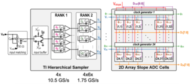
Time-interleaved SAR
For such high-speed ADCs, a time-interleaved successive approximation register (SAR) architecture is commonly used. The converter design is relatively small and power efficient. Van Driessche says imec has almost two decades of experience designing such ADCs.
The time-interleaved refers to the sampled high-speed signal being distributed across parallel ADC channels. Van Driessche cites as an example a 100GSps ADC that distributes the samples to 100 such interleaved channels, each operating at 1GSps.
“The input [to the ADC] is still operating at full speed, but your ADCs, or channels, operate at a hundredth of the speed,” says Van Driessche.
The issue with a time-interleaved SAR-based converter is that as the speed increases, so does size. The result is longer interconnect lines linking the channels and distributing the clocking signal.
“Distributing the signal and the clock over long lines leads to large parasitics,” says Van Driessche. And with parasitics comes a higher power consumption and/or a lower overall analogue bandwidth.
imec’s ISSCC ADC (see diagram) simplifies the SAR circuitry. Dubbed a time-interleaved slope ADC, each channel is even slower than the traditional design. But the primary circuit is tiny, comprising a sampling switch, sampling capacitor, comparator, and a few digital gates. Reducing its size and arranging multiple such units in a 2D array shortens the interconnects, lowering the power and widening the circuit’s bandwidth.
The result is a compact design and a much-reduced power consumption. “This is the essence: to make the core of the ADC significantly smaller, smaller than any alternative that we are aware of,” says Van Driessche.
5nm CMOS design
The ISSCC paper reports the results of a 16nm test chip operating at 42GSps. “You first need to prove that it works,” says Van Driessche. The core’s area is 0.07mm2 only.
Now, imec is working on a 5nm CMOS version. The smaller and faster transistors help achieve higher sampling rates and better power efficiency. But it also comes with challenges: much more impact from parasitics limiting the analogue bandwidth and the resulting speed, and obtaining sufficient output voltage swing at low-power consumption for the DAC.
“The real benefit of the novel ADC architecture comes when you go to higher sampling rates,” says Van Driessche. imec is not saying how fast, but it expects it to exceed 150GSps significantly. Imec expects to tape out the ADC alongside an equivalent DAC next month, with measurement results expected by year-end.
Based on simulation results, imec expects to halve the ADC’s power consumption compared to other similar-speed ADCs. Designers get a notable power saving or can use two channels for the same power.
At OFC 2023, Imec detailed how it expects to achieve sampling rates of 250GSps for a 3nm CMOS coherent DSP design.
How much faster can ADCs go?
Van Driessche says that in future, the gains from technology scaling will diminish, requiring very skilled designers and a huge amount of effort.
“At some point, and I cannot say when, there will be diminishing returns,” he says. “We are not there yet, but we are getting closer.”
Once companies decide that a limit is reached, several parallel channels will be needed, a development designers will want to avoid for as long as possible.

OFC 2024 reflects a mature industry with new offshoots
- The three General Chairs preview the upcoming Optical Fiber Communications (OFC) conference and discuss photonics developments and trends.
- The General Chairs' role is to choose the plenary speakers, programme theme, and conference schedule.
- OFC takes place during March 24th-28th in San Diego, CA.*
Photonics, at least for traditional applications, has become a mature industry. So says Professor Dimitra Simeonidou, one of this year’s OFC General Chairs.
y traditional, Simeonidou is referring to classical optical communications.
But she also stresses new developments: the use of optical fibres for environmental sensing, optics for satellites, and quantum.
“Quantum is like a micro-OFC,” says Simeonidou. “You have issues from technology to subsystem to system applications now appearing in the OFC programmes.”

The OIF's coherent optics work gets a ZR+ rating
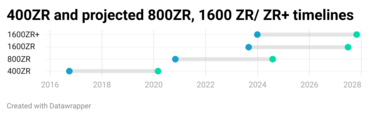
The OIF has started work on a 1600ZR+ standard to enable the sending of 1.6 terabits of data across hundreds of kilometres of optical fibre.The initiative follows the OIF's announcement last September that it had kicked off 1600ZR. ZR refers to an extended reach standard, sending 1.6 terabits over an 80-120km point-to-point link.
600ZR follows the OIF’s previous work standardising the 400-gigabit 400ZR and the 800-gigabit 800ZR coherent pluggable optics.
The decision to address a ‘ZR+’ standard is a first for the OIF. Until now, only the OpenZR+ Multi-Source Agreement (MSA) and the OpenROADM MSA developed interoperable ZR+ optics.
The OIF’s members’ decision to back the 1600ZR+ coherent modem work was straightforward, says Karl Gass, optical vice chair of the OIF’s physical link layer (PLL) working group. Several companies wanted it, and there was sufficient backing. “One hyperscaler in particular said: ‘We really need that solution’,” says Gass.
OIF, OpenZR+, and OpenROADM
Developing a 1600ZR+ standard will interest telecom operators who, like with 400ZR and the advent of 800ZR, can take advantage of large volumes of coherent pluggables driven by hyperscaler demand. However, Gass says no telecom operator is participating in the OIF 1600ZR+ work.
“It appears that they are happy with whatever the result [of the ZR+ work] will be,” says Gass. Telecom operators are active in the OpenROADM MSA.
Now that the OIF has joined OpenZR+ and the OpenROADM MSA in developing ZR+ designs, opinions differ on whether the industry needs all three.
“There is significant overlap between the membership of the OpenZR+ MSA and the OIF, and the two groups have always maintained positive collaboration,” says Tom Williams, director of technical marketing at Acacia, a leading member of the OpenZR+. “We view the adoption of 1600ZR+ in the OIF as a reinforcement of the value that the OpenZR+ has brought to the market.”
Robert Maher, Infinera’s CTO, believes the industry does not need three standards. However, having three organisations does provide different perspectives and considerations.
Meanwhile, Maxim Kuschnerov, director R&D at Huawei, says the OIF’s decision to tackle ZR+ changes things.”OpenZR+ kickstarted the additional use cases in the industry, and OpenROADM took it away but going forward, it doesn’t seem that we need additional MSAs if the OIF is covering ZR+ for Ethernet clients in ROADM networks,” says Kuschnerov. “Only the OTN [framing] modes need to be covered, and the ITU-T can do that.”
Kuschnerov also would like more end-user involvement in the OIF group. “It would help shape the evolving use cases and not be guided by a single cloud operator,” he says.
ZR history
The OIF is a 25-year-old industry organisation with over 150 members, including hyperscalers, telecom operators, systems and test equipment vendors, and component companies.
In October 2016, the OIF started the 400ZR project, the first pluggable 400-gigabit Ethernet coherent optics specification. The principal backers of the 400ZR work were Google and Microsoft. The standard was designed to link equipment in data centres up to 120km apart.
The OIF 400ZR specification also included an un-amplified version with a reach of several tens of kilometres. The first 400ZR specification document, which the OIF calls an Implementation Agreement, was completed in March 2020 (see chart above).
The OIF started the follow-up on the 800ZR specification in November 2020, a development promoted by Google. Gass says the OIF is nearing completion of the 800ZR Implementation Agreement document, expected in the second half of 2024.
If the 1600ZR and ZR+ coherent work projects take a similar duration, the first 1600ZR and 1600ZR+ products will appear in 2027.
Symbol rate and other challenges
Moving to a 1.6-terabit coherent pluggable module using the same modulation scheme – 16-ary quadrature amplitude modulation or 16-QAM – used for 400ZR and 800ZR suggests a symbol rate of 240 gigabaud (GBd).
“That is the maths, but there might be concerns with technical feasibility,” says Gass. “That’s not to say it won’t come together.”
The highest symbol rate coherent modem to date is Ciena’s WaveLogic 6e, which was announced a year ago. The design uses a 3nm CMOS coherent digital signal processor (DSP) and a 200GBd symbol rate. It is also an embedded coherent design, not one required to fit inside a pluggable optical module with a constrained power consumption.
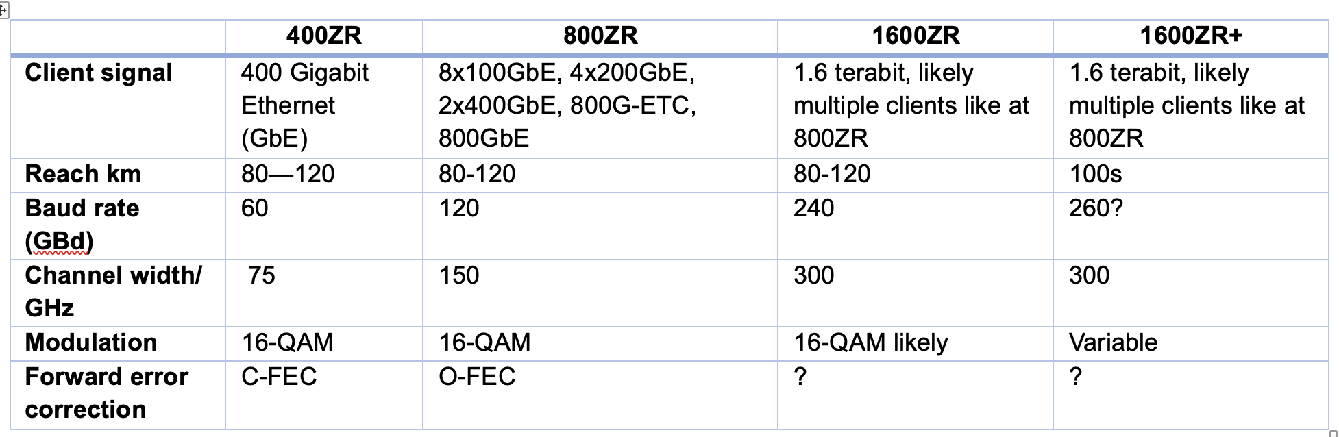
Kuschnerov points out that the baud rates of ZR and ZR+ have differed. And this will likely continue. 800ZR, using Ethernet with no probabilistic constellation shaping, has a baud rate of 118.2GBd, while 800ZR+, which uses OTN and probabilistic constellation shaping, has a baud rate of up to 131.35GBd. Every symbol has a varying probability when probabilistic constellation shaping is used. “This decreases the information per symbol, and thus, the baud rate must be increased,“ says Kuschnerov.
Doubling up for 1600ZR/ ZR+, those numbers become around 236GBd and 262GBd, subject to future standardisation. “So, saying that 1600ZR is likely to be at 240GBd is correct, but one cannot state the same for a potential 1600ZR+,” says Kuschnerov.
Nokia’s view is that for 1600ZR, the industry will look at operating modes that include 16QAM at 240 GBd. Other explored options include 64-QAM with probabilistic constellation shaping at 200GBd and even dual optical carrier solutions with each carrier operating at approximately 130GBd. “However, this last option may be challenging from a power envelope perspective,” says Szilárd Zsigmond, head of Nokia’s optical subsystems group.
In turn, if 1600ZR+ reaches 1,000km distances, the emphasis will be on higher baud rate options than those used for 1600ZR. “This will be needed to enable longer reaches, which will also put pressure on managing power dissipation,” says Zsigmond.
The coherent DSP must also have digital-to-analogue (DACs) and analogue-to-digital converters (ADCs) to sample at least at 240 giga-samples per second. Indeed, the consensus among the players is that achieving the required electronics and optics will be challenging.
“All component bandwidths have to double and that is a significant challenge,” says Josef Berger, associate vice president, cloud optics marketing at Marvell.
The coherent optics – the modulators and receivers – must extend their analogue bandwidth of 120GHz. Infinera is one company that is confident this will be achieved. “Infinera, with our highly integrated Indium Phosphide-based photonic integrated circuits, will be producing a TROSA [transmitter-receiver optical sub-assembly] capable of supporting 1.6-terabit transmission that will fit in a pluggable form factor,” says Maher.
The coherent DSP and optics operating must also meet the pluggable modules’ power and heat limits. “That is an extra challenge here: the development needs to maintain focus on cost and power simultaneously to bring the value network operators need,” says Williams. “Scaling baud rate by itself doesn’t solve the challenge. We need to do this in a cost and power-efficient way.”
Current 800ZR modules consume 30W or more, and since the aim of ZR modules is to be used within Ethernet switches and routers, this is challenging. In comparison, 400ZR modules now consume 20W or less.
“For 800ZR and 800ZR+, the target is to be within the 28W range, and this target is not changing for 1600ZR and 1600ZR+,” says Zsigmond. Coherent design engineers are being asked to double the bit rate yet keep the power envelope constant.
Certain OIF members are also interested in backward compatibility with 800ZR or 400ZR. “That also might affect the design,” says Gass.
Given the rising cost to tape out a coherent DSP using 3nm and even 2nm CMOS process nodes required to reduce power per bit, most companies designing ASICs will look to develop one design for the 1600ZR and ZR+ applications to maximise their return on investment, says Zsigmond, who notes that the risk was lower for the first generations of ZR and ZR+ applications. Most companies had already developed components for long-haul applications that could be optimised for ZR and ZR+ applications.
For 400ZR, which used a symbol rate of 60 GBd, 60-70 GBd optics already existed. For 800 gigabit transmissions, high-performance embedded coherent optics and pluggable, low-power ZR/ZR+ modules have been developed in parallel. “For 1600ZR/ZR+, it appears that the pluggable modules will be developed first,” says Zsigmond. “There will be more technology challenges to address than previous ZR/ZR+ projects.”
The pace of innovation is faster than traditional coherent transmission systems and will continue to reduce cost and power per bit, notes Marvell’s Berger: “This innovation creates technologies that will migrate into traditional coherent applications as well.”
Gass is optimistic despite the challenges ahead: “You’ve got smart people in the room, and they want this to happen.”
OIF's OFC 2024 demo
The OIF has yet to finalise what it will show for the upcoming coherent pluggable module interoperable event at OFC to be held in San Diego in March. But there will likely be 400ZR and 800ZR demonstrations operating over 75km-plus spans and 400-gigabit OpenZR+ optics operating over greater distance spans.
Optical transmission: sending more data over a greater reach
Keysight Technologies' chart plots the record-setting optical transmission systems of recent years.
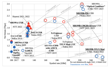
The chart, compiled by Dr Fabio Pittalá, product planner, broadband and photonic center of excellence at Keysight, is an update of one previously published by Gazettabyte.
The latest chart adds data from last year’s conferences at OFC 2023 and ECOC 2023. And new optical transmission achievements can be expected at the upcoming OFC 2024 show, to be held in San Diego, CA in March.
Using LED-based parallelism for fast optical interconnects
Avicena Tech has demonstrated what it claims is the world's smallest one terabit optical transceiver. And the company will reveal more about how it is advancing its optical technology for volume production at the upcoming OFC event in San Diego in March.

The interface technology uses compact light emitting diodes (LED). The interface uses an array of these microLEDs that emit light vertically into a bundle of multimode optical fibres.
Avicena demonstrated its 1 terabit-per-second (Tbps) interface at the recent Supercomputing 23 show in Colorado last November. Its interface used 304 LED-based optical channels, each carrying 3.3 gigabit-per-second (Gbps) of data for a total bandwidth of one terabit.
The transceiver design dubbed LightBundle comprises a small 16nm CMOS process chip. Measuring 3mm x 4 mm, the chip hosts the electrical interface and the optical circuitry. These include the microLEDs, each one less that 10 microns in diameter, that emit blue light.
The LEDs are arranged in 2D arrays that are flip-chipped and bonded onto the chip. The photo-detectors are also arranged in an array and connected to the LEDs via the multimode fibres.
“On the electrical side [of the Lightbundle chip], you can put any interface you want,” says Christoph Pfistner, vice president of sales and marketing at Avicena. The ASIC uses the Open Compute Project’s OpenHBI interface for the electrical interface.
The choice of OpenHBI was due to a hyperscaler customer request. But Avicena plans to use the UCIe chiplet interface for future designs.
Performance metrics
MicroLEDs offer another category of optical interfaces alongside pluggable optical modules, on-board optics, and co-packaged optics (see chart below).
Pfistner stresses that the microLED approach is complementary and does not directly compete with silicon photonics.
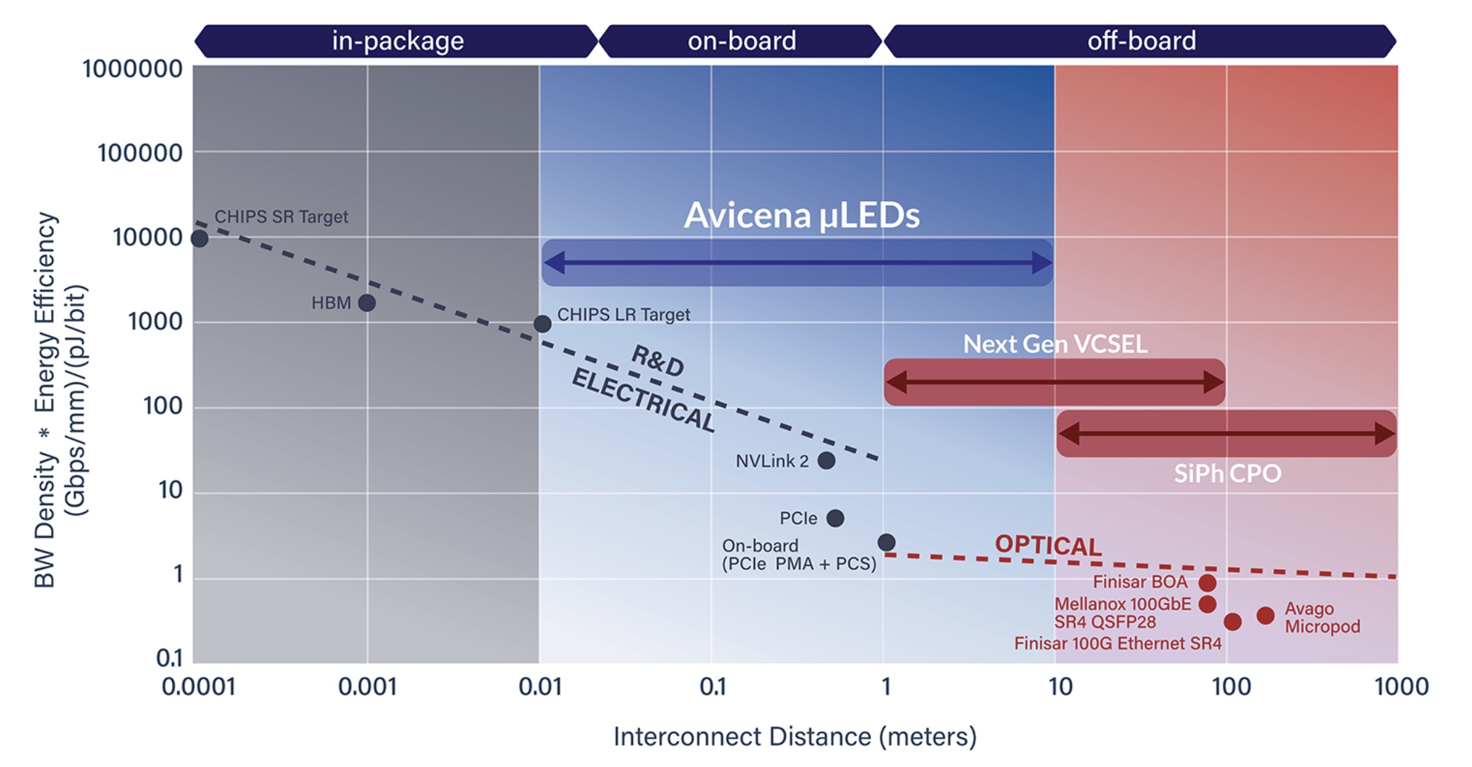
The microLEDs and multimode fibre result in a shorter reach interface – up to 10m – whereas silicon photonics interfaces cover a wider span. MicroLED technology is thus ideal for chip-to-chip applications such as interfacing graphics processor units (GPUs) with high-bandwidth memory (HBM). The microLED technology also benefits intra-rack links.
That said, Pfistner is keen to highlight the technology’s benefits. First, there is no need for an external laser source, and the link consumes fewer picoJoules-per-bit (pJ/b). Avicena says the channel consumes 1pJ/b and says its roadmap suggests sub-pJ/b interface energy consumption. Silicon photonics interfaces typically consume 3-5pJ/b, although the performance metric should also include the extranal laser source.
Like silicon photonics, the LED-based solution can send significant bandwidth across a small length of the chip’s edge, referred to as ‘beachfront’ density. Pfistner says the company can achieve more than 10Tbps/mm interface densities, with the company’s roadmap potentially going to 25Tbps/mm.
Given that this technology is multimode, there is also a relaxed tolerance – a few microns – to coupling the LED light source to the fibre bundle. This is a much more relaxed tolerance than single-mode fibre designs, which require sub-micron precision. More relaxed laser manufacturing tolerances means lower production costs.
The LED-based interface technology can also operate at over 150°C, much higher than traditional lasers. Operating temperatures up to 290°Chave been demonstrated in collaboration with Fred Kish’s North Carolina State University (NCSU) group, says Pfistner.
And since the chip supports non-return-to-zero (NRZ) signalling over short-reach spans, it has a latency advantage compared to optical interfaces requiring signal processing and error correction schemes to close links.
High bandwidth memory
Longer term, Avicena is eyeing the HBM opportunity. HBM uses stacked high-speed memory dies, with several HBMs seated around a processor IC. There is an ongoing race to stack more data in the HBM, overall memory for the processor such as GPUs, and faster data access speeds.
However, HBM has several constraints. First, only so many chips can be stacked on each other in part due to heat dissipation issues. The memory chip at the bottom of the stack must dissipate its heat through all the chips above it, and hot HBM stacks require frequent refresh cycles to retain data, which limits usable bandwidth.
One merit of HBM is that it uses a large bus – 1024 electrical channels wide, each at 6.4 Gbps (HBM3). This is ideal for Avicena’s microLED optical interface. HBM3E memory uses an even faster interface speed of 9.6Gbps. Meanwhile, HBM4, expected in a couple of years, aims to widen the electrical bus from 1024 to 2048 lanes to keep GPU designs fed with data.
Another issue is the size of the stacks relative to the large ASIC chip, such as a GPU. A finite chip size means only so many HBM can surround the ASIC. Due to space limits, high-end GPUs are limited to six HBMs, three stacks on each side of the chip.
Using an optical interface promises larger-capacity high-bandwidth memory designs where the stacks don’t have to be crammed around the ASIC. The memory can be located further away but still be accessible with low latency and energy consumption.
The ASIC-to-HBM interface is thus an important opportunity for short-reach optical interconnects. Moreover, two investors in Avicena are Samsung and Micron, leading memory suppliers.
Avicena’s is now focussed on preparing customer demo kits and increasing its yields before it ramps production for the first product, topics it will be discussing at OFC 2024.