
Marvell kickstarts the 800G coherent pluggable era
Marvell has become the first company to provide an 800-gigabit coherent digital signal processor (DSP) for use in pluggable optical modules.
The 5nm CMOS Orion chip supports a symbol rate of over 130 gigabaud (GBd), more than double that of the coherent DSPs for the OIF’s 400ZR standard and 400ZR+.
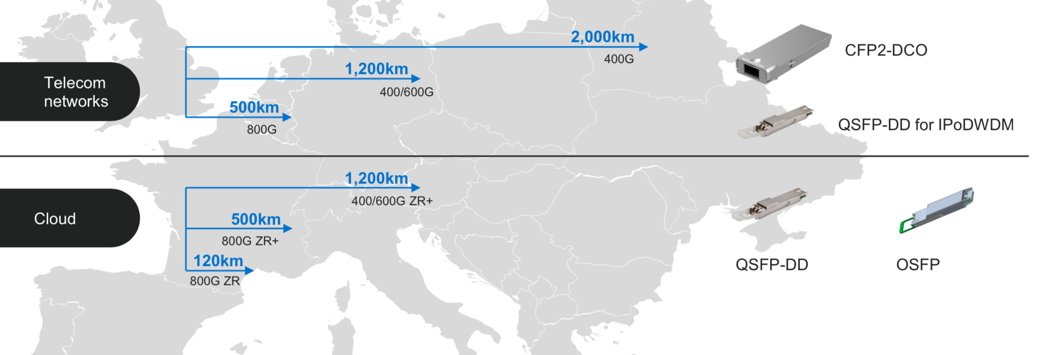
Meanwhile, a CFP2-DCO pluggable module using the Orion can transmit a 400-gigabit data payload over 2,000km using the quadrature phase-shift keying (QPSK) modulation scheme.
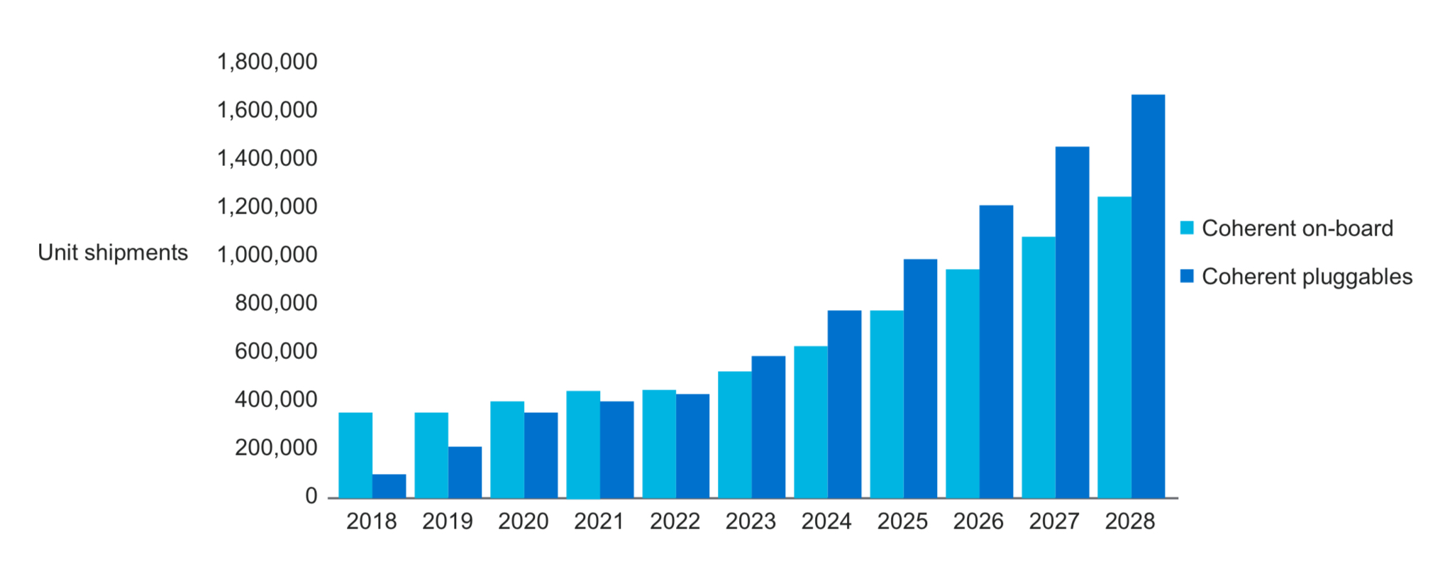
The Orion DSP announcement is timely, given how this year will be the first when coherent pluggables exceed embedded coherent module port shipments.
“We strongly believe that pluggable coherent modules will cover most network use cases, including carrier and cloud data centre interconnect,” says Samuel Liu, senior director of coherent DSP marketing at Marvell.
Marvell also announced its third-generation ColorZ pluggable module for hyperscalers to link equipment between data centres. The Orion-based ColorZ 800-gigabit module supports the OIF’s 800ZR standard and 800ZR+.
Fifth-generation DSP
The Orion chip is a fifth-generation design yet Marvell’s first. First ClariPhy and then Inphi developed the previous four generations.
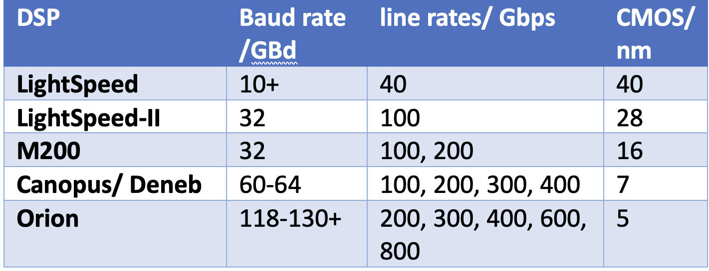
Inphi bought ClariPhy for $275 million in 2016, gaining the first two generation devices: the 40nm CMOS 40-gigabit LightSpeed chip and a 28nm CMOS 100- and 200-gigabit Lightspeed-II coherent DSP products. The 28nm CMOS DSP is now coming to the end of its life, says Liu.
Inphi added two more coherent DSPs before Marvell bought the company in 2021 for $10 billion. Inphi’s first DSP was the 16nm CMOS M200. Until then, Acacia (now Cisco-owned) had been the sole merchant company supplying coherent DSPs for CFP2-DCOs pluggable modules.
Inphi then delivered the 7nm 400-gigabit Canopus for the 400ZR market, followed a year later by the Deneb DSP that supports several 400-gigabit standards. These include 400ZR, 400ZR+, and standards such as OpenZR+, which also has 100-, 200-, and 300-gigabit line rates and supports the OpenROADM MSA specifications. “The cash cow [for Marvell] is [the] 7nm [DSPs],” says Liu.
The Inphi team’s first task after the acquisition was to convince Marvell’s CEO and its chief financial officer to make the most significant investment in a coherent DSP. Developing Orion cost between $100M-300M.
“We have been quiet for the last two years, not making any coherent DSP announcements,” says Liu. “This [the Orion] is the one.”
Marvell views being first to market with a 130GBd-plus generation coherent DSP as critical given how pluggables, including the QSFP-DD and the OSFP form factors, account for over half of all coherent ports shipped.
“It is very significant to be first to market with an 800ZR plug and DSP,” says Jimmy Yu, vice president at market research firm Dell’Oro Group. “I expect Cisco/Acacia to have one available in 2024. So, for now, Marvell is the only supplier of this product.”
Yu notes that vendors such as Ciena and Infinera have had 800 Gigabit-per-second (Gbps) coherent available for some time, but they are for metro and long-haul networks and use embedded line cards.
Use cases
The Orion DSP addresses hyperscalers’ and telecom operators’ coherent needs. The DSP also implements various coherent standards to ensure that the vendors’ pluggable modules work with each other.
Liu says a DSP’s highest speed is what always gets the focus, but the Orion also supports lower line rates such as 600, 400 and 200Gbps for longer spans.
The baud rate, modulation scheme, and the probabilistic constellation shaping (PCS) technique are control levers that can be varied depending on the application. For example, 800ZR uses a symbol rate of only 118GBd and the 16-QAM modulation scheme to achieve the 120km specification while minimising power consumption. When performance is essential, such as sending 400Gbps over 2,000km, the highest baud rate of 130GBd is used along with QPSK modulation.
China is one market where Marvell’s current 7nm CFP2-DCOs are used to transport wavelengths at 100Gbps and 200Gbps.
Using the Orion for 200-gigabit wavelengths delivers an extra 1dB (decibel) of optical signal-to-noise ratio performance. The additional 1dB benefits the end user, says Liu: they can increase the engineering margin or extend the transmission distance. Meanwhile, probabilistic constellation shaping is used when spectral efficiency is essential, such as fitting a transmission within a 100GHz-width channel.
Liu notes that the leading Chinese telecom operators are open to using coherent pluggables to help reduce costs. In contrast, large telcos in North America and Europe use pluggables for their regional networks. Still, they prefer embedded coherent modems from leading systems vendors for long-haul distances greater than 1,000km.
Marvell believes the optical performance enabled by its 130GBd-plus 800-gigabit pluggable module will change this. However, all the leading system vendors have all announced their latest generation embedded coherent modems with baud rates of 130GBd to 150GBd, while Ciena’s 200GBd 1.6-terabit WaveLogic 6 coherent modem will be available next year.
The advent of 800-gigabit coherent will also promote IP over DWDM. 400ZR+ is already enabling the addition of coherent modules directly to IP routers for metro and metro regional applications. An 800ZR and 800ZR+ in a pluggable module will continue this trend beyond 400 gigabit to 800 gigabits.
The advent of an 800-gigabit pluggable also benefits the hyperscalers as they upgrade their data centre switches from 12.8 terabits to 25.6 and 51.2 terabits. The hyperscalers already use 400ZR and ZR+ modules, and 800-gigabit modules, which is the next obvious step. Liu says this will serve the market for the next four years.
Fujitsu Optical Components, InnoLight, and Lumentum are three module makers that all endorsed the Orion DSP announcement.
ColorZ 800 module
In addition to selling its coherent DSPs to pluggable module and equipment makers, Marvell will sell to the hyperscalers its latest ColorZ module for data centre interconnect.
Marvell’s first-generation product was the 100-gigabit coherent ColorZ in 2016 and in 2021 it produced its 400ZR ColorZ. Now, it is offering an 800-gigabit version – ColorZ 800 – to address 800ZR and 800ZR+, which include OpenZR+ and support for lower speeds that extend the reach to metro regional and beyond.

“We are first to market on this module, and it is now sampling,” says Josef Berger, associate vice president of marketing optics at Marvell.
Marvell addressing its module for the hyperscaler market rather than telecoms makes sense, says Yu, as it is the most significant opportunity.
“Most communications service providers’ interest is in having optical plugs with longer reach performance,” says Dell’Oro’s Yu. “So, they are more interested in ZR+ optical variants with high launch power of 0dBm or greater.”
Marvell notes a 30 per cent cost and power consumption reduction for each generation of ColorZ pluggable coherent module.
Liu concludes by saying that designing the Orion DSP was challenging. It is a highly complicated chip comprising over a billion logic gates. An early test chip of the Orion was used as part of a Lumentum demonstration at the OFC show in March.
The ColorZ 800 module will start being sampled this quarter.
What follows the Orion will likely be a 1.6-terabit DSP operating at 240GBd. The OIF has already begun defining the next 1.6T ZR standard.

ECOC 2023 industry reflections
Gazettabyte is asking industry figures for their thoughts after attending the recent ECOC show in Glasgow. In particular, what developments and trends they noted, what they learned and what, if anything, surprised them. Here are the first responses from BT, Huawei, and Teramount.
Andrew Lord, Senior Manager, Optical Networks and Quantum Research at BT
I was hugely privileged to be the Technical Co-Chair of ECOC in Glasgow, Scotland and have been working on the event for over a year. The overriding impression was that the industry is fully functioning again, post-covid, with a bumper crop of submitted papers and a full exhibition. Chairing the conference left little time to indulge in content. I will need to do my regular ECOC using the playback option. But specific themes struck me as interesting.
There were solid sessions and papers around free space optics, including satellite. The activities here are more intense than we would typically see at ECOC. This reflects a growing interest and the specific expertise within the Scottish research community. Similarly, more quantum-related papers demonstrated how quantum is integrating into the mainstream optical industry.
I was impressed by the progress towards 800-gigabit ZR (800ZR) pluggables in the exhibition. This will make for some interesting future design decisions, mainly if these can be used instead of the increasingly ubiquitous 400 gigabit ZR. I am still unclear whether 800-gigabit coherent can hit the required power consumption points for plugging directly into routers. The costs for these plugs, driven by volumes, will have a significant impact.
I also enjoyed a lively and packed rump session debating the invasion of artificial intelligence (AI) into our industry. I believe considerable care is needed, particularly where AI might have a role in network management and optimisation.
Maxim Kuschnerov, Director R&D at Huawei
ECOC usually has fewer major announcements than the OFC show. But ECOC was full of technical progress this time, making the OFC held in March seem a distant memory.
What was already apparent in September at the CIOE in Shenzhen was on full display on the exhibition floor in Glasgow: the linear drive pluggable optics (LPO) trend has swept everyone off their feet. The performance of 100-gigabit native signalling using LPO can not be ignored for single-mode fibre and VCSELs.
Arista gave a technical deep-dive at the Market Focus with a surprising level of detail that went beyond the usual marketing. There was also a complete switch set-up at the Eoptolink booth, and the OIF interop demonstration.
While we must wait for a significant end user to adopt LPO, it begs the question: is this a one-off technological accident or should the industry embrace this trend and have research set its eyes on 200 gigabits per lane? The latter would require a rearchitecting of today’s switches, a more powerful digital signal processor (DSP) and likely a new forward error corrections (FEC) scheme, making the weak legacy KP4 for the 224-gigabit serdes in the IEEE 802.3dj look like a poor choice.
There was less emphasis on Ethernet 1.6 terabits per second (Tb/s) interfaces with 8x200G optical lanes. However, the arrival of a second DSP source with better performance was noted at the show.
The module power of 1.6-terabit DR8 modules showed no significant technological improvement compared with 800Gbps DSP-based modules and looked even more out of place when benchmarking against 800G LPO pluggables. Arista drove home that we can’t continue increasing the power consumption of the modules at the faceplate despite the 50W QSFP-DD1600 announcement.
The same is true for coherent optics.
Although the demonstration of the first 800ZR live modules was technically impressive, the efficiency of the power per bit hardly improved compared to 400ZR, making the 1600ZR project of OIF look like a tremendous technological challenge.
To explain, a symbol rate of 240 gigabaud (GBd) will drive the optics for 1600ZR. Using 240Gbaud with two levels per symbol to create 16QAM over two dimensions is a 400Gbps net rate or 480Gbps gross rate electrical per lane, albeit very short reach. Coherent has four lanes – 2 polarisations & in-phase and quadrature – to deliver four by 400G or 1.6Tbps. This is like what we have now: 200G on the optical side of 1.6T 8x200G PAM4 and 4x200G on 800ZR, while the electrical (longer reach) host still uses 100 gigabits per lane.
The industry will have to analyse which data centre scenarios direct detection will be able to cover with the same analogue-to-digital & digital-to-analogue converters and how deeply coherent could be driven within the data centre.
ECOC also featured optical access evolution. With the 50G FTTx standard completed with components sampling at the show and products shipping next year, the industry has set its eyes on the next generation of very high-speed PON.
There is some initial agreement on the technological choice for 200 gigabits with a dual-lambda non-return to zero (NRZ) signalling. Much of the industry debate was around the use cases. It is unrealistic to assume that private consumers will continue driving bandwidth demand. Therefore, a stronger focus on 6G wireless fronthaul or enterprise seems a likely scenario for point-to-multi-point technology.
Hesham Taha, CEO of Teramount
Co-packaged optics had renewed vigour in ECOC, thanks partly to the recent announcements of leading foundries and other semiconductor vendors collaborating in silicon photonics.
One crucial issue, though, is that scalable fibre assembly remains an unsolved problem that is getting worse due to the challenging requirements of high-performance systems for AI and high-performance computing. These requirements include a denser “shoreline” with a higher fibre count and a denser fibre pitch, and support for an interposer architecture with different photonic integrated component (PIC) geometries.
Despite customers having different requirements for co-packaged optics fibre assembly, detachable fibres now have wide backing. Having fibre ribbons that can be separated from the co-packaged optics packaging process increases manufacturing yield and reliability. It also allows the costly co-packaged optics-based servers/ switches to be serviced in the field ro replace faulty fibre.
Our company, Teramount, had an ECOC demo showing the availability of such a detachable fibre connector for CPO, dubbed Teraverse.
It is increasingly apparent that the solution for a commercially viable fibre assembly on chip lies with a robust manufacturing ecosystem rather than something tackled by any one system vendor. This fabless model has proven itself in semiconductors and must be extended to silicon photonics. This will allow each part of the production chain – IC designers, foundries, and outsourced semiconductor assembly and test (OSAT) players – to focus on what they do best.

ECOC 2023 industry reflections - Part 2
Gazettabyte is asking industry figures for their thoughts after attending the recent ECOC show in Glasgow. In particular, what developments and trends they noted, what they learned and what, if anything, surprised them. Here are more responses from LightCounting, Hyper Photonix, NewPhotonics, and Broadcom.
Vladimir Kozlov, CEO of LightCounting, a market research company
Demand for optical connectivity in data centres has accelerated innovation in the industry. ECOC 2023 offered numerous start-ups and established vendors another opportunity to disclose their latest achievements.
The improved reliability of quantum dot lasers was a pleasant surprise. Alfalume presented the latest quantum dot comb laser developments, including continuous power up to 250 mW with a power conversion efficiency of a quarter (25%) and efficient operation of up to 100oC. Preliminary test data suggests that quantum dot lasers offer superior reliability compared to their quantum well counterparts. It would be great to have a reliable laser source, finally.
Cisco and Intel deserve much credit for bringing silicon photonics-based transceivers to the market, but numerous vendors are entering the race now.
All the leading foundries offer photonic integrated circuits with integrated laser chips. TSMC disclosed its plans to use a 7nm CMOS process to manufacture photonic chips. Recently formed OpenLight offers fully tested photonic integrated circuit designs, which can be produced at several foundries, including Tower Semiconductor.
Many transceiver suppliers have internally designed optical engines. They all plan to reduce the manufacturing cost of silicon photonics-based transceivers, fulfilling the potential of CMOS technology. Competition among suppliers enabled huge reductions in the cost of CMOS-based ICs. Let us see if this works for CMOS-based photonic integrated circuits.
Brad Booth, director of technology and strategy at Hyper Photonix, and a consultant
There was good attendance at ECOC considering some companies continue to limit travel. Linear drive pluggable optics (LPO) is gaining traction but still has hurdles to address. Meanwhile, the 800-gigabit train is pulling into the station with a ZR digital signal processor and client-side modules.
What surprised me at the show? The shift to start-ups. It is reminiscent of the Gigabit Ethernet days.
Yaniv BenHaim, founder & CEO of NewPhotonics
There were some notable trends at ECOC. One is that 800-gigabit optical transceivers are ramping. At least three vendors were giving private demos of 8×100-gigabit DR enabled with the coming availability of 200G EMLs and photodetectors.
The industry is also optimistic about linear drive pluggable optics (LPO), helped by the buzz created by Nvidia, saying it will make the technology available in AI clusters by year-end. Data centres and networking companies are also pushing LPO and evaluating it and will likely announce findings by OFC 2024.
Another upcoming technology, like optical processing, as demonstrated by our company, NewPhotonics, can further advance power savings and range with both traditional optical modules and LPOs. At ECOC, we showed 224 gigabit-per-second (Gbps) optical input-output driving more than 10km of fibre using Intel’s new 224Gbps serialiser-deserialiser (serdes). We also showed NewPhotonics’ optical serdes multiplexing and demultiplexing multiple optical 112Gbps PAM-4 in the optical time domain.
Companies providing coherent technology continue to promote using coherent transceivers in the data centre. We don’t see any reason to do so when PAM-4 non-coherent solutions can cater for data centre needs and also go beyond 10km.
The market is moving forward in using 224 gigabits, which will disrupt optical transceivers and the active optical cable markets. It seems co-packaged optics will be delayed further as the electrical solutions for 50-terabit and 100-terabit switches are already there using electrical serdes.
The optical communication market had no new surprises based on wavelength division multiplexing PAM-4 and 16-QAM. Some ideas exist for replacing the DSP functions with analogue implementations. NewPhotonics is the only company pushing for an all-optical solution instead of an analogue or a digital signal processor solution.
Rajiv Pancholy, director of hyperscale strategy & products, optical systems division at Broadcom
It was evident at ECOC 2023 that the emergence of large networking clusters enabling the connectivity of graphics processing units (GPUs) for recommendation engines and large language models has substantially increased the ratio of photonic to copper links inside data centres. The optics industry has been waiting for an all-to-all connectivity killer app to increase volumes and therefore investment, and that app might have arrived.
Companies demonstrated excellent progress on 200 gigabit per lane optical components. Several companies are sampling 200 gigabit EMLs and plan production in 2024. Several companies also announced plans to release 200 gigabit per lane VCSELs. There was some early demonstration of 200 gigabit per lane silicon photonics, but it is still being determined when the technology will be ready for production.
Lastly, start-ups at the show focused on delivering novel optical interconnect technologies with micro-LEDs, comb lasers, and advanced packaging that reinforces a general trend towards high-density photonic integrated circuits, electrical interconnect simplification, and co-packaging. Though it’s still being determined when these optical technologies will come to market, Broadcom is not the only company working on co-packaged optics. We believe you will need co-packaged optics much sooner than five years from now.
The status of silicon photonics - an ECOC interview
Daryl Inniss and I being interviewed at ECOC by Adtran’s Gareth Spence about the state of silicon photonics.
Click here for the interview.
Optical networking's future
Should the industry do more to support universities undertaking optical networking research? Professor Polina Bayvel thinks so and addressed the issue in her plenary talk at the ECOC conference and exhibition held in Glasgow, Scotland, earlier this month.
In 1994, Bayvel set up the Optical Networks Group at University College London (UCL). Telecom operators and vendors like STC, GPT, and Marconi led optical networking research. However, setting up the UCL’s group proved far-sighted as industry players cut their research budgets or closed.
Universities continue to train researchers, yet firms do not feel a responsibility to contribute to the costs of their training to ensure the flow of talent. One optical systems vendor has hired eight of her team.
In her address, Bayvel outlined how her lab should be compensated. For example, when a club sells a soccer player, the team that developed him should also get part of the fee.
Such income would be welcome, says Bayvel, citing how she has a talented student from Brazil who needs help to fund his university grant. Her lab would also benefit. During a visit, a pile of boxes – state-of-the-art test equipment – had just arrived.
Plenary talk
Bayvel mentioned how the cloud didn’t exist 18 years ago and that what has enabled it is optical networking and Moore’s law. She also tackled how technology will likely evolve in the next 18 years.
Digital data is being created at a remarkable rate, she said. Three exabytes (a billion billion bytes) are being added to the cloud, which holds several zettabytes (1,000 exabytes or ZB) of data. By 2025, data in the cloud will be 275ZB.
The cited stats continued: 6.2 billion kilometres of fibre have been deployed between 2005 and 2023, having 60Zbits of capacity. In comparison, all data satellite systems now deployed offer 100Tb, less than the capacity of one fibre.
Moore’s law has enabled complex coherent digital signal processors (DSPs) that clean up the distortions of an optical signal sent over a fibre. The first coherent DSPs consumed 1W for each gigabit of data sent. Over a decade later, DSPs use 0.1W to send a gigabit.
Data growth will keep driving capacity, says Bayvel. Engineers have had to fight hard to squeeze more capacity using coherent optical technology. Further improvement will come from techniques such as non-linear compensation. One benefit of Moore’s law is that coherent DSPs will be more capable of tasks such as non-linear compensation. For example, Ciena’s latest 3nm CMOS process, the WaveLogic 6e DSP, uses one billion digital logic gates.
Extra wide optical comms
But only so much can be done by the DSP and increasing the symbol rate. The next step will be to ramp the bandwidth by combining a fibre’s O, S, C, L, E and U spectrum bands. New optical devices, such as hybrid amplifiers, will be needed, and pushing transmission distance over these bands will be hard.
“We fought for fractions of a decibel [of signal-to-noise ratio]; surely we’re not going to give up the wavelengths available through this [source of] bandwidth?” said Bayvel.
In his Market Focus talk at ECOC, BT’s Professor Andrew Lord argued the opposite. There will be places where combining the C- and L-bands will make sense, but why bother when spatial division multiplexing fibre deployments in the network are inevitable, he said.
“It is not spatial division multiplexing versus extra wide optical comms; they can co-exist,” said Bayvel.
Bayvel describes work to model the performance of such a large amount of spectrum that has been done in her lab using data collected from the MAREA sub-sea cable. Combining the fibre’s spectral bands – a total of 60 terahertz of spectrum – promises to quadruple the bandwidth currently available. However, this will require more powerful DSPs than are available today.
Another area ripe for development is intelligent optical networking using machine learning.
An ideas lag
Bayvel used her talk to pay tribute to her mentor, Professor John Midwinter.
Midwinter was an optical communications pioneer at BT and then UCL. He headed the team that developed the first trial systems that led to BT becoming the first company in the world to introduce optical fibre communications systems in the network.
In 1983, his last year at BT, Midwinter wrote in the British Telecom Technology Journal that this was the year coherent optical systems would be taken seriously. It took another 20-plus years.
Bayvel noted how many ideas developed in optical research take considerable time before the industry adopts them. “Changes in the network are much slower,” she said. “Operators are conservative and focus on solving today’s problems.”
Another example she cited is Google’s Apollo optical switch being used in its data centres. Bayvel noted that the switch is relatively straightforward, using MEMS technology that has been around for 25 years.
Bayvel used her keynote to attack the telecom regulators.
“It is simply unfair that the infrastructure providers get such a small part of the profits compared to the content providers,” she said. “The regulators have done a terrible job.”

Webinar: Scaling AI clusters with optical interconnects
A reminder that this Thursday, September 14th, 8:00-9:00 am PT, I will be taking part in a webcast as part of the OCP Educational Webinar Programme that explores the future of AI computing with optical interconnects.

Data and computation drive AI success, and the hyperscaler are racing to build massive AI accelerator-based compute clusters. The impact of large language models and ChatGPT has turbocharged this race. Scaling demands innovation in accelerator chips, node linkages, fabrics, and topology.
For this webinar, industry experts will discuss the challenge of scaling AI clusters. The other speakers include Cliff Grossner Ph.D., Yang Chen, and Bob Shine. To register, please click here

Working at the limit of optical transmission performance

- Expect to see new optical transmission records at the upcoming ECOC 2023 conference.
- Keysight Technologies’ chart plots the record-setting optical transmission systems of recent years.
- The chart reveals optical transmission performance issues and the importance of the high-speed converters between the analogue and digital domains for test equipment and, by implication, for coherent digital signal processors (DSPs).
Engineers keep advancing optical systems to send more data across an optical fibre.
It requires advances in optical and electronic components that can process faster, higher-bandwidth signals, and that includes the most essential electronics part of all: the coherent DSP chip.
Coherent DSPs use state-of-the-art 5nm and 3nm CMOS chip manufacturing processes. The chips support symbol rates from 130-200 gigabaud (GBd). At 200GBd, the coherent DSP’s digital-to-analogue converters (DACs) and analogue-to-digital converters (ADCs) must operate at at least 200 giga samples-per-second (GSps) and likely closer to 250GSps. DACs drive the optical modulator in the optical transmission path while the ADCs are used at the optical receiver to recover the signal.
Spare a thought for the makers of test equipment used in labs that drive such coherent optical transmission systems. The designers must push their equipments’ DACs and ADCs to the limit to generate and sample the waveforms of these prototype next-generation optical transmission systems.
Optical transmission records
The recent history of record-setting optical transmission systems reveals the design challenges of coherent components and how ADC and DAC designs are evolving.
It is helpful to see how test equipment designers tackle ADC and DAC design, given the devices are a critical element of the coherent DSP, and when vendors are reluctant to detail how they achieve 200GBd baud rates using on-chip CMOS-based ADCs and DACs.
Nokia and Keysight Technologies published a post-deadline paper at the ECOC 2022 conference detailing the transmission of a 260GBd single-wavelength signal over 100km of fibre.
The system achieved the high baud rate using a thin-film lithium niobate modulator driven by Keysight’s M8199B arbitrary waveform generator. The M8199B uses a design consisting of two interleaved DACs to generate signals at 260GSps.
A second post-deadline ECOC 2022 paper, published by NTT, detailed the sending of over two terabits-per-second (Tbps) on a single wavelength. This, too, used Keysight’s M8199B arbitrary waveform generator.
The chart above highlights optical transmission records since 2015, plotting the systems’ net bit rate – from 800 gigabits to 2.2 Tbps – against a symbol rate measured in GBd.
As with commercial coherent optical transport systems, the goal is to keep increasing the symbol rate. A higher symbol rate sends more data over the same fibre spans. For example, the 400ZR coherent transmission standard uses a symbol rate of some 60GBd to send a 400Gbps wavelength, while 800ZR doubles the baud rate to some 120GBd to transmit 800Gbps over similar distances.
“With the 1600ZR project just started by the OIF, this trend will likely continue,” says Fabio Pittalá, product planner, broadband and photonic center of excellence at Keysight.
The signal generator test equipment options include the use of different materials – CMOS and silicon germanium – and moving from one DAC to a parallel multiplexed DAC design.
Single DACs
In 2017, Nokia achieved a 1Tbps transmission using a 100GBd symbol rate. Nokia used a Micram 6-bit 100GSps DAC in silicon germanium for the modulation.
For its next advancement in transmission performance, in 2019, Nokia used the same DAC but a faster ADC at the receiver, moving from a Tektronix instrument using a 70GHz ADC to the Keysight UXR oscilloscope with a 110GHz bandwidth ADC. The resulting net bit rate was nearly 1.4 terabits.
Keysight also developed the M8194A arbitrary waveform generator based on a CMOS-based DAC. The higher sampling rate of this arbitrary waveform generator increased the baud rate to 105GBd, but because of the bandwidth limitation, the net bit rate was lower.
The bandwidth of CMOS DACs can be improved but it tops out in the region of 50-60GHz. “It’s very difficult to scale to a higher baud rate using this technology,” says Pittalá. Silicon germanium, by contrast, supports much higher bandwidths but has a higher power consumption.
In 2020, Nokia reached 1.6Tbps at 128GBd using the Micram DAC5, an 8-bit 128GSps DAC based on silicon germanium. A year later, Keysight released the M8199A arbitrary waveform generator. “This was also based on 8-bit silicon germanium DACs operating at 128GSps, but the signal-to-noise ratio was greatly improved, allowing to generate higher-order quadrature amplitude modulation formats with more than sixteen levels,” says Pittalá.
This arbitrary waveform generator was used in systems that, coupled with advanced equalisation schemes, pushed the net bit rate to almost 2Tbps.
Going parallel
For the subsequent advances in baud rate, parallel DAC designs, multiplexing two or more DACs together, were implemented by different research labs.
In 2015, NTT multiplexed two DACs that advanced the symbol rate from 105GBd to 120GBd. In 2019, NTT moved to a different type of multiplexer, which, used with the same DAC, increased the baud rate to around 170GBd. Nokia also demonstrated a multiplexed design concept, which, together with a novel thin-film lithium niobate modulator, extended the symbol rate to 200GBd, achieving a 1.6Tbps net bit rate.
Last year, Keysight introduced its latest arbitrary waveform generator, the M8199B. The design also adopted a multiplexed DAC design.
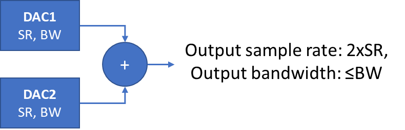
Multiplexing two DACs. SR refers to sample rate, BW refers to bandwidth. Source: Keysight.
“There are two 128GSps 8-bit silicon germanium DACs that are time-interleaved to get a higher speed signal per dimension,” says Pittalá. If the two DACs are shifted in time and added together, the result is a higher sampling rate overall. However, Pittalá points out that while the sample rate is effectively doubled, the overall bandwidth is defined by the individual DACs (see diagram above).
Pittalá also mentions another technique, based on active clocking, that does increase the bandwidth of the system. The multiplexer is clocked and acts like a fast switch between the two DAC channels. “In principle, you can double the bandwidth, ” he says. (See diagram below.)

The Keysight’s M8199B’s improved performance, combined with advances in components such as NTT’s 130GHz indium phosphide amplifier, resulted in over 2Tbps transmission, as detailed in the ECOC 2022 paper. As the baud rate was increased, the modulation scheme used and the net bit rate decreased. (Shown by the red dots on the chart).
In parallel, Keysight worked with Nokia, which used a thin-film lithium niobate modulator for their set-up, a different modulator to NTT’s. The test equipment directly drove the thin-film modulator; no external modulator driver was needed. The system was operated as high as 260GBd, achieving a net bit rate of 800Gbps.
Pittalà notes that while the NTT system differs from Nokia’s, Nokia’s two red points on the extreme right of the chart continue the trajectory of NTT’s six red points as the baud rate increases.
OFC’23 O-band record
The post-deadline papers at the OFC 2023 conference earlier this year did not improve the transmission performances of the ECOC papers.
A post-deadline paper published at OFC 2023 showed a record of coherent transmission in the O-Band. Working with Keysight, McGill University showed 1.6Tbps coherent transmission over 10km using a thin-film lithium niobate modulator. The system operated at 167GBd, used a 64-QAM modulation scheme, and used the Keysight M8199B.
Pittalà expects that at ECOC 2023, to be held in Glasgow in October, new record-breaking transmissions will be announced.
His chart will need updating.
Further information
Thin-film lithium niobate modulators, click here

The market opportunity for linear drive optics
A key theme at OFC earlier this year that surprised many was linear drive optics. Its attention at the optical communications and networking event was intriguing because linear drive – based on using remote silicon to drive photonics – is not new.
“I spoke to one company that had a [linear drive] demo on the show floor,” says Scott Wilkinson, lead analyst for networking components at Cignal AI. “They had been working on the technology for four years and were taken aback; they weren’t expecting people to come by and ask about it. “
The cause of the buzz? Andy Bechtolsheim, famed investor, co-founder and chief development officer of network switching firm Arista Networks and, before that, a co-founder of Sun Microsystems.
“Andy came out and said this is a big deal, and that got many people talking about it,” says Wilkinson, author of a recent linear drive market research report.
Linear Drive
A data centre’s switch chip links to the platform’s pluggable optics via an electrical link. The switch chip’s serialiser-deserialiser (serdes) circuitry drives the signal across the printed circuit board to the pluggable optical module. A digital signal processor (DSP) chip inside the pluggable module cleans and regenerates the received signal before sending it on optically.
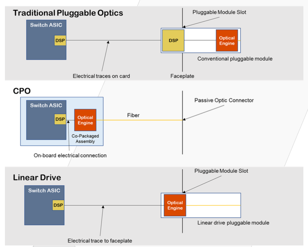
With linear drive optics, the switch ASIC’s serdes directly drives the module optics, removing the need for the module’s DSP chip. This cuts the module’s power consumption by half.
The diagram above contrasts linear drive optics compared with traditional pluggables and the emerging technology of co-packaged optics where the optics are adjacent to the switch chip and are packaged together. Linear drive optics can be viewed as a long-distance variant of co-packaged optics that comntinues to advance pluggable modules.
Proponents of linear drive claim that the power savings are a huge deal. “There will probably also be some cost savings, but it is not entirely clear how big they will be,” says Wilkinson. “But the only thing people want to discuss is the power savings.”
Misgivings
If linear drive’s main benefit is reducing power consumption, the technology’s sceptics counter with several technical and business issues.
One shortfall is that a module’s electrical and optical lanes must match in number and hence data rate. If there is a mismatch, the signal speeds must be translated between the electrical and optical lane rates, known as gearboxing. This task requires a DSP. Linear drive optics is thus confined to 800-gigabit optical modules: 800GBASE-DR8 and 800-gigabit 2xFR4. “There are people who think that at least 800 Gig – eight lanes in and eight lanes out – will continue to exist for a long time,” says Wilkinson.
Another question mark concerns the use of optics for artificial intelligence workloads. Adopters of AI will be early users of 200 gigabit-per-lane optics, requiring a gearbox-performing DSP.
Moreover, the advent of 200-gigabit electrical lanes will challenge serdes developers and, hence, linear drive designs. “It will be a technical challenge, the distances will be shorter, and some think it may never work,” says Wilkinson. “No matter how good the serdes is, it will not be easy.”
Co-packaged optics will also hit its stride once 200-gigabit serdes-based switch chips become available.
Another argument is that there are many ways to save power in the data centre; if linear drive introduces complications, why make it a priority?
Linear drive optics requires the switch chip vendors to develop high-quality serdes. Wilkinson says the leading switch vendors remain agnostic to linear drive, which is not a ringing endorsement. And while hyperscalers are investing time and resources into linear-drive technology, none have endorsed the technology such that they can withdraw at any stage without penalty.
“There is one story for linear drive and many stories against it,” admits Wilkinson. “When you compile them, it’s a pretty big story.”
Market opportunity
Cignal AI believes linear-drive optics will prove a niche market, with 800-gigabit linear-drive modules capturing 10 per cent of overall 800-gigabit pluggable shipments in 2027.
Wilkinson says the most promising example of the technology is active optical cables, where the modules and cables are a closed design. And while many companies are invested in the technology, and it will be successful, the opportunity will not be as significant as the proponents hope.

Agent of change

Dave Welch on how entrepreneurial problem-solving skills can tackle some of society’s biggest challenges
Dave Welch is best known for being the founder and chief innovation officer at Infinera, the optical equipment specialist. But he has a history of involvement in social causes.
In 2012, Welch went to court to fight for the educational rights of children in schools in California, a story covered by newspapers in the US and abroad and featured on the front cover of Time magazine.
“Ultimately, we lost,” says Welch. “But the facts of these [school] practices and their link to a poor educational outcome were confirmed and never disputed.”
Welch recently co-founded NosTerra Ventures, a non-profit organisation tackling challenging social issues. These Grand Challenges, as NosTerra calls them, cover housing, energy and environment, access to healthcare, public education, democracy, and information security, issues more suited to a presidential debate.
“NosTerra aims to identify key societal issues to contribute to, identify differentiated strategies and appropriate entrepreneurs, and help get those launched,” explains Welch. Nosterra has added partners, equivalent to a board of directors, to guide the organisation and ensure its strategies make sense. “We are not a Bill Gates or a Michael Bloomberg, but the object, frankly, is to make an organisation that can have the same influence on how we address these problems,” says Welch.
Welch says his involvement stems from being gifted with various opportunities, creating a responsibility to the greater society. Moreover, these issues define the quality of a society, so it is crucial to address them. “It’s also personally very rewarding to figure out what you can do to help,” says Welch.
Strategy for change
NosTerra works to identify what it must do to contribute to a solution and do it in a differentiated fashion, to make a structural change that improves things over time.
Welch returns to the example of public education and establishing the right to a quality education. “That’s a doable task, and trust me, we will reach out to the Bloombergs and the Gates to ask them for their help,” says Welch.
Energy and the environment is another example. Welch says there is much debate about the topic, which is only right given its impact. But less is discussed about the future direction of energy.
Welch sits on the Natural Resources Defense Council board, an important non-profit organisation, and is involved in setting strategies. He believes NosTerra can pursue various activities, including investing in technologies or creating the opportunity for its partners to invest directly. “In this case, the vehicles of change are that we absolutely need new technologies,” he says, citing the extreme example of fusion to shorter-term battery technologies.
NosTerra also believes it can use politics and influence what Welch calls factual prioritisation Developing solutions to significant problems by 2035 results in a markedly different approach to a 2060 timeframe. “If I’m a government or organisation, where do I want to spend my next pile of money?” says Welch. “What is shocking is that there isn’t a go-to validated model to run such scenarios on.”
Some organisations, such as the US Department of Energy, do have detailed models, but there is no open-source trusted model to see what impact short-term and longer-term investments will have. NosTerra is looking to address this with an open-source energy model so that if the Government is willing to invest $100 billion, it can identify what will give it the best return.
“I applaud the financial attack on the system to convert our energy sources, but I’m also a little appalled at the prioritisation of some of where we spend our money,” says Welch. “We can do some things to help there.”
NosTerra is busy creating a community around these areas to develop solutions to get ‘some of these things done’. Any NosTerra success will not be evident in one or two years but more likely five or ten years.
Welch stresses such ventures is not new to Silicon Valley. “David Packard and Bill Hewlett, those guys not only ran an incredible company [Hewlett-Packard or HP], but they were plugged into their community and sat on school boards,” he says. “I still find Silicon Valley is made up of people that care and work with the community.”
Welch is still fully involved at Infinera. “My added value [at Infinera] is the 40 years of watching telecom technologies develop and watching markets change,” he says. He provides creative thought, a perspective on technologies and why customers and markets will adopt specific directions. He also helps with prioritising what technologies Infinera should develop that will make a difference.
“I love that area,” he says.

The long arm of PCI Express
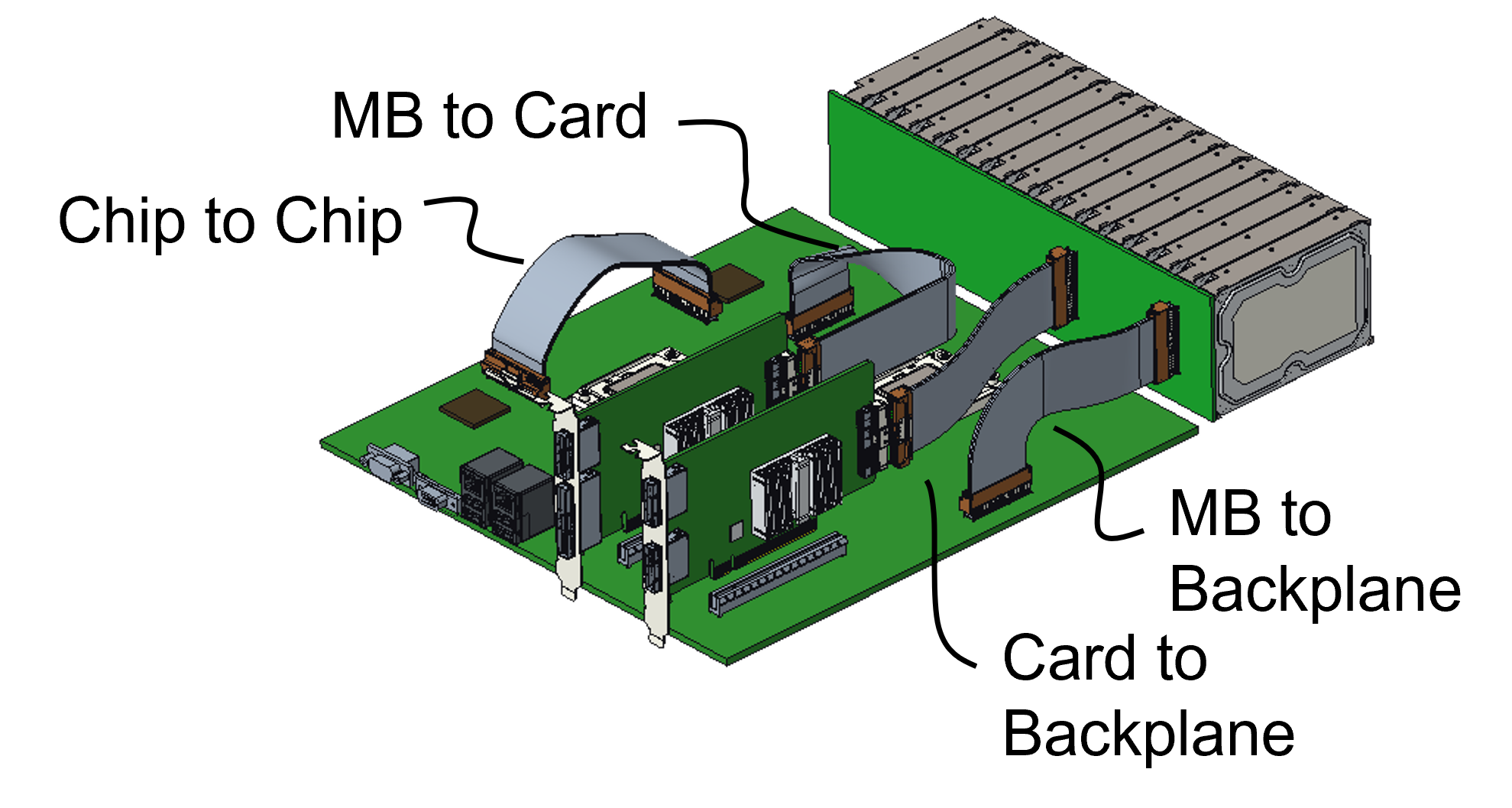
- Optical is being added as a second physical medium to the PCI Express (PCIe) data transfer protocol.
- PCI Express is an electrical standard, but now the Peripheral Component Interconnect Special Interest Group (PCI-SIG) has created a working group to standardise PCIe’s delivery optically.
- PCI-SIG is already developing copper cabling specifications for the PCI Express 5.0 and 6.0 standards.
Since each generation of PCIe doubles the data transfer rate, PCI-SIG member companies want copper cabling to help with the design of high-speed PCIe interconnects on a printed circuit board (PCB), between PCBs, and between racks (see diagram).
“We’ve seen a lot of interest over recent months for an optical cable that will support PCI Express,” says Al Yanes, PCI-SIG president and chairperson.
He cites the trends of the decreasing cost and size of optics and how silicon photonics enables the adding of optics alongside ASICs.
“We have formed a workgroup to deliver an optical cable,” says Yanes. “There are many applications, but one is a longer-distance reach for PCI Express.”
“It is a void in the market [the lack of optical support for PCIe], and it needs to be filled,” says Bill Koss, CEO of Drut Technologies. “These efforts tend to take longer than estimated, so better to start sooner.”
Drut has developed a PCIe over photonics solution as part of its photonic direct connect fabric for the data centre.
The data centre is going photonic, says Koss, so there is a need for such working standards as photonics get closer to processors.
The PCIe protocol
PCIe is used widely across many industries.
In the data centre, PCIe is used by general-purpose microprocessors and accelerator chips, such as FPGAs, graphics processing units and AI hardware, to connect to storage and network interface cards.
The PCIe bus uses point-to-point communications based on a simple duplex scheme – serial transmissions in both directions which is referred to as a lane.
The bus can be bundled in various lane configurations – x1, x2, x4, x8, x12, x16 and x32 – with x4, x8 and x16 the configurations most used.
The first two PCIe versions, 1.0 and 2.0, delivered 2.5 and 5 giga transfers-per-second (GT/s) per lane per direction, respectively.
A transfer refers to an encoded bit. The first two PCIe versions use an 8b/10b encoding scheme such that for every ten-bit payload sent, 8 bits are data. This is why the data transfer rates per lane per direction are 2Gbps and 4Gbps (250 and 500 gigabytes per second), respectively.
With PCIe 3.0, the decision was made to increase the transfer rate to 8GT/s per lane, which assumed that no equalisation would be needed to counter inter-symbol interference at that speed. However, equalisation was required, which explains why PCIe 3.0 adopted 8GT/s and not 10GT/s.
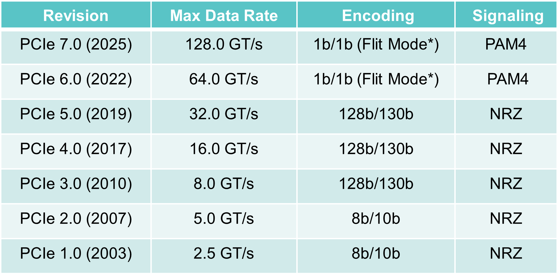
Another PCIe 3.0 decision was to move to a 128b/130b scheme to reduce the encoding overhead from 20 per cent to over 1 per cent. Now the transfer and bit rates are almost equal from the PCIe 3.0 standard onwards.
PCIe 4.0 doubles the transfer rate from 8GT/s to 16GT/s, while PCIe 5.0 is 32GT/s per lane per direction.
Since then, PCIe 6.0 has been specified, supporting 64GT/s per lane per direction. PCIe 6.0 is the first standard for 4-level pulse amplitude modulation (PAM4) signalling.
Now the PCIe 7.0 specification work is at version 0.3. PCIe 7.0 uses PAM-4 to deliver 128GT/s per lane per direction. The standard is expected to be completed in 2025, with industry adoption in 2027.
Optical cabling for PCIe
The PCI Express 5.0 and 6.0 copper cabling specifications are expected by the year-end. The expected distance using copper cabling and retimers is 5-6m.
The reach of an optical PCIe standard will ‘go a lot further’ than that, but how far is to be determined.
Yanes says optical cables for PCIe will also save space: “An optical cable is not as bulky nor as thick as a copper cable.”
Whether the optical specification work will support all versions of PCIe is to be determined.
“There’s some interest to support them all; the copper solution supports all the negotiations,” says Yanes. “It’s something that needs to be discussed, but, for sure, it will be the higher speeds.”
The working group will decide what optical options to specify. “We know that there are some basic things that we need to do to PCI Express technology to make it support optics,” says Yanes.
The working group aims to make the specification work generic enough that it is ‘optical friendly’.
“There are many optical techniques in the industry, and there is discussion as to which of these optical techniques is going to be the winner in terms of usage,” says Yanes. “We want our changes to make PCI Express independent of that discussion.”
The organisation will make the required changes to the base specification of PCIe to suit optical transmission while identifying which optical solutions to address and build.
PCI-SIG will use the same Flit Mode and the same link training, for example, while the potential specification enhancements include coordinating speed transitions to match the optics, making side-band signals in-band, and making the specification more power-efficient given the extended reach.
Pluggable optical modules, active optical cables, on-board optics, co-packaged optics and optical input-output are all optical solutions being considered.
An optical solution for PCIe will also benefit technologies such as Compute Express Link (CXL) and the Non-Volatile Memory Express (NVMe) protocols implemented over PCIe. CXL, as it is adopted more broadly, will likely drive new uses that will need such technology.
The PCIe optical working group will complete the specifications in 12-18 months. Yanes says a quicker working solution may be offered before then.