
Marvell’s CTO: peering into the future is getting harder
CTO interviews part 4: Noam Mizrahi
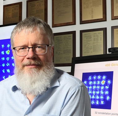
In a wide-ranging interview, Noam Mizrahi (pictured), executive vice president and corporate chief technology officer (CTO) at Marvell, discusses the many technologies needed to succeed in the data centre. He also discusses a CTO’s role and the importance of his focussed thinking ritual.
Noam Mizrahi has found his calling.
“I’m inspired by technology,” he says. “Every time I see an elegant technical solution – and it can be very simple – it makes me smile.”
Marvell hosts an innovation contest, and at one event, Mizrahi mentioned this to participants. “So they issued stickers saying, ‘I made Noam smile’,” he says.
Marvell’s broad portfolio of products spans high-end processors, automotive Ethernet, storage, and optical modules.
“This technology richness means that every day I come to work, I feel I learn something new,” he says.
Chip design
The interview with Mizrahi occurred before the passing away on March 24th of Gordon Moore, aged 94, who co-founded Intel.
In his article published in Electronics in 1965, Moore observed how chip transistor count doubled roughly yearly, what became known as Moore’s law.
The law has driven the semiconductor industry for decades and, like all exponential trends, is reaching its limit.
Since Marvell’s business is infrastructure ICs, it is experiencing the law’s demise first hand.
While the core definition of Moore’s law is ending, technology and process advancement are still enabling the cramming of more transistors on a die, says Mizrahi. However, greater processing performance and lower power consumption are occurring at a different pace and cost structure.
It is now very costly to make chips using the latest 5nm and 3nm CMOS process nodes.
The cost is not just the chip mask (reticle) but also such aspects as intellectual property (IP), architecture, design verification, electronics design automation (EDA) tools, and design validation.
Getting to the first product using 5nm CMOS can cost as high as $450 million, while for 3nm, the estimate is $600 million.
Also, development flow takes longer due to the complexity involved and will cause a redefinition of what is meant by a ‘current generation’ of a chip, says Mizrahi.
Design reuse is also increasingly required; not just reusing IP but the validation process in order to speed up a chip’s introduction.
In turn, designers must be innovative since processing performance and lower power consumption are harder to achieve.
Areas include package design optimisation, chip input-output (I/O), and the software to claw back processing performance that previously came from using the latest CMOS process.
IC designers will also be forced to choose which chips to make using the latest CMOS process node.
Overall, fewer chip companies will be able to afford chips made in leading CMOS processes, and fewer companies will buy such ICs, says Mizrahi.
Rise of chiplets
Chiplets will also play a role in a post-Moore’s law world.
“Chiplets are currently a very hot topic,” says Mizrahi.

A chiplet is a die implementing a functional block. The chiplet is added alongside a central die for a system-on-chip (SoC) design. Using chiplets, designs can exceed the theoretical limit of the mask size used to make a chip.
Marvell has long been a chiplet pioneer, says Mizrahi. “Today, it all seems reasonable, but when we did all that, it was not so obvious.” Marvell makes one chip that has 17 dies in a package.
Chiplets are particularly suited for artificial intelligence (AI) ASICs, what Mizrahi describes as ‘monsters of chips’.
Chiplets enable designers to control yield, which is essential when each 3nm CMOS chip lost to a defect is so costly.
Using chiplets, a design can be made using a mix of CMOS process nodes, saving power and speeding up a chip’s release.
Mizrahi applauds the work of the Universal Chiplet Interconnect Express (UCIe) organisation, creating chiplet standards.
But the chiplets’ first use will be as internally-designed dies for a company’s product, he says. Chip designers buying best-in-class chiplets from third parties remains some way off.
A CTO’s role
Mizrahi’s role is to peer into the future to identify the direction technologies will take and their impact on Marvell’s markets and customers.
He says a company-level longer-term technological strategy that combines the strengths of Marvell’s product lines is needed to secure the company’s technical lead.
“That is my job, and I love it,” he says.
It’s also challenging; predicting the future is hard, especially when the marketplace is dynamic and constantly changing. Technology is also very costly and time-consuming to develop.
“So, making the right decision as to what technology we need to invest in for the future, that is tough,” says Mizrahi.
Rapidly changing market dynamics are also challenging Marvell’s customers, who don’t always know what they need to do.
“Creating this clarity with them is challenging but also a great opportunity if done correctly,” says Mizrahi. “That is what keeps me motivated.”
Job impact
How does Mizrahi, Marvell’s CTO since 2020, assess his impact?
The question stems from a comment by Coherent’s Dr Julie Eng that assessing a CTO’s impact is more complicated than, say, a product line manager’s. On becoming CTO, Eng discussed with Coherent’s CEO how best to use her time to benefit the company. She also called other CTOs about the role and what works for them.
“I would say that my goals are tangible and clear, but the environment and the topics that I deal with are far less tangible and clear,” says Mizrahi.
He is required to identify technology trends and determine which ones need to be ’intercepted’. “What do we need to do to get there and ensure that we have the right technologies in place,” he says.
But how technologies play out is hard to determine and becoming harder given the longer development cycles.
“It’s critical to identify these technologies and their impact ahead of time to give yourself enough time to prepare for what must be done, so you can start the development in time for when the wave hits.”
Marvell’s strategy
Marvell’s company focus is infrastructure IC.
“We deal with the network, connectivity, storage, security, all the infrastructure around the processor,” says Mizrahi.
Marvell has been acquiring companies to bolster its technology portfolio and system expertise. The acquisitions include Cavium, Inphi, and Innovium. Last year, Marvell also bought CXL specialist Tanzanite Silicon Solutions.
“It’s going to be very important that you possess all the components in the infrastructure because, otherwise, it is tough to design a solution that brings value,” says Mizrahi.
Being able to combine all the pieces helps differentiate a company.
“I’m not sure there are many other companies that possess all the components needed to make effective infrastructure,” he says.
Disaggregation
Mizrahi gave a talk at Marvell’s Industry Analyst Day last December entitled Disaggregation using Optics.
During the talk, he described how data centres have been flexible enough to absorb new use cases and applications in the past, but now this is changing.
“AI training clusters are going to require a different type of data centre,” says Mizrahi. “It is more like a supercomputer, not the same traditional server architecture we see today.”
His analyst day talk also highlighted the need to disaggregate systems to meet the pace of scaling required and remove dependencies between components so they can be disaggregated and scaled independently.
Compute Express Link (CXL) and memory is one such component disaggregation example.
The CXL protocol optimises several memory parameters in computing systems, namely latency, bandwidth, and memory semantics. Memory semantics is about overseeing correct access by several devices using a shared memory.
CXL enables the disaggregation of memory currently bound to a host processor, thereby not only optimising the performance metrics but reducing overall cost.
Mizrahi cites the issue of poor memory usage in data centres. Microsoft Azure issued research that showed half of its virtual machines never touch half the memory.
“This means that memory is stranded when virtual machines are rented and are unavailable to other users,” says Mizrahi. “And memory is one of the largest spends in data centres.”
CXL enables memory pooling. From this pool, memory is assigned to an application in real time and released when workload execution is completed.
Pooled memory promises to save hyperscalers hundreds of millions of dollars.
“Of course, it’s not easy to do, and it will take time, but that’s just one motivation for doing things [using CXL].”
His analyst talk also stated how optics is the one media that addresses all the disaggregation issues: bandwidth, power, density, and the need for larger clusters.
“We’re going to see an all-optical type of connectivity if you look far enough into the future,” he says. “Of course, not today and not tomorrow.”
Mizrahi’s talk also suggested that AI will need even larger scale computing than supercomputers.
He cites Tesla’s supercomputer used to train its autonomous vehicle neural network.
“If you look at what it is composed of, it is a supercomputer,” says Mizrahi. “Some say it’s one of the top five or top 10 supercomputers, and its only purpose is to train autonomous vehicle neural networks.”
Last year, Meta also announced a supercomputer for training purposes.
Such AI training systems are the tip of the iceberg, he says.
“Ask yourself, what is a unit for a training cluster,“ says Mizrahi. “Is it eight GPUs (graphics processing units), 256 GPUs, 4k TPUs (tensor processing units), or maybe it is an entire data centre in one cluster?”
That is where it is all going, he says.
Pluggable modules and co-packaged optics
Co-packaged optics continues to evolve, but so are standard pluggable modules.
There is a good reason why pluggable optics remain in favour, and that will continue, says Mizrahi. But at some point, designers won’t have a choice, and co-packaged optics will be needed. That, however, is some way off.
In time, both these technologies will be used in the data centre.
Co-packaged optics is focussed on high-capacity networking switches. “And we are right in the middle of this and developing into it,” says Mizrahi.
Another place where co-packaged optics will be used, potentially even sooner, is for AI clusters.
Such co-packaged optics will connect switches to compose AI clusters, and, longer term, the GPUs will use optical I/O as their primary interface.
Such optical I/O helps meet bandwidth, power reduction, and power density requirements.
“Let’s say you want to build a cluster of GPUs, the larger the cluster, the better, but these are so power-hungry. If you do it with electrical connectivity, you must maintain proximity to achieve high speeds,” says Mizrahi. “But that, of course, limits your ability to put more GPUs into a cluster because of power density limitations.”
Using optical I/O, however, somewhat eases the density requirement, enabling more GPUs in a cluster.
But there are issues. What happens if something fails?
Today, with pluggables, one link is affected, but with co-packaged optics, it is less simple. “Also how do you scale production of these things to the scale of a data centre?” says Mizrahi.
These questions will ensure the coexistence of these different solutions, he says.
But AI is driving the need for the newer technology. Mizrahi cites how, in data centres, high-end switches have a capacity of 25 terabits while servers use a 50-gigabit interface. “That means, if for simplicity we ignore topologies and redundancies, you can connect 500 servers to that switch,” he says.
GPUs today have a 3.6 terabit-per-second full duplex I/O connectivity to talk to their peer GPUs.
“It only takes seven GPUs to saturate that very same [25.6-terabit capacity] switch,” he says. “The bandwidth requirement, it just explodes, and it’s going to be very hard to keep doing that electrically.”
This is why co-packaged optics will be needed.
Typical workday
Mizrahi is based in Israel, whereas Marvell’s headquarters is in Santa Clara, California.
“It [Israel] is the centre of my life and where my family is,” says Mizrahi. “I travel a lot, to the point where I think my biological clock is somewhere over the ocean.”
His day spreads across many time zones. Early morning calls are to the Far East before he turns to local issues. Then, his afternoon coincides with morning US Eastern time, while his evening aligns with morning US Western time.
That said, Marvell’s CEO repeatedly emphasises his desire for all employees to balance work and family.
“He encourages and insists to see that happen, which helps me keep a balance,” says Mizrahi.
Prime focus time
Mizrahi loves sports and is a keen runner.
He ensures he does not miss his seven or eight-mile daily run, even on days when he has a long flight.
“Every morning, it is my alone time,” he says. “It’s when I let my brain work, and it is my prime focus time.”
He is also a family man and has three children. He is keen to spend as much time as possible with his wife and kids.
“It’s not going to be long before they [the children] start their journey away from home, so I try to cherish every minute I have with them,“ he says.
He reads a lot, including technical material. “I told you, I’m inspired by technology.”

He cites two recently read books.
One, in Hebrew, is called Red Skies by Daniel Shinar.
“It talks about a friendship between two young guys from two sides of the fence,” he says. A friendship that proves impossible due to the reality of the situation.
The second book, one he found fascinating and meaningful, was part of a training course given at Marvell, called The Leadership Challenge by James Kouzes and Barry Posner.
“It gives you practices that the authors see as key for exemplary leadership, and it gave me so many things to think about,” he says. “To recognise things in my behaviour or other people, I view as leaders.”
How DSP smarts continue to improve optical transport
- Kim Roberts explains the signal processing techniques Ciena is using for its WaveLogic 6 coherent DSP.
- Roberts explains how the techniques squeeze, on average, a 15 per cent improvement in spectral efficiency.
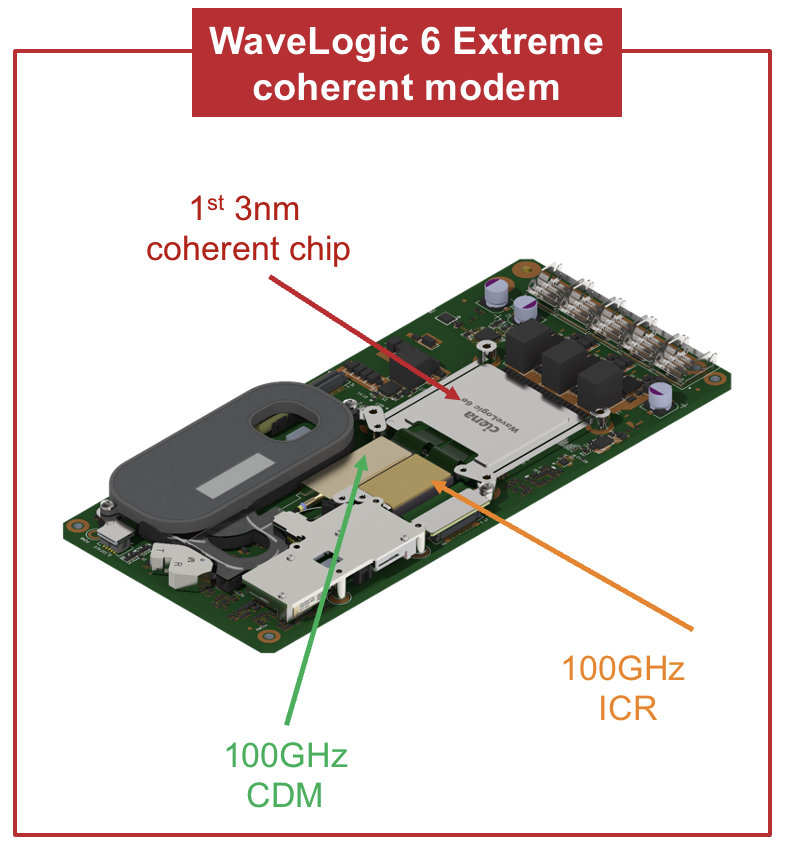
- The WaveLogic 6 Extreme chip can execute 1,600 trillion (1.6 x 10¹⁵) operations per second and uses the equivalent of 4km of on-chip copper interconnect.
Part 2: WaveLogic 6’s digital signal processing toolkit
Bumping into Kim Roberts on the way to the conference centre at OFC, held in San Diego in March, I told him how, on the Ciena briefing about its latest WaveLogic 6 coherent digital signal processor (DSP), there had been insufficient time to dive deeply into the signal processing techniques used.
“What are you doing now?” said Roberts.
“I’m off to the plenary session to catch the keynotes.”
Chatting some more, I realised I was turning down a golden opportunity to sit down with a leading DSP and coherent modem architect.
“Is that offer still open?” I asked.
He nodded.
We grabbed a table at a nearby cafe and started what would prove to be an hour-long conversation.
High-end coherent DSPs
Many leading coherent modem vendors unveiled their latest designs in the run-up to the OFC show. It is rare for so many announcements to be aligned, providing a valuable glimpse of the state of high-performance optical transport.
Nokia announced its PSE-6s, which has a symbol rate of up to 130 gigabaud (GBd) and supports 1.2 terabit wavelengths. Infinera announced its 1.2-terabit ICE-7, which has a baud rate of up to 148GBd, while Fujitsu detailed it is using its 135GBd 1.2-terabit wavelength coherent DSP for its 1FINITY Ultra optical platform.
Meanwhile, Acacia, a Cisco company, revealed its 140GBd Jannu 1.2-terabit DSP has been shipping since late 2022. Acacia announced the Jannu DSP in March 2022.
All these coherent DSPs are implemented using 5nm CMOS and are shipping or about to.
And Ciena became the first company to detail a coherent DSP fabricated using a 3nm CMOS process. The WaveLogic 6 Extreme supports 1.6-terabit wavelengths and has a symbol rate of up to 200GBd.
Ciena’s WaveLogic 6 Extreme improves spectral efficiency by, on average, 15 per cent. WaveLogic 6 Extreme-based coherent modems will be available from the first half of 2024.
Customer considerations
Kim Roberts begins by discussing what customers want.
“With terrestrial systems, it is cost-per-bit [that matters], and if you’re not going very far, it is cost-per-modem,” says Roberts.
For the shortest reaches (tens of km), 100 gigabit may be enough while 200 gigabit or more is overkill. Here, a coherent pluggable module does the job.
“What matters is the cost per modem to get the flexibility of coherent connectivity so that you can plug it in and it works,” says Roberts.
With medium and long-haul terrestrial routes, cost-per-bit and heat-per-bit are the vital issues. With heat, area and volume of the coherent design are important. “I need volume to get the heat out of the chip on the card and into the air,” says Roberts.
Another use case is where spectral efficiency is key, for networks where fibre is scarce. An operator could be leasing dark fibre, or it could be a submarine network.
Ciena’s WaveLogic 6 Extreme’s 15 per cent improvement in spectral efficiency improves capacity over the same link. “Equivalently, you can go a dB (decibel) further or have a dB more signal margin,” says Roberts.
A common refrain heard is that spectral efficiency is no longer improving due to the Shannon limit being approached. Shannon’s limit is being approached because of the considerable progress already made by the industry in coherent optics.
“There is no 6dB to be had like in the old days,” says Roberts. “WaveLogic 3 was 2.5dB better than WaveLogic 2, but those multiple dBs are no longer there.”
The returns are diminishing, but striving for improvements remains worthwhile. “If you’re an operator that cares about spectral efficiency, that’s important,” he says.
Nonlinearity mitigation
Roberts returns to the issue of Shannon’s limit, based on the work of famed mathematician and information theorist, Claude Shannon.
“Shannon defines a theoretical limit for the capacity of a channel having linear propagation with additive Gaussian noise,” says Roberts.
This defines a strict mathematical limit, and it is pointless to go beyond that; he says: “In terms of linear performance, modems are getting close to the limit, within a couple of dB.”
Shannon’s limit doesn’t wholly define fibre since the channel is nonlinear.
Roberts says there is a whole research area addressing the bounds given such nonlinearities.
“We’re a long way from those theoretical nonlinear limits, but what matters is what’s the practical limit, and it’s getting hard,” he says
Increasing transmit power improves the optical signal-to-noise ratio (OSNR) and strengthens nonlinearities. Indeed, the nonlinearities grow faster with increased transmit power until, eventually, they dominate.
Because tackling nonlinearities is so complicated, Ciena’s approach is to approximate the problem as a linear Gaussian noise channel and do everything possible to mitigate the effects of nonlinearity rather than embrace it.
This is done by compensating at the transmitter the nonlinearities expected to happen along the fibre. The receiver performs measurements on a second-by-second basis and sends the results back. These are used as estimates of the anticipated nonlinearity about to be encountered and subtracted from the symbols to be sent.
Even though the exact nonlinearity is unknown, this is still a valid approximation. “It gives a quarter to one dB of performance improvement,” says Roberts
Edgeless clock recovery
Robert explains other clever signal processing techniques that buy a 6 per cent spectral efficiency improvement.
With wavelength division multiplexing (WDM), the laser-generated signals are placed next to each other across the fibre’s spectrum.
For WaveLogic 6, when running at its maximum symbol rate of 200 gigabaud, the spectrum occupies a 200GHz-wide channel.
Usually, the signal in the frequency domain is not perfectly square-shaped; the signal rolls off in the frequency domain so that in the time domain there is no inter-symbol interference. “But [as a result] you’re wasting spectrum; you are not fully using that spectrum,” says Roberts.
With WaveLogic 6, Ciena has created an idealised flat-topped, vertically edged signal spectra allowing the signals to be crammed side by side thereby making best use of the fibre’s spectrum (see diagram).
The challenge is that the clocking information used for data recovery at the receiver resided in this roll-off region. Now, that is no longer there so Cienahas developed another method to recover clock information.
A second challenge with signal recovery is that the transmit laser and the receive laser are not rigidly fixed in frequency. Being so close together, care is needed to recover only the wavelength – signal – of interest.
Yet another complication is how a rectangle in the frequency domain causes the signal in the time domain to ‘ring’ and go on forever.
“There are several signal processing methods that we had to develop to make this possible,” says Roberts.
Frequency-division multiplexing
Ciena also uses frequency division multiplexing (FDM), a technique it first introduced with the WaveLogic 5 Extreme.
The difference between WDM and FDM, explains Roberts, is that WDM uses different lasers to generate the wavelengths while FDM is generated by applying digital techniques to the same laser. “You are digitally combining different streams,” he says.
This is useful because it turns out that each fibre route has an optimum baud rate because of nonlinearities.
“If I’m using the full symbol rate of 200GBd, I can divide that into parallel streams, which behave as if they were independent circuits as far as nonlinearity is concerned,” says Roberts. “The optimum number of FDM in your spectrum is proportional to the square root of the total amount of dispersion, so high dispersion, more FDMs, low dispersion, just one.”
Ciena first added the option of four FDM with the WaveLogic 5. Now, WaveLogic 6 implements 1,2,4, and 8 FDM channels.

“For short distances, you want to go one signal at 200 gigabaud, or smaller if you’re reducing baud rate, but if you’re going very long distances, lots of dispersion, you go at eight parallel streams being sent at 25 gigabaud each,” he says.
But introducing FDM causes notches in the near-idealised rectangular spectrum mentioned earlier. Ciena has had to tackle that too.
“If you measure the spectrum, it’s completely flat, there are no notches between the FDMs, there is no wasted spectrum,” says Roberts.
Multi-dimensional coding
Multi-dimensional coding is a further technique used by Ciena to improve optical transmission, especially in troublesome cables where there are much nonlinearity and noise. It is challenging to get information through.
To understand multi-dimensional constellations, Roberts uses the example of a 16-QAM constellation, which he describes as a two-dimensional (2D) representation in one polarisation.
But if both polarisations of light are considered one signal, it becomes a 4D, 256-point (16×16) symbol. This can be further extended by including the symbols in adjacent time slots to form an 8D representation.
Ciena introduced this technique with its WaveLogic 3 Extreme coherent DSP, which supported the multi-dimension coding scheme 8D-2QAM to improve the reach or capacity of long-reach spans.
Now Ciena has introduced a family of such multi-dimensional schemes with WaveLogic 6 Extreme, executing in regions of very high nonlinearity and noise. These include 4, 8, and 16-dimensional constellations.
An example where the technique is used includes cases where there is twice as much noise as there is signal. “So the signal-to-noise ratio is -3dB,” says Roberts. Yet even here, 100 gigabits can still get through.
WaveLogic 6 Nano
Ciena also announced its 3nm CMOS WaveLogic 6 Nano DSP aimed at pluggable coherent modules. Is the Nano’s role to implement a subset of the signal processing capabilities of the Extreme?
Here, the customer’s requirements are different: heat, space and footprint are the dominant concerns. The Nano has to fit the heat envelope of the different sizes of pluggables, says Roberts. The optical performance is chosen based on fitting that heat requirement.
One of the merits of 3nm FinFET transistor technology is that if you don’t clock a circuit, only 1 per cent of the heat is generated compared to when it’s clocked, notes Roberts: “So, for different features, I can turn off the clock.”
A suitcase still full of tools?
At the time of the WaveLogic 5 launch, Roberts mentioned that there were still many tools left in the suitcase of ideas. Is this still true with the WaveLogic 6?
For Roberts, the question is: will it be economically viable to put in new capabilities based on the heat and performance and in terms of the size, schedule, and the amount of work involved?
Then, with a broad smile, he says: “There is room to occupy us as to how to get the next 10 to 20 per cent of spectral efficiency.”
And with that, we each set off for a day of meetings.
Roberts headed off to his hotel before his 10am meeting. I set off for the OFC exhibition hall and a meeting with the OIF.
As I walked to the convention centre, I kept thinking about the impromptu briefing and how I so nearly passed up on Roberts’ expertise and generosity.

Do optical DACs have a role in future coherent modems?
- A proposed optical digital-to-analogue converter (oDAC) concept offers several system benefits, including better signal performance, higher bit rates and lower power consumption.
- The oDAC design benefits coherent optics but can also be used in direct-detect designs. This article focusses on coherent optics.
- Coherent system vendors are aware of oDAC technology but it is not part of their current roadmaps.
Systems vendors continue to advance the performance of optical transmission systems. But they are the first to admit the task is getting more complex.
Long-distance transmission is challenging due to the channel impairments introduced by the optical fibre, such as noise, chromatic dispersion, and non-linearities.
Coherent modems have become the established technology that use a powerful digital signal processor (DSP) and optics to counter channel impairments.
In recent years the industry has progressed coherent technology to such a degree that it is now difficult to keep improving optical performance.
One critical component of the coherent DSP is the analogue front end: the transmitter’s digital-to-analogue converters (DACs) and the receiver’s analogue-to-digital converters (ADCs).
The DACs take the digital signal input and produce the analogue drive signal for the coherent optics’ Mach-Zehnder modulators. In turm, the DSP’s ADCs sample the signal at the receiver’s optics before recovering the transmitted data payload.
The challenge facing coherent DSP designers is to keep scaling the bandwidth of the DACs and ADCs while maintaining high resolution and high energy efficiency.
This growing challenge has led some researchers to propose alternatives.
One such proposal is an optical digital-to-analogue converter or oDAC.
The status of coherent DSPs
Recent announcements from leading coherent optic vendors, including Cisco’s Acacia, Ciena, Infinera, NEL, and Nokia, show the continual progress in hiking the symbol rate of coherent DSPs.

Vendors want to keep increasing the symbol rate – the frequency of the symbols where each symbol carries one or more bits, depending on the modulation scheme used – since it remains the best way to reduce the cost of sending network traffic.
First-generation coherent systems used a symbol of 32 gigabaud (GBd). Now, Acacia’s currently shipping 5nm CMOS Jannu DSP operates at up to 140GBd. Ciena, meanwhile, has detailed its WaveLogic 6 Extreme, the first coherent DSP implemented in 3nm CMOS that will work at up to 200GBd.
To scale the baud rate, all the sub-systems making up the coherent modem must scale.
The sub-systems include the DSP’s DACs and ADCs, the modulator drivers, and the trans-impedance amplifiers. The coherent optics – the coherent driver modulator (CDM) transmitter and the integrated coherent receiver (ICR) – must also scale.
For a 200GBd symbol rate, the bandwidth of all these components must reach 100GHz.
Looking ahead
The industry consensus is that coherent modems will reach 280-300GBd before the decade’s end. But to do so will require considerable engineering effort.
The industry offers less visibility after 300+GBd.
System vendors say that at some future point, it will not make economic sense to keep increasing the baud rate. It will be too costly to make the coherent modem and reducing the cost-per-bit will stop.
Already each new generation CMOS node is more costly while new materials are needed to scale the optics. Ciena says it is using silicon photonics for the integrated coherent receiver, while indium phosphide is being used for the transmitter’s modulators. Ciena is also looking at thin-film lithium niobate as a modulator technology.
As for DACs and ADCs, circuit designers face considerable challenges in achieving a 100GHz bandwidth.
Moreover, the DACs and ADCs sample faster than the baud rate, typically 1.2x. At OFC, imec, the Belgium technology research centre, outlined its work on 3nm coherent DSPs showing a sample rate of 250 giga-samples/s.

Such huge sampling rates explain the interest in optical DACs which can process a high-baud rate signal to generate, using optical parallelism, an ultra-high bit-rate signal based on either multi-level Pulse Amplitude Modulation (PAM) or Quadradure Amplitude Modulation (QAM) signals.
Two prominent professors promoting an optical DAC design are Ioannis Tomkos of the department of electrical and computer engineering at the University of Patras, Greece, and Moshe Nazarathy at the faculty of electrical engineering at the Technion University, Israel.
Limitations of DACs
Tomkos starts by highlighting the shortcomings of conventional DACs.
DACs not only have to operate sampling rates at least as high as the baud rate but they also have a finite resolution. Typically, 6-8 bits are used for coherent designs.
The effective number of bits (ENOB) available are even lower due to the clock jitter when operating the electrical circuits at such high speeds.
The finite effective number of bits limit the use of higher-order modulation schemes. Today, coherent systems use up to 16-ary quadrature amplitude modulation (16-QAM), except for the highest capacity, shortest-distance links.
A second issue is the non-linear nature of the optical modulator’s transfer function. “It’s a sine non-linearity type of response in Mach-Zehnder modulators due to the nature of interference,” says Tomkos.
This requires operating the modulator over a reduced range, the linear region of its transfer function around its biasing voltage.
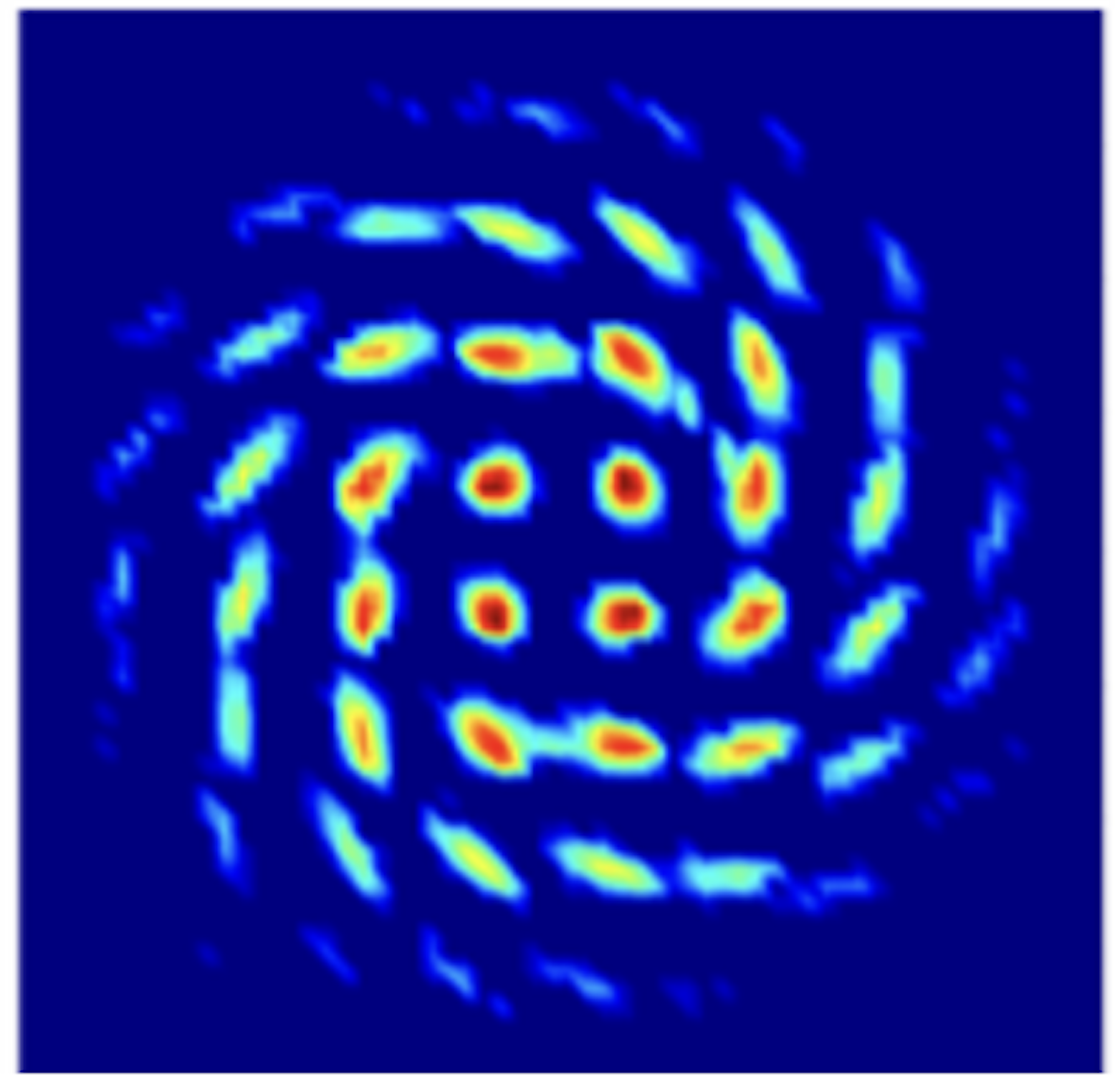
Such curtailing of the driver saves power but results in ‘modulator loss’; the area occupied by the modulator’s constellation points is less than the ideal available (see top left diagram).
“You not driving the modulator to the limit,” says Tomkos. “Modulation loss can be as high as 9-12dB which impacts signal recovery at the receiver.”
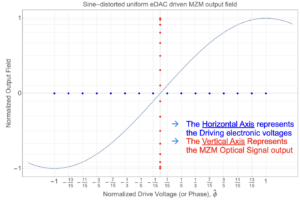
The relation between the driving DAC inputs and the discrete optical outputs is generally nonlinear (see diagram above). This means the constellation points look warped and are not spaced equally apart causing signal distortion.
Such optical distortion can be tackled using various specialised DAC architectures but the cost is either higher power, limited speed or extra modulation loss.
“Ideally, we would like to have equal distances between the symbols so we can robustly separate each symbol from the others since we also have electronic errors coming from the DACs that impact the quality of the symbols and shift them from their optimal points,” says Tomkos.
The impact of modulation loss and optical distortion also worsen when higher modulation schemes above 16-QAM are used.
The oDAC
Mention the term optical DAC, and specific thoughts come to mind. Is the optical signal sampled? Is the DAC electrical in its input and output, but its inner workings are photonic?
The optical DAC, as proposed by Nazarathy and Tomkos, is neither of the above. Moreover, it uses existing driver electronics based on the simplest traditional lowest-order DACs.
Indeed, the oDAC looks similar to a conventional coherent optics transmitter in terms of components, but the differences in operation and achieved performance are significant.
The oDAC can also be implemented in several ways bringing critical benefits for various system requirements.
Architecture
A conventional coherent optical transmitter splits the incoming laser source and feeds the light equally to the in-phase and quadrature Mach-Zehnder modulators (one arm of which includes a 90-degree phase shifter).

The two Mach-Zehnder modulators are driven, as shown. In this example, two drivers implement a bipolar 4-level pulse amplitude modulation (PAM-4) signal such that the coherent transmitter produces a 16-QAM output signal.
The oDAC architecture is subtly different.
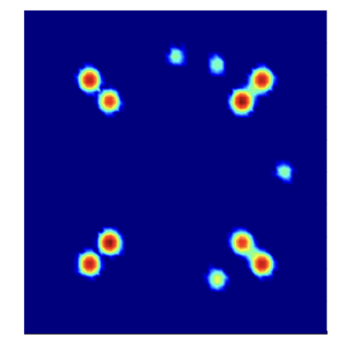
The oDAC’s main two components are a variable splitter and combiner at the input and output and the Mach-Zehnder modulator pair. Here, both modulators are identical; there is no 90o phase shifter but the differential phase is maintained at 0o degrees and the modulators are operated at full-scale resulting in zero modulation loss (see diagram at the article’s start).

Each modulator arm is driven by an electrical PAM-4 signal, and the variable splitter-combiner produces the bipolar PAM-16 optical output.
For 16-PAM, 4/5 of the laser signal is fed to one arm and the remaining 1/5 to the other. The PAM-4 DAC drivers for both Mach-Zehnder modulators are identical.
“In the first case, we had 16 symbols in two dimensions (i.e. QAM16); here we have 16 symbols, but in one dimension (i.e. PAM16), the other dimension is missing due to the absence of the 90-degree phase shifter,” says Tomkos.
According to Tomkos, the sine nonlinearity of the optical modulators here is an advantage. “The generated signal does not suffer from modulation loss and optical distortion due to electronic driver mismatch errors, as the noise coming from the electronic DACs gets squelched,” he says.
Higher-order modulation
As mentioned, the oDACs can be implemented and arranged in several ways.
For example, two oDACs can be used, one orthogonal in phase to the other, in a conventional coherent transmitter structure to generate a higher modulation signal. For example, two optical DAC arms, each 16-PAM, used as I and Q, will produce a 256-QAM signal.
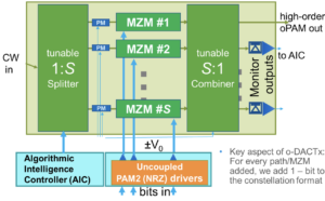
But even more strikingly, more than two parallel modulation paths (by stacking-up more modulators in parallel, see diagram) can be used as an alternative approach to generating higher-order modulation schemes and higher bit rates, and at reduced power consumption per bit.
“The ratio between the bit rate and the baud rate is exactly the number of parallel paths,” says Nazarathy. “Another name for it is spectral efficiency: how many bits each symbol carries.”
The oDAC uses straightforward drivers. The professors say only PAM-2 or PAM-4 drivers are used. This way, power savings are maximised.
“The big picture is that we offload the electronics burden by going parallel optically,” says Nazarathy, adding that what is being traded is electronic DAC complexity and the associated performance limitations of the drivers for optical parallelism of replicated blocks of Mach-Zehnder modulators.
“You don’t want to stack things [photonic componentry] serially as if you keep stacking that way, you incur an optical loss because the loss is compounded,” says Nazarathy. Here, the modulators are stacked in parallel, the preferred integration approach.
Moreover, the more paths used, the higher-order the generated optical constellation is. “Eventually, only PAM-2 (Non-return-to-zero) drivers are used and that’s the minimum power consumption you can get,” says Tomkos.
“So we have parallelism (at the same laser power) that generates for the same baud rate, double or triple the bit rate [depending on whether 2 or 3 paths are used],” says Nazarathy. And the resulting constellations are near ideal: there is no modulation loss, nor is there optical distortion.
Nazarathy explains such benefits as the result of a ‘divide-and-conquer’ approach.
“If you keep the modulation paths simple, you have more freedom to optimise the drive point of the modulators,” he says. “The modulators benefit you more because they are more simply driven.” Then, by adding more modulator paths, the system performance improves overall.”
He also notes how the optical implementation is robust to imperfections generated by the electronic circuitry.
Optical DAC: A definition
- Two or more optical modulator units and some static or slowly-tuned ‘glue’ optics.
- The electrical drivers feeding the optical modulators are simple for lowest-power, either PAM2 (NRZ) or PAM4 drivers. Electronic DACs generating higher-order PAM are not needed.
- No high-speed power-hungry digital encoder (mapper) is used. The number of Mach-Zehnder modulators is B where the constellation size is C=2B. This is referred to as Direct Digital Drive. This last condition ensures the lowest power consumption.
Status
The oDAC work is currently at the research stage.
The working of the oDAC has been simulated and verified, and several papers have been published. Patents have also been filed.
At the recent OFC event in San Diago in March, Professor Tomkos met with hyperscalers, systems and components vendors to explain the oDAC technology and its benefits.
The two academics are focused on the oDAC in the optical transmitter, but Nazarathy says they also plan to surprise at the optical receiver end.
Tomkos says the optical DAC is an ideal fit for future coherent transmitters that will be used in 6G networks and datacenter networks, which will carry significant amounts of traffic at ultra-high rates.
The oDAC approach also bodes well for the trend of using linear drive optics. Indeed, the implementation of the oDAC hardware is carried out within the framework of a major R&D project called FLEX-SCALE that Tomkos is co-ordinating and is funded under the first phase of the 6G Smart Networks and Services (SNS) Partnership.
Tomkos believes that the first use of the optical DAC may likely be for data centre interconnect, a more mature market where higher-order modulation formats can be used and low-power is at a premium.
The professors are looking for partners and exploring options to commercialise the technology.

Ciena advances coherent technology on multiple fronts
- Ciena has unveiled the industry’s first coherent digital signal processor (DSP) to support 1.6-terabit wavelengths
- Ciena announced two WaveLogic 6 coherent DSPs: Extreme and Nano
- WaveLogic 6 Extreme operates at a symbol rate of up to 200 gigabaud (GBd) while the Nano, aimed at coherent pluggables, has a baud rate from 118-140GBd
Part 1: WaveLogic 6 coherent DSPs
Ciena has leapfrogged the competition by announcing the industry’s first coherent DSP operating at up to 200GBd.
The WaveLogic 6 chips are the first announced coherent DSPs implemented using a 3nm CMOS process.
Ciena’s competitors are – or will soon be – shipping 5nm CMOS coherent DSPs. In contrast, Ciena has chosen to skip 5nm and will ship WaveLogic 6 Extreme coherent modems in the first half of 2024.
Using a leading CMOS process enables the cramming of more digital logic and features in silicon. The DSP also operates a faster analogue front-end, i.e. analogue-to-digital converters (ADC) and digital-to-analogue (DAC) converters.
The WaveLogic 6 matches Ciena’s existing WaveLogic 5 family in having two DSPs: Extreme, for the most demanding optical transmission applications, and Nano for pluggable modules.
WaveLogic 6 Extreme is the first announced DSP that supports a 1.6-terabit wavelength; Acacia’s (Cisco) coherent DSP supports 1.2-terabit wavelengths and other 1.2-terabit wavelength DSPs are emerging.
WaveLogic 6 Nano addresses metro-regional networks and data centre interconnect (up to 120km). Here, cost, size, and power consumption are critical. Ciena will offer the WaveLogic 6 in QSFP-DD and OSFP pluggable form factors.
Class 3.5
Network traffic continues to grow exponentially. Ciena notes that the total capacity of its systems shipped between 2010 and 2021 has grown 150x, measured in petabits per second.
Increasing the symbol rate is the coherent engineers’ preferred approach to reduce the cost per bit of optical transport.
Doubling the baud rate doubles the data sent using the same modulation scheme. Alternatively, the data payload can be sent over longer spans.
However, upping the symbol rates increases the optical wavelength’s channel width. Advanced signal processing is needed to achieve further spectral efficiency gains.
One classification scheme of coherent modem symbol rate defines first-generation coherent systems operating at 30-34GBd as Class 1. Class 2 modems double the rate to 60-68GBd. The OIF’s 400ZR standard operating at 64GBd is a Class 2 coherent modem.
Currently-deployed optical transport systems operating at 90-107GBd reside between Class 2 and Class 3 (120-136GBd). Ciena’s WaveLogic 5 Extreme is one example, with its symbol rate ranging from 95-107GBd. Ciena has shipped over 60,000 WaveLogic 5 Extreme DSPs to over 200 customers.
Acacia’s latest CIM-8 coherent modem, now shipping, operates at 140GBd, making it a Class 3 design. Infinera, NEL, and Nokia announced their Class 3 devices before the OFC 2023 conference and exhibition.
Now Ciena, with its 200GBd WaveLogic 6 Extreme, sits alone between Class 3 and Class 4 (240-272GBd).
WaveLogic 6 Extreme
Ciena has extended the performance of all the components of the Extreme-based coherent modem to work at 200GBd.
These components include the DSP’s analogue front-end: the ADCs and DACs, the coherent optics and the modulator drivers and TIAs. All must operate with a 100GHz bandwidth.
To operate at 200GBd, the ADCs and DACs must sample over 200 giga-samples a second. This is pushing ADC and DAC design to the limit.
The coherent modem’s optics and associated electronics must also have a 100GHz operating bandwidth. Ciena developed the optics in-house and is also working with partners to bring the coherent optics to market with a 100GHz bandwidth.
Ciena uses silicon photonics for the Extreme’s integrated coherent receiver (ICR) optics. For the coherent driver modulator (CDM) transmitter, Ciena is using indium phosphide and is also evaluating other technology such as thin-film lithium niobate.
“There are multiple options that are available and being looked at,” says Helen Xenos, senior director of portfolio marketing at Ciena.
Much innovation has been required to achieve the fidelity with 100GHz electro-optics and get the signalling right between the transmitter-receiver and the ASIC, says Xenos.
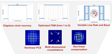
Ciena introduced frequency division multiplexing (FDM) sub-carriers with the WaveLogic 5 Extreme, a technique to help tackle dispersion. With the introduction of edgeless clock recovery, Ciena has created a near-ideal rectangular spectrum with sharp edges.
“First, inside this signal, there are FDM sub-carriers, but you don’t see them because they are right next to each other,” says Xenos. “Getting rid of this dead space between carriers enables more throughput.”
Making the signal’s edges sharper means that wavelengths are packed more tightly, better using precious fibre spectrum. Edgeless clock recovery alone improves spectral efficiency by between 10-13 per cent, says Xenos.
Moving to 3nm allows additional signal processing. As an example, Ciena’s WaveLogic 6 Extreme DSP can select between 1, 2, 4 and 8 sub-carriers based on the dispersion on the link. WaveLogic 5 Extreme supports 4 sub-carrier FDM only.
The baud rate is also adjustable from 67-200GBd, while for the line rate, the WaveLogic 6 supports 200-gigabit to 1.6-terabit wavelengths using probabilistic constellation shaping (PCS).
Another signal processing technique used is multi-dimensional constellation shaping. These are specific modulations that are added to support legacy submarine links.
“For compensated submarine cables that have specific characteristics, they need a specialised type of design also in the DSP,” says Xenos.
Ciena also uses nonlinear compensation techniques to squeeze further performance and allow higher power signals, improving overall link performance.
Ciena can address terrestrial and new and legacy submarine links with the WaveLogic 6 Extreme running these techniques.
Xenos cites performance examples using the enhanced DSP performance of the WaveLogic 6 Extreme.
Using WaveLogic 5, an 800-gigabit wavelength can be sent at 95GBd using a 112.5GHz-wide channel. The 800-gigabit signal can cross several reconfigurable optical add-drop multiplexer (ROADM) hops.
Sending a 1.6-terabit wavelength at 185GBd over a similar link, the signal occupies a 200GHz channel. “And you get better performance because of the extra DSP enhancements,” says Xenos.
The operator Southern Cross has simulated using the WaveLogic 6 Extreme on its network and says the DSP will be able to send one terabit of data over 12,000km.
Optical transport systems benefits
Systems benefits of the Extreme DSP include doubling capacity, transmitting a 1.6-gigabit wavelength, and halving the power consumed per bit.
The WaveLogic 6 Extreme will fit within existing Ciena optical transport kit.
Xenos said the design goal is to get to the next level of cost and power reduction and maximise the network coverage for 800-gigabit wavelengths. This is why Ciena chose to jump to 3nm CMOS for the WaveLogic 6 Extreme, skipping 5nm CMOS.
WaveLogic 6 Nano
The 3nm CMOS WaveLogic 6 Nano addresses pluggable applications for metro and data centre interconnect.
“The opportunity is still largely in front of us [for coherent pluggables],” says Xenos.
The current WaveLogic 5 Nano operating between 31.5-70GBd addresses 100-gigabit to 400-gigabit coherent pluggable applications. These include fixed grid networks using 50GHz channels and interoperable modes such as OpenROADM, 400ZR and 400ZR+. Also supported is the 200-gigabit CableLabs specification.
The WaveLogic 5 Nano is also used in the QSFP-DD module with embedded amplification for high-performance applications.
There is also a new generation of specifications being worked on by standards bodies on client side and line side 800-gigabit and 1.6-terabit interfaces.
Developments mentioned by Xenos include an interoperable probabilistic constellation shaping proposal to be implemented using coherent pluggables.
The advent of 12.8-terabit and 25.6-terabit Ethernet switches gave rise to 400ZR. Now with the start of 51.2-terabit and soon 102.4-terabit switches, the OIF’s 800ZR standard will be needed.

There is also a ‘Beyond 400 Gig’ ITU-T and OpenROADM initiative to combine the interoperable OpenZR+ and the 400-gigabit coherent work of the OpenROADM MSA for a packet-optimised 800-gigabit specification for metro applications.
Another mode is designed to support not just Ethernet but OTN clients.
Lastly, there will also be long-distance modes needed at 400, 600, and 800-gigabit rates.
“With WaveLogic 6 Nano, the intent is to double the capacity within the same footprint,” says Xenos.
In addition to these initiatives, the WaveLogic 6 Nano will address a new application class for much shorter spans – 10km and 20km – at the network edge. The aim is to connect equipment across buildings in a data centre campus, for example.
Some customers want a single channel design and straightforward forward-error correction. Other customers with access to limited capacity will want a wavelength division multiplexed (WDM) solution.
The Nano’s processing and associated optics will be tuned to each application class. “The engineering is done so that we only use the performance and power required for a specific application,” says Xenos.
A Nano-based coherent pluggable connecting campus buildings will differ significantly from a pluggable sending 800 gigabits over 1,000km or across a metro network with multiple ROADM stages, she says.
The WaveLogic 6 Nano will be used with silicon photonics-based coherent optics, but other materials for the coherent driver modulator transmitter may be used.
Availability
Ciena taped out the first 3nm CMOS Extreme and Nano ICs last year.
The WaveLogic 6 Extreme-based coherent modem will be available for trials later this year. Product shipments and network deployments will begin in the first half of 2024.
Meanwhile, shipments of WaveLogic 6 Nano will follow in the second half of 2024.

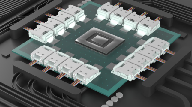
Nubis' bandwidth-packed tiny optical engine

- Nubis Communications has revealed its ambitions to be an optical input-output (I/O) solutions provider
- Its tiny 1.6-terabit optical engine measures 5mm x 7.5mm
- The optical engine has a power consumption of below 4 picojoule/bit (pJ/b) and a bandwidth density of 0.5 terabits per millimetre.
- “Future systems will be I/O with an ASIC dangling off it.”
Nubis Communications has ended its period of secrecy to unveil an optical engine targeted at systems with demanding data input-output requirements.
The start-up claims its optical engine delivers unmatched bandwidth density measured in terabits per millimetre (T/mm) and power consumption performance metrics.
“In the timeframe of founding the company [in 2020], it became obvious that the solution space [for our product] was machine learning-artificial intelligence,” says Dan Harding, the CEO of Nubis.
Company Background
Nubis has raised over $40 million, with the lead investor being Matrix Partners. Venture capital company Matrix Partners backed Acacia Communications, acquired by Cisco in 2021.
Other Nubis backers are Weili Dai, a co-founder of Marvell Technologies, and Belgium-based imec.xpand.

“We have raised enough money to get to production with our product,” says Harding, who joined Nubis in 2021 from Broadcom.
Peter Winzer is the CTO and founder of the company. Formerly at Nokia Bell Labs, Winzer was the 2018 winner of the Optica (then OSA) and IEEE Photonics Society’s John Tyndall Award for his work on coherent optical communications.
Nubis has 40 staff, mostly engineers.
“As a team, we are multidisciplinary,” says Winzer. The company’s expertise includes silicon photonics, analogue IC design including serialisers/ deserialisers (serdes), packaging – electrical and optical, and software including advanced simulation tools.
“It is all geared towards a systems solution,” says Winzer. “We are not just looking at the PIC [photonic integrated circuit] or the electronics; we have the system and the architecture in mind.”
The input-output challenge
Machine learning workloads continue to grow at a staggering pace, doubling more than twice each year. Not surprisingly, computing systems running such workloads are struggling to keep up.
Scaling such systems not only requires more processing – more graphics processing units (GPUs) – but also networking to connect clusters of GPUs.
What the compute vendors want is any-to-any connectivity between processors and between clusters. This is creating a tremendous input-output challenge in terms of bandwidth density while keeping the power consumption under control.
“Over half the power of that cluster can be taken up by traditional optics,” says Harding. “So it is clear that the industry wants new solutions.”
“Whatever cents-per-gigabit [figure] you use, if you multiply it by the I/O capacity, the number you’ll get is many times that of [the cost of] an ASIC,” adds Winzer. “We say that future systems will be I/O with an ASIC dangling off it.”

Design details
Nubis’ optical engine is a 16 x 112-gigabit design with a footprint of 5mm x 7.5mm.
“Because we have our electronics flip-chipped on top, that’s the entire footprint,” says Winzer. “We maintain that it is the highest density by far of any optical engine.”
Nubis says many parallel fibres can be interfaced to the optical engine despite its tiny size.
Supporting parallel fibres is essential for machine learning systems as the fibres are fanned out to enable any-to-any connectivity.
Nubis’ engine uses a 4 by DR4 fan-out architecture with 36 fibres arranged in a 3×12 array.
Surface coupling in a 2D array interfaces the 36 fibres to the PIC: 32 fibres are for data and four for the external laser light source.
There is only a physical limit to the number of fibres that can be connected if edge coupling is used, says Winzer. But surface coupling in a 2D array means the optical engine delivers 5-10x more density than its competitors.
The start-up also has designed the engine’s electronics: the optical modulator driver and the trans-impedance amplifier (TIA). The electronics use advanced equalisation to boost the electrical channel, given direct drive has demanding requirements, says Harding.
The XT1600 optical module
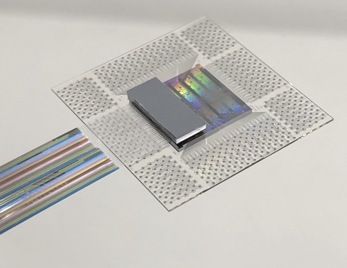
Nubis’ first product is the XT1600 optical module. Here, a substrate houses the company’s PIC and electronics onto which is packaged a lid containing the optical fibres.
Nubis has developed in-house the packaging and the fibre attach solution.
The substrate is 15x15mm, somewhat larger than the engine. Harding says this is deliberate to support products under development.
The 1.6 terabits – in fact, 16x112Gbps full duplex – module has a 2km reach. Its power consumption is below 4 pJ/b.
The fibres exit the module vertically and bend to the side. “[Going] vertical is good but the 2D is the much more important aspect here,” says Winzer.
A 2D approach is logical, says Nubis. An electrical ball grid array (BGA) all the bottom surface. It makes sense that the optics is similarly massively 2D, especially for designs where its a 100-gigabit electrical signal in and a 100-gigabit optical signal out.
Multiple rings of optical I/O engines can surround the ASIC because the fibres exit vertically. “Nobody else can do that because they are escaping from the [PIC] edge,” says Winzer.
Winzer highlights another benefit of the design.
The Universal Chiplet Interconnect Express (UCIe) specification calls for 2T/mm bandwidth escape density. An optical chiplet can only achieve this if wavelength-division multiplexing (WDM) is used due to the large fibre size. Nubis can achieve this density optically without having to use WDM because of 2D surface coupling.
Doing all-to-all at scale remains a big system challenge. “We’re just a part of that challenge,” says Harding. But for optical I/O to become pervasive in the data centre over the next five years, the optics must be significantly lower power, smaller, and efficient.
“If you crack that 2D nut, you can do many, many great things down the road,” says Winzer. “We’ve solved a huge technology problem that allows us to scale much better than anybody else.”
Status
Nubis has not named its foundry and contract manufacturing partners but says they are large, high-volume manufacturers.
Harding says there are now up to five credible silicon photonic foundries available.
“There was some early product definition which some foundries were better suited to support,“ says Harding. “And there was a robustness of the initial PDKs [process design kits] to get us an early product that was important to us.”
Choosing a contract manufacturer proved easier, given the maturity of the players.
Nubis’ first product has 16 optical channels each at 112 gigabit, but future designs will offer N by 224-gigabit channels.
Meanwhile, the XT1600 optical engine is available for sampling.

Teramount brings pluggability to co-packaged optics
Hesham Taha, the CEO and co-founder of Teramount, describes the last two years for his company as eventful.
“Many things have happened on many fronts,” he says.
Teramount has developed a fibre assembly technology for designs integrating photonics and chips.
The start-up has raised $20 million in funding and has 30 staff. In addition, the company is recruiting staff experienced in manufacturing processes.
“The funding helps to support what we are working on today, which is manufacturing readiness,” says Taha.
Taha also notes marketplace changes as when the rising interest in co-packaged caused some companies that had stepped out of silicon photonics to return.
The marketplace moves reflect silicon photonics’ changing role. The technology is central for integrated designs such as co-packaged optics, whereas before, it had a more peripheral role when used for pluggable optics.
“This is a big change that requires optical integration with electronics, a change in packaging, and how you assemble fibres,” says Taha.
Plugs and bumps
Teramount’s technology coupling fibre to silicon photonics chips has two elements: a photonic bump and a photonic plug. The two combined avoid having to bond the fibre to the chip directly.
This is important for two reasons.
First, fibre bonding is an extra manufacturing step that impacts adversely the yield of an expensive chip.
Second, the plug, which is on a separate plane from the chip, working together with the photonic bump, enables the fibres to be detached and serviced, much like pluggable optics.
The photonic plug holds the fibres using a V-groove mechanism and couples them to the silicon photonics chip via the photonic bump, a component manufactured as part of the silicon photonics design.
It is the plug and bump combined that deliver large assembly tolerances. “The large tolerances is what enables the detachability,” says Taha.
It means a semiconductor company can avoid dealing with fibres and focus on what it does best: designing chips. Foundries and outsourced semiconductor assembly and test (OSAT) companies can handle the wafer-level plug and connect the fibres.
“If the right foundations are set on the silicon photonics wafer, then silicon photonics packaging can become very easy with detachable optics,” says Taha.
Surface coupling and edge coupling
Silicon photonics uses two approaches to couple the optical signal from the fibre to a photonics chip.
One, known as surface coupling, uses a grating coupler, while the second uses side coupling.
Grating couplers are wavelength dependent and send the light beam out at a specific angle. Therefore, changing the wavelength affects the angle, complicating the interfacing.

As part of the silicon photonics chip design, the photonic bump – effectively a lens – is positioned accurately next to the grating coupler.
In contrast, side coupling collects the beam for the silicon photonic chip’s waveguide from the edge of the die. Here, there is no spectral dependency. “You can inject in and out multiple wavelengths,” says Taha.
Teramount says side coupling is not viable for the volume manufacturing of silicon photonic designs.
“You cannot connect a fibre from the edge of the die; you have to prepare for a photonic bump before wafer dicing for side coupling,” says Taha.
Teramount’s design enables light to go to the side of the die, but instead of collecting it from the edge, the photonic bump deflects the beam vertically.
“The photonic bump shifts side coupling into the wideband surface coupling,” says Taha.
The photonic bump has two components in the wideband surface coupling case: a wideband deflector and a lens mirror for beam expansion.
The photonic bump and plug combined forms what Teramount calls self-aligning optics. “You have added more complexity in wafer-level manufacturing, but you have relaxed the tolerances in the assembly domain,” he says.
The resulting design has assembly tolerances of +/- 30 microns. “Altogether, over 60 microns, you lose only half a dB in misalignment tolerances,” he says.
Teramount supports both solutions: surface coupling for a single wavelength and wideband surface coupling for multiple wavelengths. Most customers are working with the wideband solution, says Taha.
The assembly tolerances, wideband surface coupling, and planar separation of the fibres from the die, are what enable fibre detachability, says Taha.
“A technician can manually assemble hundreds of fibres on a co-packaged optics stack,” he says.
The fibre assembly process is compatible with semiconductor packaging techniques. No fibre reflow soldering is needed, improving co-packaged optics’ yield while enabling the servicing of the fibre assembly for co-packaged optics.
Status
Teramount announced in 2022 a collaboration with EV Group, an equipment and process solutions supplier, to tackle wafer-level optics.
Taha says Teramount is working with foundries, OSATs and wafer-level optics manufacturers, such as EV group, to create an ecosystem for its photonic bump and photonic plug technology.
“We want the customer to have the ability to use a foundry to include in their wafer a photonic bump,” says Taha. “Once there, a customer can enjoy the photonic plug connector, its relaxed assembly tolerances, and detachable fibre connectivity.”
Teramount is also working with vendors in networking and computing, developers of co-packaged optics and optical input-output for processor clusters used for machine learning, respectively.
“We’ve already sent samples to customers that we are working with, which includes 32 fibres,” says Taha.
Teramount intends to announce more collaborations with vendors and wafer-manufacturing suppliers.

OFC 2023 show preview
- Sunday, March 5 marks the start of the Optical Fiber Communication (OFC) conference in San Diego, California
- The three General Chairs – Ramon Casellas, Chris Cole, and Ming-Jun Li – discuss the upcoming conference
OFC 2023 will be a show of multiple themes. That, at least, is the view of the team overseeing and coordinating this year’s conference and exhibition.
General Chair Ming-Jun Li of Corning who is also the recipient of the 2023 John Tyndall Award (see profiles, bottom), begins by highlighting the 1,000 paper submissions, suggesting that OFC has returned to pre-pandemic levels.
Ramon Casellas, another General Chair, highlights this year’s emphasis on the social aspects of technology. “We are trying not to forget what we are doing and why we are doing it,” he says.
Casellas highlights the OFC’s Plenary Session speakers (see section, below), an invited talk by Professor Dimitra Simeonidou of the University of Bristol, entitled: Human-Centric Networking and the Road to 6G, and a special event on sustainability.
This year’s OFC has received more submissions on quantum communications totaling 66 papers.
In the past, papers on quantum communications were submitted across OFC’s tracks addressing networking, subsystems and systems, and devices. However, evaluating them was challenging given that only some reviewers are quantum experts, says Chris Cole, the third General Chair. Now, OFC has a subcommittee dedicated to quantum.
Another first is OFCnet, a production network that will run during the show.
Themes and topics
Machine learning is one notable topic this year. The subject is familiar at OFC, says Casellas, but people are discussing it more.
Casellas highlights one session at OFC 2021 that addressed machine learning for optics and optics for machine learning. “It showed the duality of how you can use photonic components to do machine learning and apply machine learning to optimise networking,” says Casellas.
This year there will be additional aspects of machine learning for networks, transmission, and operations, says Casellas.
Other General Chair highlighted subjects include point-to-multipoint coherent transmission, non-terrestrial and satellite networks, and optical switching and how its benefits networking in the data centre.
Google, for example, is presenting a paper detailing its use of optical switching in its data centres, something the hyperscaler disclosed at the ACM Sigcomm conference in August 2022.
There is also more interest in fibre sensors used in communications networks.
“We see an increasing trend because now if you want smart networks, you need sensors everywhere,” says Li.
“That is another theme that goes across all the tracks, which is a non-traditional optical fibre communication area that we’ve been embracing,” adds Cole.
As examples, Cole cites lidar, radio over fibre, free-space communications, microwave fibre sensing, and optical processing.
OFC has had contributions in these areas, he says, but now these topics have dedicated subcommittee titles.
Plenary session
This year’s three Plenary Session speakers are:
- Patricia Obo-Nai, CEO of Vodafone Ghana, who will discuss Harnessing Digitalization for Effective Social Change,
- Jayshree V. Ullal, president and CEO of Arista Networks, addressing The Road to Petascale Cloud Networking,
- and Wendell P. Weeks, chairman and CEO of Corning, whose talk is entitled Capacity to Transform.
“We thought that having someone who could explain how technology improves society would be very positive,” says Casellas. “I’m proud to have someone who can talk on the benefits of digitisation from the point of view of society, in addition to more technical topics.”
Li highlights how OFC celebrated the 50th anniversary of low-loss fibre two years ago and that last year, OFC celebrated the year of glass, displaying information on panels.
Corning has played an important role in both technologies. “Having a speaker [Wendell Weeks] from a glass company talking about both will be interesting to the OFC audience,” says Li.
Cole highlights the third speaker, Jayshree Ullal, the CEO of Arista. The successful networking player is one of the companies competing in what he describes as a very tough field.
Rump session
This year’s Rump Session tackles silicon photonics, a session moderated by Daniel Kuchta of IBM TJ Watson Research Center and Michael Hochberg of Luminous Computing.
Cole says silicon photonics has received tremendous attention, and the Rump Session is asking some tough questions: “Is silicon photonics for real now? Is it just one of the guys in the toolbox? Or is it being sunsetted or supplemented?”
Cole expects a lively session, not just challenging conventional thinking but having people representing exciting alternatives which are commercially successful alongside silicon photonics.
Show interests
The Chairs also highlight their interests and what they hope to learn from the show.
For Li, it is high-density fibre and cable trends.
Work on space division multiplexing (SDM) – multicore and multimode – fibre has been an OFC topic for over 15 years. One question Li has is whether systems will use SDM.
“It looks like multicore fibre is close, but we want to learn more from customers,” says Li.
Another interest is an alternative development of reduced coating diameter fibres that promise greater cable density. “I always think this is probably the short-term solution, but we’ll see what people think,” says Li.
AI drives interest in fibre density and latency issues in the data centre. Low latency is attracting interest in hollow-core fibre. Microsoft acquired Lumenisity, a UK hollow core fibre specialist, late last year.
Li is keen to learn more about quantum communications. “We want to understand, from a fibre component point of view, what to do in this area.”
Until now industry focus has been on quantum key distribution (QKD), but Li wants to learn about other applications of quantum in telecoms.
The bandwidth challenge facing datacom is Cole’s interest.
As the Rump Session shows, there has been an explosion of technologies to address data challenges, particularly in the data centre. “So I’m looking forward to continuing to see all the great ideas and all the different directions,” says Cole.
Another show interest for Cole is start-ups in components, subsystems and systems, and networking.
At Optica’s Executive Forum, held on Monday, March 6, a session is dedicated to start-ups. Casellas is looking forward to the talks on optical network automation.
Much work has applied machine learning to optical transmission and amplifier optimisation. Casellas wants to see how reinforcement learning is applied to optical network controllers. Telemetry and its use for network monitoring are another of his interests.
“Maybe because I’m an academic and idealistic, but I like everything related to disaggregation and the opening of interfaces,” says Casellas, who too wants to learn more about quantum.
“I have a basic understanding of this, but maybe it is hard to get into something new,” says Casellas. Non-terrestrial and satellite networks are other topics of interest.
Cole concludes with a big-picture view of photonics.
“It’s a great time to be in optics,” he says. “We’re seeing an explosion of creativity in different areas to solve problems.”
Ramon Casellas works at the Centre Tecnològic de Telecomunicacions de Catalunya (CTTC) research institution in Barcelona, Spain. His research focuses on networks – particularly the control plane, operations and management – rather than optical systems and devices.
Ming-Jun Li is a Corporate Fellow at Corning where he has that worked for 32 years.
Li is also this year’s winner of the John Tyndall Award, presented by Optica and the IEEE Photonics Society. The award is for Li’s ‘seminal contributions to advances in optical fibre technology.’
“It was a surprise to me and a great honour,” says Li. “The work is not only for myself but for many people working with me at Corning; I cannot achieve without working with meaningful colleagues.”
Chris Cole is a consultant whose background is in datacom optics. He will be representing the company, Coherent, at OFC.
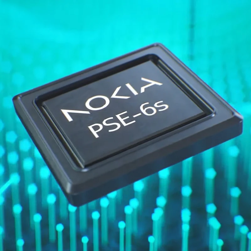
Nokia jumps a class with its PSE-6s coherent modem
- The 130 gigabaud (GBd) PSE-6s coherent modem is Nokia’s first in-house design for high-end optical transport systems
- The PSE-6s can send an 800 gigabit Ethernet (800GbE) payload over 2,000km and 1.2 terabits of data over 100km.
- Two PSE-6s DSPs can send three 800GbE signals over two 1.2-terabit wavelengths
Nokia has unveiled its latest coherent modem, the super coherent Photonic Service Engine 6s (PSE-6s) that will power its optical transport platforms in the coming years.
The PSE-6s comes three years after Nokia announced its current generation of coherent digital signal processors (DSPs): the PSE-Vs DSP for the long-haul and the compact PSE-Vc for the coherent pluggable market.
Nokia is only detailing the PSE-6s; its next-generation coherent modem for pluggables will be a future announcement.
Nokia will demonstrate the PSE-6s at the upcoming OFC show in March while field trials involving systems using the PSE-6s will start in the year’s second half.
Reducing cost per bit
In 2020, Nokia bought Elenion, a silicon photonics company specialising in coherent optics.
The PSE-6s is Nokia’s first in-house coherent modem – the coherent DSP and associated optics – targeting the most demanding optical transport applications.
Nokia points out that coherent systems started approaching the Shannon limit two generations ago.
In the past, operators could reduce the cost of optical transport by sending more data down a fibre; upgrading the optical signal from 100 to 200 to 400 gigabit required only a 50GHz channel.
“You were getting more fibre capacity with each generation,” says Serge Melle, director of product marketing, optical networks at Nokia. And this helped the continual reduction of the cost-per-bit metric.
But with more advanced DSPs, implemented using 16nm, 7nm, and now 5nm CMOS, going to a higher symbol rate and hence data rate requires more spectrum, says Melle.
Increasing the symbol rate is still beneficial. It allows more data to be sent using the same modulation scheme or transmitting the same data payload over longer distances.
“So one of the things we are looking to do with the PSE-6s is how do we still enable a lower total cost of ownership even though you don’t get more capacity per wavelength or fibre,” says Melle.

Symbol rate classes
Coherent optics from the leading vendors use a symbol rate of 90-107 gigabaud (GBd), while Cisco-owned Acacia’s latest 1.2-terabit coherent modem in a CIM-8 module operates at 140GBd.
Acacia uses a classification system based on symbol rate. First-generation coherent systems operating at 30-34GBd are deemed Class 1. Class 2 doubles the baud rates to 60-68GBd, the symbol rate window used for 400ZR coherent optics, for hyperscalers to connect equipment across their data centres up to 120km apart.
The DSPs from the leading optical transport systems vendors operating at 90-107GBd are an intermediate step between Class 2 and Class 3 using Acacia’s classification. In contrast, Acacia has jumped directly from Class 2 to Class 3 with its 140GBd CIM-8 coherent modem.
Competitors view Acacia’s classification scheme as a marketing exercise and counter that their 90-107GBd optical transport systems benefited customers for over two years.
Nokia’s 90GBd PSE-Vs can send 400 gigabits using quadrature phase-shift keying (QPSK) over 3,000km. This contrasts with its earlier 67GBd PSE-3s that sends 400GbE up to 1,000km using 16-QAM.
However, with the PSE-Vs, Nokia, unlike its optical transport competitors, Infinera, Ciena and Huawei, decided not to support 800-gigabit wavelengths.
Nokia argued that 7nm CMOS, 90-100GBd coherent optics tops out at 600 gigabit when used for distances of several hundred kilometers, while metro-regional distances are more economically served using 400-gigabit pluggable optics such as the CFP2 implementing 400ZR+.
With the 130Gbd PSE-6s, Nokia has a Class 3 coherent modem with the PSE-6s capable of sending 800 gigabits more than 2,000km.
The PSE-6s also doubles the maximum data rate of the PSE-Vs to 1.2 terabits per wavelength. However, at 1.2 terabits, the reach is 100-plus km, valuable for very high capacity metro transport and data centre interconnect.
Scale, reach and power consumption per bit
Nokia highlights the PSE-6s’ main three performance metric improvements.
First, the coherent modem delivers scaling: two coherent optical engines fit on a line card to deliver 2.4 terabits to transport emerging high-speed services such as 800GbE.
The two PSE-6s are linked using a dedicated interface to share the client-side signals (see diagram).
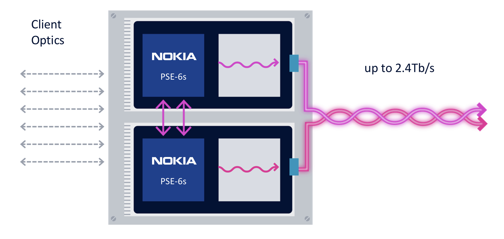
“We are not the only ones introducing a 5nm solution, but I think we are the only ones that allow two DSPs to work together,” says Melle.
Without the interface, a single 800GbE and up to four 100GbE clients or a 400GbE client can be sent over each DSP’s 1.2-terabit wavelength. Adding the interface, an operator can send three uniform 800GbE clients, with the interface splitting the third 800GbE client between the two DSPs.
“In a single line card, you can stripe the three 800-gigabit services rather than have to deploy three separate line cards in the network,” says Melle.
Nokia is not detailing the interface used to link the DSPs but said that the interface is used for data only and not to share signal processing resources between the ASICs.
“There is an extra amount of circuitry to share the client bandwidth across the two DSPs, but it is not high power consuming, and most transponders have some circuitry between the clients and the DSP,” says Melle. “So the incremental ‘power tax’ is marginal; it doesn’t add any significant power overhead.”
The resulting 2.4-terabit transmission is sent as two 1.2-terabit wavelengths, each occupying a 150GHz-wide channel. Existing systems that operate at 90-107GBd typically use a 112.5GHz channel for an 800-gigabit transmission, so the PSE-6s delivers a fibre capacity benefit.
The two wavelengths can be bonded, as in a two-channel ‘super-channel’, or sent to separate locations.
The second improvement is optical performance. For example, an 800-gigabit payload can travel over 2,000km. Nokia claims this is 3x the reach of existing commercial optical transport systems.
The improved transmission performance is achieved using a combination of the 130GBd baud rate, probabilistic constellation shaping (PCS), and improved forward error correction (FEC). Melle says the contributions to the improvement are 90 per cent baud rate and 10 per cent due to coherent modem algorithm tweaks.
“Baud rate is king; that is what really drives this improved performance,” says Melle.
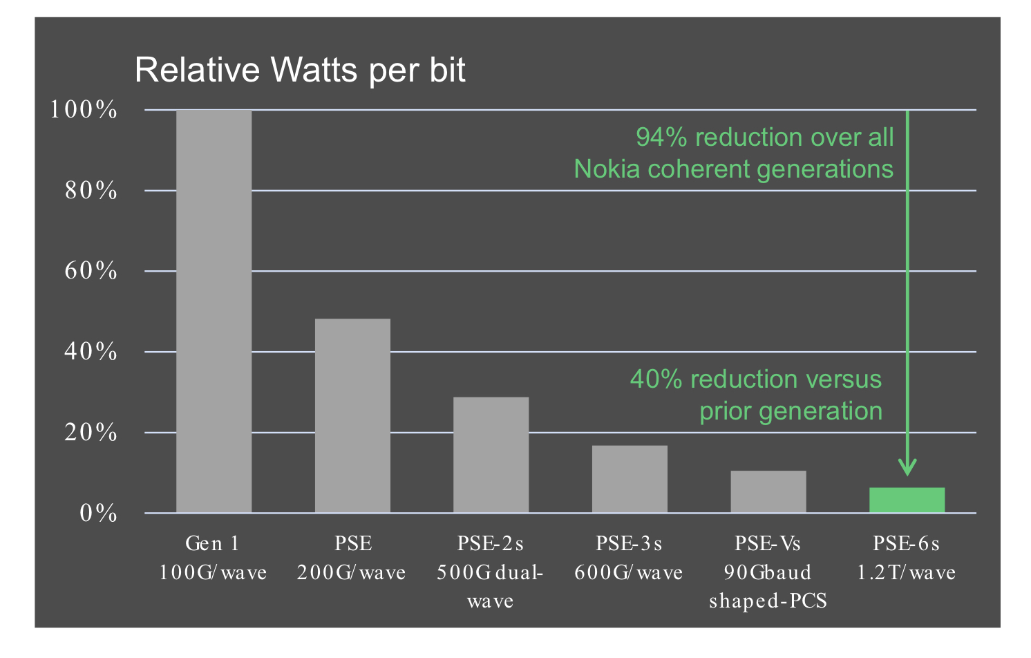
The third benefit is reduced power consumption at the device and system (networking) levels.
Using a 5nm finFET CMOS process to make the PSE-6s DSP ASIC and developing denser line cards (two modems per card) means systems will consume 60 per cent less power than Nokia’s existing coherent technology.
According to Nokia, the PSE-6s optical engine consumes 40 per cent fewer Watts per bit compared to the PSE-Vs.
Nokia 1830 transport systems
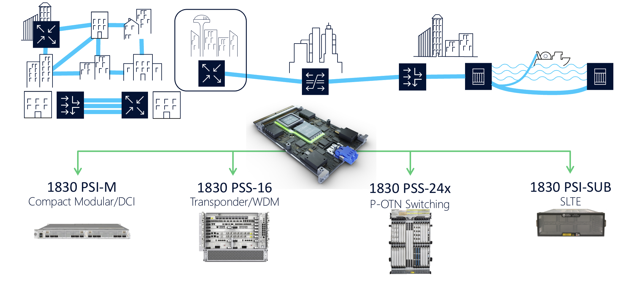
The PSE-6s line cards fit into Nokia’s existing range of 1830 transport platforms.
These include the 1830 PSI-M compact modular data centre interconnect, the 1830 PSS-16 transponder and WDM line system, the 1830 PSS-24x P-OTN and switching chassis, and the 1830 PSI-SUB subsea line-terminating equipment.
For example, the PSI-M platform can hold two line cards, each with two PSE-6s.
How to shepherd a company’s technologies for growth

CTO interviews part 3: Dr Julie Eng
- Eng is four months into her new role as CTO of Coherent.
- Previously, she headed Finisar’s transceiver business and then the 3D sensing business, first at Finisar and then at II-VI. II-VI changed its name to Coherent in September 2022
- “CTO is one of these roles that has no universal definition,” says Eng
ulie Eng loved her previous role.
She had been heading II-VI’s (now Coherent’s) 3D sensing unit after being VP of engineering at Finisar’s transceiver business. II-VI bought Finisar in 2019.
She moved across to a new 3D sensing business while still at Finisar. The 3D sensing unit was like a start-up within a large company, she says.
II-VI and Finisar had been competitors in the 3D sensing market. Eng headed the combined units after Finisar’s acquisition.
She enjoyed the role and wasn’t looking to change when the CEO asked her to become Coherent’s CTO.
“To become CTO of the new Coherent – to help define the future of this company which is a five-plus going on six billion dollar company – that is pretty exciting,” says Eng.
The “New” Coherent
Coherent combines a broad portfolio of technologies from II-VI, Finisar, and the firm Coherent which II-VI acquired in 2022.
Just within lasers, Coherent’s portfolio spans from devices 1mm wide that are sold into mobile phones to the former Coherent’s lasers that are meters wide and used for OLED manufacturing.
Being CTO is different from Eng’s line-management roles, which had set, tangible annual goals.
Her role now is to shepherd the company’s technologies and grow the business over the long term.
Eng has been familiarising herself with the company’s technologies. To this aim, Eng is drawing on deep technological expertise across the company’s units.
Luckily, lasers are already covered, she quips.
“One of the things that I always somehow had a knack for is interacting with customers, sensing opportunities, and then figuring out how our technologies can help customers solve their problems,” says Eng.
It is a skill she successfully transferred to the consumer – 3D sensing – business but now it will be needed on a broader scale.
Eng is also making connections across technology units within the company as she seeks to identify new technologies and new market opportunities.
Her CTO role also allows her to engage with every Coherent customer across the company’s many markets.
She admits being CTO is challenging. One issue is grappling with the breadth of technologies the company has. Another is how to assess her works’ impact.
She and the CEO have discussed how best to use her time to benefit the company. Eng has also talked to other companies’ CTOs about the role and what works for them.
“It’s very interesting; CTO is one of these roles that has no universal definition,” says Eng.
Technologies to watch
Eng highlights several developments when asked about noteworthy technologies.
For communications, this is the year when 200 gigabits per lane will likely be achieved.
“The first transceivers I worked on were [SONET/SDH] OC-3 which is 155 megabits per second (Mbps),” she says. “Is wasn’t even a transceiver back then; it was discrete transmitters and receivers.”
That the industry has accelerated technology to achieve multiple lanes of 200 gigabit-per-second (Gbps) in a pluggable module is remarkable, she says.
Eng also notes Coherent’s work on a continuous-wave laser integrated with a Mach-Zehnder modulator – a DMZ – to enable 200 gigabits per lane.
The company is also active in life sciences and health monitoring. Communications, especially during the pandemic, showed its importance in people’s lives. “But life sciences and health-related products have a much more direct impact on people,” says Eng. “That is not something I’ve had direct exposure to.”
Life sciences and health monitoring is a segment where optics and optical devices will play a growing role over time.
Medical devices often originate in research environments such as hospital labs before becoming medical instruments. From the lab, they go to clinical. “What we are talking about here is going from lab to clinical to therapeutics,” she says.
The US Chips Act also heartens Eng: “It was about time for the US to prioritise semiconductors.”
Low-power coherent DSPs
Coherent and ADVA jointly developed a low-power coherent digital signal processor (DSP) and optics design for a 100-gigabit ZR (100ZR) design that fits within a QSFP28 module.
“We have an internal DSP team, and they are developing DSPs for the coherent optics market,” says Eng, adding that having the design team gives Coherent options.
Meanwhile, the debate about direct detection technology versus coherent optics continues.
As optical lane speed increases from 100 gigabits to 200 gigabits, the question remains what reach will direct detection achieve before running out of steam?
With 200 gigabits per lane, 800 gigabit modules can be achieved using four optical lanes, while for 1.6 terabits, eight lanes will be used.
Eng is confident that direct detection will support 10km at these speeds. Beyond 10km, direct detection becomes much more of a challenge, and coherent is an option.
“The real question is will coherent optics meet the size, cost and power consumption expectations of the data centre customers on a timeframe that meets their needs,” says Eng.
Having in-house DSP technology means Coherent can undertake design trade-offs and make the right decisions, she says.
After 1.6 terabits, the design options include increasing the lane rate, using more than eight channels or adopting more advanced modulation schemes.
“We look at the application, the timeline that the product needs to be released, the readiness of the technology, we do measurements – simulations – and we make objective decisions based on the results,” says Eng.
Whatever the prevalent technology is, says Eng, that technology will continue to improve since that is the livelihood of many companies.
“All of us, as an industry, are going to put our all into extending the technologies we currently have,” says Eng. So, when it comes to direct detection versus coherent, everyone will push direct detect technology as far as possible.
“Getting up to 1.6 terabits [using direct detect], that is pretty good,” says Eng. “That is going to last us a pretty long time.”
Materials
Coherent’s toolbox of material systems covers indium phosphide, silicon photonics, and gallium arsenide. It also has silicon carbide, a semiconductor suited for high-power transistors used for power electronics applications.
“We have all the technologies, we use the best technology for the product, and we use good engineering judgement,” says Eng.
Rather than favour indium phosphide or silicon photonics, Eng’s segmentation starts with whether the design is directly modulated or externally modulated.
Until now, up to 50 gigabits per lane has been well served by directly modulated lasers. This has used indium phosphide or, in the case of VCSELs, gallium arsenide.
“In general, directly modulated is the lower cost because the die is tiny, and often it is the lowest power,” says Eng.
But increasing the speed beyond 50Gbps gets more complicated with directly modulated lasers. This is where externally modulated lasers come in.
“Once you are already talking about an externally modulated solution, we start looking at the trade-offs between indium phosphide and silicon photonics,” says Eng.
The laser remains indium phosphide, so the bake-off concerns the modulator and the passive optics.
What indium phosphide brings is better electro-optics performance, while silicon photonics brings the benefits of integration.
“So if there is a high-lane count – lots of passives – or an opportunity to use one laser over multiple modulators, these can be complicated designs, and silicon photonics can help reduce the size,” says Eng.

Pluggables and co-packaged optics
With 200 gigabits per lane becoming available, there is a clear roadmap for 800-gigabits and 1.6-terabit pluggables.
“Customers like pluggables, and I don’t think people should underestimate that,” says Eng, adding that continued innovation will extend their lifetime.
“There are flyover cables between the switch ASIC and the modules, vertical line cards have been proposed, and we have shown board-mounted optical assemblies,” she says.
At some point, co-packaged optics may be the right solution, says Eng. But that will depend on the application’s specification, issues such as bandwidth, size, cost, power consumption and reliability.
“People will only transition to optical input-output when extending pluggables doesn’t make sense anymore,” says Eng. “I think it is probably five-plus years away, but there are probably error bars on that.”
Coherent’s activities include using indium phosphide manufacturing for external laser sources for co-package optics. “And we are working on silicon photonics,” she says.
Coherent is also working on co-packaging VCSELs with high-performance chips. “Not all applications require a 2km reach,” she says.

The coming decade’s opportunities
Eng’s thoughts about the growth opportunities for the coming decade are, not surprisingly, viewed through Coherent’s markets focus.
She highlights four segments: communications, industrial, instrumentation, and electronics.
Fibre-optics communications will continue to grow with bandwidth. The opportunities for innovation include datacom and coherent optics.
She also notes growing interest in free-space optics and satellite communications.
“I see money being spent on that and maybe that is a place where someone like ourselves, with a lot of optics as well as bigger lasers, can play a role,” says Eng.
Precision manufacturing uses lasers in the industrial segment. Eng cites cutting, welding and marking as examples.
“We have elements used for battery manufacturing which is increasing due to electric cars,” she says.
Excimer lasers are also used for OLED and microLED display manufacturing.
“We even have optics in extreme UV steppers [used for advanced process node chip manufacturing],” she says.
For instrumentation, much of the growth is around health life sciences. Coherent makes optics that are used inside PCR testers for COVID-19. It also has engineers working on solid state lasers used for flow cytometry (the sorting of cells). She also cites gene sequencing equipment and medical imaging.
Coherent’s electronics segment refers to the consumer market. Growth here for optics and lasers include AR/VR goggles and the metaverse, wearable health monitoring, and automotive.
For automotive, lasers are used for lidar and in-cabin sensing, such as driver and passenger monitoring.
Silicon carbide is also a growth market, and its uses include the wireless market and power devices for electric vehicles.
“I like the communications market, which we see as growing, but for us, with such a broad portfolio, there are many of these other markets and products that I see as exciting for the remainder of this decade,” says Eng.

Microchip expands the choice of 1.6-terabit Ethernet PHYs
Microchip Technology has enlarged its portfolio of 1.6-terabit physical layer (PHY) Ethernet chips targeting next-generation switch and router line cards.
In 2021, Microchip announced its PM6200 Meta-DX2L (‘L’ standing for light), its first 1.6-terabit Meta-DX2 PHY that uses 112-gigabit PAM-4 (4-level pulse-amplitude modulation) serialiser/ deserialisers (series).
Microchip has now added four more 1.6-terabit Ethernet PHYs dubbed Meta-DX2+.
Like the Meta-DX2L, the PHYs are implemented using a 6nm CMOS process while the ‘plus’ signifies added features.
The Meta-DX2L is used for such tasks as retiming, for a signal sent across the system’s backplane, for example, and has a ‘gearbox’ feature that translates between 28, 56 and 112-gigabit data rates.
With the Meta-DX2+ PHYs, Microchip has added port aggregation and security hardware.

Security and flexibility
Microchip stresses the compact nature of its 1.6-terabit PHYs.
”We see that [compactness] as very important to our customers as they seek to double capacity and design dense systems,” says Stephen Docking, senior manager of product marketing, communications business unit at Microchip.
Security is important for cloud and enterprise, and Microchip claims it has the first PHYs supporting 1.6-terabit of capacity with MACsec and IPsec.
MACsec is used to secure traffic between distributed data centre buildings across a campus or a metropolitan region. IPsec is used for enterprise-wide area networks (WANs) where traffic goes through nodes, some of which may not support encryption.
“The intention is that we can offload those encryption engines having to be in a packet processor or switch device in a system,” says Docking.
The Meta-DX2 1.6-terabit PHYs can interface with 400-gigabit client-side pluggables, emerging 800 gigabit QSFP-DD800s, and upcoming 1.6-terabit OSFP-XD optical modules.
The 1.6 terabit PHYs effectively have two 800-gigabit cores that support rates from 1 to 800 Gigabit Ethernet.
One-gigabit Ethernet is supported as it is still used by enterprises, while 800-gigabit is soon to be deployed, says Docking.
Enterprises also require new switch devices so the 112-gigabit serdes is necessary, but many sub-100 gigabit rates remain in use. Microchip has added its XpandIO feature that aggregates low-speed ports – 1GbE, 10GbE, 25GbE, 50GbE – into the 112-gigabit PAM-4 lane to improve system efficiency.
New packet processor designs have 112-gigabit serdes. If lower rate speeds are fed directly to the packet processor, bandwidth is wasted. Microchip’s XpandIO feature aggregates these lower rates to better match the packet processor’s serdes speed.
The Meta-DX2+ PHY, like the Meta-DX2L, also feature a hitless 2:1 multiplexer. The multiplexer function is suited for central architecture switch platforms where the system intelligence resides on a central card. In contrast, the connecting line cards are relatively simple, comprising PHYs and optical modules.
In such systems, because of the central role of the platform’s switch card, a standby card is included. If the primary card fails, the backup card kicks in, whereby all the switch’s line cards connect to the backup. The 2:1 multiplexer feature in the PHY means each line card is interfaced with both switch cards: the primary and the backup.
The Meta-DX2 PHY family
The Meta-DX2 PHYs are split into two groupings, the PHYs in each group are hardware compatible such that one line card design is needed.
One group has three PHYs: the PM6200 (the Meta-DX2L), the PM6216 (the Meta-DX2+ PHY with encryption engines), and the PM6210 (a Meta-DX2+ with encryption and XpandIO). All three measure 23x30mm.
The two other Meta-DX2+ PHYs – the PM6214 and the PM6218 (with encryption) – are larger ICs, 33x33mm. This is because the PHYs have 48, 100-gigabit serdes instead of 32 serdes of the first group.
The extra 16 100-gigabit serdes enable the PHYs to support, for example, 16 100-gigabit lanes (1.6-terabit) when connected to a switch IC as well as 32 lanes of 50-gigabit serdes used in 8×50-gigabit 400-gigabit QSFP-DD modules.
“The PHY package size, in this case, is larger,” says Docking. “But even with that, we still have a net 20 per cent reduction in total area.” That can make a difference between fitting in a one rack unit (1RU) design rather than 2RU.
All PHYs share a common software development kit. The software kit also supports the switch abstraction interface standard. “This decouples the operating systems from the underlying hardware,” says Dorking.
The Meta-DX2+ PHYs have been sampling since the final quarter of 2022 and the chips are available for prototypes.
Applications
The PHY portfolio caters for several classes of system designs. Microchip cites cloud and enterprise data centre switches and routers, service provider routers, encryption boxes, and optical transport platforms.

Microchip says that the Meta-DX2L was released to address the first generation of higher capacity line cards where retiming and gearbox rate changes are essential.
The remaining 1.6-terabit PHYs available now better address system vendors’ second-generation card designs that typically add features such as encryption.
What next?

A next obvious PHY family will be when the 224-gigabit electrical interface becomes available.
Microchip says it has invested more in this generation of 112-gigabit series-based PHYs than previous generations and it expects 112-gigabit serdes to be more of a ‘workhorse’ than in the past.
“I think what you will find is more 112-gigabit based solutions rather than every new investment cycle being a new line rate,” says Kevin So, director, product line management and marketing, communications business unit at Microchip.
It will not be the cadence of investments that changes, rather those investments will likely be anchored around the 112-gigabit electrical interface.