DustPhotonics readies its first optical engine
- DustPhotonics has a silicon photonics modulator capable of 200 gigabits per lane
- The start-up also has developed a precision laser-attach scheme
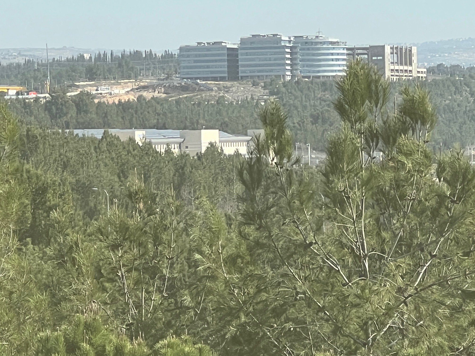
Ronnen Lovinger waves as he approaches the local train station. DustPhotonics’ CEO is taking me to the company’s offices on the outskirts of Modi’in, halfway between Tel Aviv and Jerusalem.
The site has a striking view of a landscape also halfway between Israel’s flat coastal plain and the steep hills of Jerusalem.
Lovinger has been CEO of DustPhotonics since 2021. Before that, he was chief operating officer (COO) at Innoviz Technologies, joining the lidar firm after 18 years at Mellanox, now part of Nvidia.
Strategic pivotStrategic pivot
DustPhotonics was founded in 2017 and has a staff of 46, 30 being R&D engineers.
The company began by developing multi-mode short-reach, up to 100m, optical transceivers and cables, first at 100 gigabits and then at 400 gigabits.
The start-up also made a single-mode transceiver using discrete components. The company planned to develop an integrated version using silicon photonics, a programme it started in 2018.
DustPhotonics gained a significant design win for its multi-mode transceiver with a customer who was to also act as its channel to market. DustPhotonics then spent two years investing in a high-volume production line in Thailand.
But the anticipated high-volume orders failed to materialise. “After those two years, we shipped 1,000s, not 100,000s of units,” says Lovinger. “It wasn’t the customer’s fault; the market where we had differentiation changed.”

DustPhotonics was forced to change tack. Instead of making modules, it decided to use its silicon photonics expertise to make optical engines.
“Silicon photonics is a very flexible platform, and you can integrate different technologies as well,” says Yoel Chetrit, CTO and vice president of R&D at DustPhotonics. “This gives us a roadmap that is not limited by the standard bandwidth restriction.”
Now the start-up has a 400-gigabit DR4 optical engine, dubbed Carmel, whose qualification is expected to be completed this month. Two DR4 engines enable an 800-gigabit DR8 that fits in an OSFP module.
Lovinger says that at the upcoming OFC show, to be held in March, the company will provide details to customers about the Carmel 8, a single-chip optical engine for 800G DR8 that is small enough to fit within a QSFP-DD module.
DustPhotonics also offers design services. The company it chooses only those projects that promise new markets and customers.
DustPhotonics’s chairman is Avigdor Willenz, a noted Israeli entrepreneur who founded Galileo Technology, was acquired by Marvell, and was chairman of such firms as Annapurna Labs, bought by Amazon, and AI chip company, Habana Labs, bought by Intel.
“He has been in the networking industry for over 30 years,” says Lovinger. “He knows how the architecture of the data centre looks now and how it will be in the future.”
Willenz also has contacts at key large companies and the hyperscalers. “He gets DustPhotonics a foot in the door,” says Lovinger.
1.6 terabit direct-detect modules
DustPhotonics is competing with much larger photonics players that have silicon photonics and indium-phosphide and can make their lasers. These players also sell optical transceivers.
Lovinger stresses that DustPhotonics has its strengths.
“Silicon photonics is a very difficult technology; the bar is very high in the expertise you need,” he says. “Many [firms] are trying, but it is difficult to get there.”
The company has developed a precision laser-attach scheme to the photonic integrated circuit (PIC) that has a sub-micron accuracy. The scheme results in the efficient coupling of light to the PIC. The company uses standard off-the-shelf continuous-wave lasers operating at 1310nm.
The efficiency of the laser attach scheme means two lasers can power an eight-channel design, reducing cost and overall power consumption, says Chetrit.
The company also has a highly stable silicon-photonics modulator that does not need to be temperature controlled and will operate at 200 gigabits per lane.
There is an ongoing industry debate as to whether direct-detect designs can meet all the reaches – 500m, 2km, and 10km – for next-generation 1.6-terabit (8x200Gbps) optical modules. If not, coherent optics will be needed.
“[Achieving] The 2km reach is really a challenge of power and the quality of the modulation,” says Chetrit. DustPhotonics says its direct-detect optical engines will support 1.6-terabit optical modules with a 2km reach.
At last year’s OFC (2022), hyperscalers wondered whether a ‘coherent-light’ design would be needed, says Lovinger: “But things have changed this year; 200 gigabit-per-lane direct detect will happen.”
Two hyperscalers have told DustPhotonics that if it can do this, it will be a game-changer.
“We looked at direct detect versus coherent, and there is no question, going to coherent is just too expensive and too power-hungry,” says Lovinger, adding that using coherent would double costs.
Status
DustPhotonics’ optical engines will be targeted at two markets. One is for pluggable module makers; the other is to supply physical layer (PHY) chip companies that also want optical engines to expand their product portfolio offerings.
The company also offers design capabilities, from photonic elements to complete products. “We don’t call ourselves an [optical] ASIC company, but it may be a similar model,” says Lovinger.
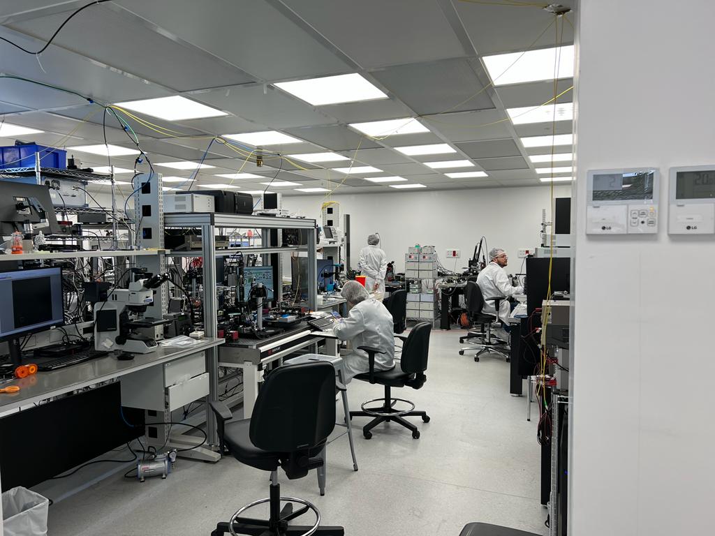
The meeting ends with a quick tour of DustPhotonics’ labs. It is here that R&D takes place, and the lab can sample build up to 1,000 optical engine products a month.
DustPhotonics recently chose Fabrinet as the outsourced assembly and test (OSAT) company. It will do the wafer dicing, burn-in, testing and packaging which will allow for production volumes much higher than in the DustPhotonics lab.
Tower Semiconductor is the silicon photonics foundry DustPhotonics is using.
“When we selected them, Tower had a mature PDK (process design kit), a very flexible process we can work with,” says Chetrit.
The industrial park where DustPhotonics is located is relatively quiet while down the road there is a much busier one. But DustPhotonics chose this one, says Lovinger, and the staff like it here. This is understandable, seeing the views from the elevated office terrace.
Lovinger then drives me to the station in time for my train to Tel Aviv and beyond.

Deutsche Telekom explains its IP-over-DWDM thinking
Telecom operators are always seeking better ways to run their networks. In particular, operators regularly scrutinise how best to couple the IP layer with their optical networking infrastructure.
The advent of 400-gigabit coherent modules that plug directly into an IP router is one development that has caught their eye.
Placing dense wavelength division multiplexing (DWDM) interfaces directly onto an IP router allows the removal of a separate transponder box and its interfacing.
IP-over-DWDM is not a new concept. However, until now, operators have had to add a coherent line card, taking up valuable router chassis space.

Now, with the advent of compact 400-gigabit coherent pluggables developed for the hyperscalers to link their data centres, telecom operators have realised that such pluggables also serve their needs.
BT will start rolling out IP-over-DWDM in its network this year, while Deutsche Telekom has analysed the merits of IP-over-DWDM.
“The adoption of IP-over-DWDM is the subject of our techno-economical studies,” says Werner Weiershausen, senior architect for the transport network at Deutsche Telekom.
Network architecture
Deutsche Telekom’s domestic network architecture comprises 12 large nodes where IP and OTN backbones align with the underlying optical networking infrastructure. These large nodes – points of presence – can be over 1,000km apart.
Like many operators, Deutsche Telekom has experienced IP annual traffic growth of 35 per cent. The need to carry more traffic without increasing costs has led the operators to adopt coherent technology, with the symbol rate rising with each new generation of optical transport technology.
A higher channel bit rate sends more data over an optical wavelength. The challenge, says Weiershausen, is maintaining the long-distance reaches with each channel rate hike.
Deutsche Telekom’s in-house team forecasts that IP traffic growth will slow down to a 20 per cent annual growth rate and even 16 per cent in future.
Weiershausen says this is still to be proven but that if annual traffic growth does slow down to 16-20 per cent, bandwidth growth issues will remain; it is just that they can be addressed over a longer timeframe.
Bandwidth and reach are long-haul networking issues. Deutsche Telekom’s metro networks, which are horse-shoe-shaped, have limited spans overall.
“For metro, our main concern is to have the lowest cost-per-bit because we are fibre- and spectrum-rich, and even a single DWDM fibre pair per metro horseshoe ring offer enough bandwidth headroom,” says Weiershausen. “So it’s easy; we have no capacity problem like the backbone. Also there, we are fibre-rich but can avoid the costly activation of multiple parallel fibre trunks.”
IP-over-DWDM
IP-over-DWDM is increasingly associated with adding pluggable optics onto an IP core router.
“This is what people call IP-over-DWDM, or what Cisco calls it hop-by-hop approach,” says Dr Sascha Vorbeck, head of strategy and architecture IP-core & transport networks at Deutsche Telekom.

Cisco’s routed optical networking – its term for the hop-by-hop approach – uses the optical layer for point-to-point connections between IP routers. As a result, traffic switching and routing occur at the IP layer rather than the optical layer, where optical traffic bypass is performed using reconfigurable optical add/drop multiplexers (ROADMs).
Routed optical networking also addresses the challenge of the rising symbol rate of coherent technology, which must maintain the longest reaches when passing through multiple ROADM stages.
Deutsche Telekom says it will not change its 12-node backbone network to accommodate additional routing stages.
“We will not change our infrastructure fundamentally because this is costly,” says Weiershausen. “We try to address this bandwidth growth with technology and not with the infrastructure change.”
Deutsche Telekom’s total cost-of-ownership analysis highlights that optical bypass remains attractive compared to a hop-by-hop approach for specific routes.
However, the operator has concluded that the best approach is to have both: some hop-by-hop where it suits its network in terms of distances but also using optical bypass for longer links using either ROADM or static bypass technology.
“A mixture is the optimum from our total cost of ownership calculation,” says Weiershausen. “There was no clear winner.”
Strategy
Deutsche Telecom favours coherent interfaces on its routers for its network backbone because it wants to simplify its network. In addition, the operator wants to rid its network of existing DWDM transponders and their short reach – ‘grey’ – interfaces linking the IP router to the DWDM transponder box.
“They use extra power and are an extra capex [capital expenditure] cost,” says Weiershausen. “They are also an additional source of failures when you have in-line several network elements. That said, heat dissipation of long-reach coherent optical DWDM interfaces limited the available IP router interfaces that could have been activated in the past.
For example, a decade ago, Deutsche Telecom tried to use IP-over-DWDM for its backbone network but had to step back to use an external DWDM transponder box due to heat dissipation problems.
The situation may have changed with modern router and optical interface generations, but this is under further study by Deutsche Telecom and is an essential prerequisite for its evolution roadmap.
Deutsche Telecom is still using traditional DWDM equipment between the interconnection of IP routers with grey interfaces. Deutsche Telecom undertook an evaluation in 2020 and calculated a traditional DWDM network versus a hop-by-hop approach. Then, the hop-by-hop method was 20 per cent more expensive. Deutsche Telecom plans to redo the calculations to see if anything has changed.
The operator has yet to decide whether to adopt ZR+ coherent pluggable optics and a hop-by-hop approach or use more advanced larger coherent modules in its routers. “This is not decided yet and depends on pricing evolution,” says Weiershausen.
With the volumes expected for pluggable coherent optics, the expectation is they will have a notable price advantage compared to traditional high-performance coherent interfaces.
But Deutsche Telekom is still determining, believing that conventional coherent interfaces may also come down markedly in price.
SDN controller
Another issue for consideration with IP-over-DWDM is the software-defined networking (SDN) controller.
IP router vendors offer their SDN controllers, but there also is a need for working with third-party SDN controllers.
For example, Deutsche Telekom is a member of the OpenROADM multi-source agreement and has pushed for IP-over-DWDM to be a significant application of the MSA.
But there are disaggregation issues regarding how a router’s coherent optical interfaces are controlled. For example, are the optical interfaces overseen and orchestrated by the OpenROADM SDN controller and its application programming interface (API) or is the SDN controller of each IP router vendor responsible for steering the interfaces?
Deutsche Telekom says that a compromise has been reached for the OpenROADM MSA whereby the IP router vendors’ SDN controllers oversee the optics but that for the solution to work, information is exchanged with the OpenROADM’s SDN controller.
“That way, the path computation engine (PCE) of the optical network layer, including the ROADMs, can calculate the right path to network the traffic. “Without information from the IP router, it would be blind; it would not work,” says Weiershausen.
Automation
Weiershausen says it is not straightforward to say which approach – IP-over-DWDM or a boundary between the IP and optical layers – is easier to automate.
“Principally, it is the same in terms of the information model; it is just that there are different connectivity and other functionalities [with the two approaches],” says Weiershausen.
But one advantage of a clear demarcation between the layers is the decoupling of the lifecycles of the different equipment.
Fibre has the longest lifecycle, followed by the optical line system, with IP routers having the shortest of the three, with new generation equipment launched every few years.
Decoupling and demarcation is therefore a good strategy here, notes Weiershausen.

Drut's agile optical fabric for the data centre
A US start-up has developed a photonic fabric for the data centre that pulls together the hardware needed for a computational task.
Drut Technologies offers management software and a custom line card, which, when coupled with the optical switch, grabs the hardware required for the workload.
“You can have a server with lots of resource machines: lots of graphic processing units (GPUs) and lots of memory,” says Bill Koss, CEO of Drut. “You create a machine, attach a workload to it and run it; forever, for a day, or 15 minutes.”
Drut first showcased its technology supporting the PCI Express (PCIe) bus over photonics at server specialist, SuperMicro’s exhibition stand, at the Supercomputing 22 show held last November in Dallas, Texas.
“This is a fully reconfigurable, direct-connect optical fabric for the data centre,” says Koss.
Drut says hyperscalers use between 40 and 60 per cent of the hardware in their data centres. With direct connectivity, resources can be used as needed and released, improving overall hardware utilisation.
Optical circuit switching
Drut’s system is a second recent example of a company using optics for the data centre to establish reconfigurable photonic paths between endpoints, referred to as optical circuit switching.
Google revealed in August 2022 that it had developed its own MEMS-based optical switch design, which the hyperscaler has used for several years in its data centres.
The optical circuit switches are used instead of the highest tier of Ethernet switches – the spine layer – in Google’s data centres.
Using optical circuit switching reduces networking costs by 30 per cent and power consumption by over 40 per cent. The optical switch layer also enables more efficient and less disruptive upgrading of the server endpoints.
Koss says the difference between its design and Google’s is scale: “Ours is more granular.”
Drut says its solution will enable racks of optically-attached machines, but unlike Google, the optical switching is much closer to the end equipment. Indeed, it is a second fabric independent of the data centre’s tiered Ethernet switches.

Product architecture
The main three elements of Drut’s technology are an FPGA-based line card, the fabric-manager software and a third-party optical switch.
Drut’s line card, the iFIC 1000, has an FPGA and four 100-gigabit transceivers. “That is as much as we can fit on,” says Koss.

The company uses its own transport protocol that runs over the fabric, an ‘out-of-band’ network design.
“You can dynamically attach and detach, and the machine doesn’t go into crazy land,” says Koss.
The fabric manager knows all the ports of the switch and the endpoints and sets up the desired system configurations.
With the fabric management software and the FPGA, the system can configure banks of graphic processing units (GPUs).
Drut has also demonstrated linking memory over its photonic fabric, although this is in development and still unavailable as a product.
Drut says a primary challenge was developing the FPGA that takes the out-of-band signalling off the main bus and supports it over the optical fabric.
A photonic fabric design promises to change the nature of a server. A user will request CPUs, accelerators such as GPUs and FPGAs, and memory, as needed, for each workload.
The merits of using an optical switch include its support for multiple ports, i.e. the switch’s large radix, and its being interface-speed agnostic.
The photonic switch also has a lower latency than switch ICs and simplifies cabling. “It is all single-mode fibre pluggable optics,” says Koss.

Status
Drut is developing a second line card which will use a larger FPGA. Each card generation will expand the number of optical ports to scale the endpoints supported.
The company is also working with a co-packaged optics player on a design for a hyperscaler.
“We use pluggable optics today because co-packaged optics isn’t available,” says Koss.
The advantage of co-packaged optics is that it will increase the port density on each line card and hence the overall scaling.
Koss says that Drut already has two customers: an enterprise and a cloud provider.
Drut, which means ‘high tempo’ in Sanskrit, has so far secured two rounds of funding.
“We did a good-sized seed round in June 2021 and closed a bigger seed extension last September; not an easy task in 2022,” says Koss. “We added Boston Seed Capital and another firm as new investors as well.”
The company has sufficient funding till 2024 and is talking to new investors for a Series A funding round.

Lumentum’s CTO discusses photonic trends
CTO interviews part 2: Brandon Collings
- The importance of moving to parallel channels will only increase given the continual growth in bandwidth.
- Lumentum’s integration of NeoPhotonics’ engineers and products has been completed.
- The use of coherent techniques continues to grow, which is why Lumentum acquired the telecom transmission product lines and staff of IPG Photonics.
“It has changed quite significantly given what Lumentum is engaging in,” he says. “My role spans the entire company; I’m engaged in a lot of areas well beyond communications.”
A decade ago, the main focus was telecom and datacom. Now Lumentum also addresses commercial lasers, 3D sensing, and, increasingly, automotive lidar.
Acquisitions
Lumentum was busy acquiring in 2022. The deal to buy NeoPhotonics closed last August. The month of August was also when Lumentum acquired IPG Photonics’ telecom transmission product lines, including its coherent digital signal processing (DSP) team.
NeoPhotonics’ narrow-linewidth tunable lasers complement Lumentum’s modulators and access tunable modules. Meanwhile, the two companies’ engineering teams and portfolios have now been merged.
NeoPhotonics was active in automotive lidar, but Lumentum stresses it has been tackling the market for several years.
“It’s an area with lots of nuances as to how it is going to be adopted: where, how fast and the cost dependences,” says Collings. “We have been supplying illuminators, VCSELs, narrow-linewidth lasers and other technologies into lidar solutions for several different companies.”
Lumentum gained a series of technological capabilities and some products with the IPG acquisition. “The big part was the DSP capability,” says Collings.
ROADMs
Telecom operators have been assessing IP-over-DWDM anew with the advent of coherent optical modules that plug directly into an IP router.
Cisco’s routed optical networking approach argues the economics of using routers and the IP layer for traffic steering rather than at the optical layer using reconfigurable optical add-drop multiplexers (ROADMs).
Is Lumentum, a leading ROADM technology supplier, seeing such a change?
“I don’t think there is a sea change on the horizon of moving from optical to electrical switching,” says Collings. “The reason is still the same: transceivers are still more expensive than optical switches.”
That balance of when to switch traffic optically or electrically remains at play. Since IP traffic continues to grow, forcing a corresponding increase in signalling speed, savings remain using the optical domain.
“There will, of course, be IP routers in networks but will they take over ROADMs?” says Collings. “It doesn’t seem to be on the horizon because of this growth.”
Meanwhile, the transition to more flexible optical networking using colourless, directionless, contentionless (CDC) ROADMs, is essentially complete.
Lumentum undertook four generations of switch platform design in the last decade to enable CDC-ROADM architectures that are now dominant, says Collings.
Lumentum moved from a simple add-drop to a route-and-select and a colourless, contentionless architecture.
A significant development was Lumentum’s adoption of liquid-crystal-on-silicon (LCOS) technology that enabled twin wavelength-selective switches (WSSes) per node that adds flexibility. LCOS also has enabled a flexible grid which Lumentum knew would be needed.
“We’re increasingly using MEMS technology alongside LCOS to do more complex switching functions embedded in colourless, directionless and contentionless networks today,” says Collings.
Shannon’s limit
If the last decade has been about enabling multiplexing and demultiplexing flexibility, the next challenge will be dealing with Shannon’s limit.
“We can’t stuff much more information into a single optical fibre – or that bit of the amplified spectrum of the optical fibre – and go the same distance,” says Collings. “We’ve sort of tapped out or reached that capacity.”
Adding more capacity requires amplified fibre bandwidth, such as using the L-band alongside the C-band or adding a second fibre.
Enabling such expansion in a cost- and power-efficient way will be fundamental, says Collings, and will define the next generation of optical networks.
Moreover, he expects consumer demand for bandwidth growth to continue. More sensing and more up-hauling of data to the cloud for processing will occur.
Accordingly, optical transceivers will continue to develop over the next decade.
“They are the complement requirement for scaling bandwidth, cost and power effectively,” he says.
Parallelism
Continual growth of bandwidth over the next decade will cause the industry to experience technological ceilings that will drive more parallelism in communications.
“If you look in data centres and datacom interconnects, they have long moved to parallel interface implementations because they felt that bandwidth ceiling from a technological, power dissipation or economic reason.”
Coherent systems have a symbol rate of 128 gigabaud (GBd), and the industry is working on 256GBd systems. Sooner or later, the consensus will be that the symbol rate is fast enough, and it is time to move to a parallel regime.
“In large-scale networks, parallelism is going to be the new thing over the next ten years,” says Collings.
Coherent technology
Collings segments the coherent optical market into three.
There are high-end coherent designs for long-haul transport developed by optical transport vendors such as Ciena, Cisco, Huawei, Infinera and Nokia.
Then there are designs such as 400ZR developed for data centre interconnect. Here a ‘pretty aggressive’ capability is needed but not full-scale performance.
At the lower end, there are application areas where direct-detect optics is reaching its limit. For example, inside the data centre, campus networks and access networks. Here the right solution is coherent or a ‘coherent-light’ technology that is a compromise between direct detection and full-scale coherence used for the long haul.
“So there is emerging this wide continuum of applications that need an equal continuum of coherent technology,” says Collings.
Now that Lumentum has a DSP capability with the IPG acquisition, it can engage with those applications that need solutions that use coherent but may not need the highest-end performance.
800 gigabits and 1.6 terabits
There is also an ongoing debate about the role of coherent for 800-gigabit and 1.6-terabit transceivers, and Collings says the issues remain unclear.
There’s a range of application requirements: 500m, 2km, and 10km. A direct-detect design may meet the 500m application but struggle at 2k and break down at 10km. “There’s a grey area, just in this simple example,” he says.
Also, the introduction of coherent should be nuanced; what is not needed is a long-haul 5,000km DSP. It is more a coherent-light solution or a borrowing from coherent technologies, says Collings: “You’re still trying to solve a problem that you can almost do with direct detect but not quite.”
The aim is to use the minimum needed to accomplish the goal because the design must avoid paying the cost and power to implement the full complement coherent long-haul.
“So that’s the other part of the grey area: how much you borrow?” he says. “And how much do you need to borrow if you’re dealing with 10km versus 2km, or 800 gigabits versus 1.6 terabits.”
Data centres are already using parallel solutions, so there is always the option to double a design through parallelism.
“Eight hundred gigabit could be the baseline with twice as many lanes as whatever we’re doing at 400 gigabits,” he says. “There is always this brute force approach that you need to best if you’re going to bring in new technologies.”
Optical interconnect
Another area Lumentum is active is addressing the issues of artificial intelligence machine-learning clusters. The machine-learning architectures used must scale at an unprecedented rate and use parallelism in processors, multiple such processors per cluster, and multiple clusters.
Scaling processors requires the scaling of their interconnect. This is driving a shift from copper to optics due to the bandwidth growth involved and the distances: 100, 200 and 400 gigabits and lengths of 30-50 meters, respectively.
The transition to an integrated optical interconnect capability will include VCSELs, co-packaged optics, and much denser optical connectivity to connect the graphic processing units (GPUs) rather than architectures based on pluggables that the industry is so familiar with, says Collings.
Co-packaged optics address a power dissipation interconnect challenge and will likely first be used for proprietary interconnect in very high density GPU artificial intelligence clusters.
Meanwhile, pluggable optics will continue to be used with Ethernet switches. The technology is mature and addresses the needs for at least two more generations.
“There’s an expectation that it’s not if but when the switchover happens to co-packaged optics and the Ethernet switch,” says Collings.
Material systems
Lumentum has expertise in several material systems, including indium phosphide, silicon photonics and gallium arsenide.
All these materials have strengths and weaknesses, he says.
Indium phosphide has bandwidth advantages and is best for light generation. Silicon is largely athermal, highly parallelisable and scalable. Staff joining from NeoPhotonics and IPG have strengthened Lumentum’s silicon photonics expertise.
“The question isn’t silicon photonics or indium phosphide. It’s how you get the best out of both material systems, sometimes in the same device,” says Collings. “Sticking in one sandbox is not going to be as competitive as being agile and having the ability to bring those sandboxes together.”

OFC highlights a burgeoning coherent pluggable market

A trend evident at the OFC show earlier this month was the growing variety of coherent pluggable modules on display.
Whereas a coherent module maker would offer a product based on a coherent digital signal processor (DSP) and a basic design and then add a few minor tweaks, now the variety of modules offered reflects the growing needs of the network operators.
Acacia, part of Cisco, announced two coherent pluggable to coincide with OFC. The Bright 400ZR+ QSFP-DD pluggable form factor is based on Acacia’s existing 400ZR+ offering. It has a higher transmit power of up to 5dBm and includes a tunable filter to improve the optical signal-to-noise ratio (OSNR) performance.
Acacia’s second coherent module is the fixed wavelength 400-gigabit 400G ER1 module designed for point-to-point applications.
“I can understand it being a little bit confusing,” says Tom Williams, vice president of marketing at Acacia. “We have maybe five or six configurations of modules based on the same underlying DSP and optical technology.”
Bright 400ZR+
The Bright 400ZR+ pluggable addresses a range of network architectures using the high-density QSFP-DD form factor, says Williams.
“Before you had to use the [larger] CFP2-DCO module, now we are bringing some of the functionality into the -DD,” he says. “The Bright 400ZR+ doesn’t replace the CFP2-DCO but it does move us closer to that.” As such, the module also supports OTN framing.
The Bright 400ZR+ has a higher launch power than the optical specification of the OpenZR+ standard but supports the same protocol so it can operate with OpenZR+ compliant pluggables.
The module uses internal optical amplification to achieve the 5dB launch power. The higher launch power is designed for various architectures and ROADM configurations.
“It is not that it allows a certain greater reach so much as the module can address a wider range of applications,” says Williams. “When you talk about colourless, directionless or colourless-directionless-contentionless (CDC-) reconfigurable optical add-drop multiplexing (ROADM) architectures, these are the types of applications this opens up.”
The integrated tunable filter tackles noise. In colourless ROADM-based networks, because the optical multiplexing occurs without filtering, the broadband out-of-band noise can raise the overall noise floor. This then decreases the overall OSNR. Amplification also increases the noise floor.
The tunable filter is used to knock down the overall noise floor, thereby improving the transmit OSNR.
The output power of the Bright 400ZR+ is configurable. The 5dBm launch power is used for ROADMs with array-waveguide gratings while for colourless multiplexing the tunable filter is used, reducing the output power to just above 1dBm.
“You are seeing an anchoring of interoperability that operators can use and then you are seeing people build on top of that with enhancements that add value and expand the use cases,” says Williams.
400 gigabits over 40km
As part of the OIF industry organisation’s work that defined the 400ZR specification, a 40km point-to-point unamplified link was also included. Acacia’s 400G ER1 is such an implementation with the ‘ER’ referring to extended reach, which IEEE defines as 40km.
“At every data rate there has always been an application for these ER reaches in access and enterprise,” says Williams. “The link is just a fibre, it’s like the 10km LR specification, but this goes over 40km.”
The ER1 has been designed to reduce cost and uses a fixed laser. ”We are not doing OSNR testing, it is based on a power-limited 40km link,” says Williams.
The OIF standard uses concatenated forward-error correction (CFEC) while Acacia employs its openFEC (oFEC) that enhances the reach somewhat.
Shipment updates
Acacia also reported a significant ramp in the shipment of its pluggables that use its Greylock coherent DSP.
It has shipped over 50,000 such pluggables, 20,000 alone shipped in Cisco’s last (second) fiscal quarter. “This is being driven by the expected early adopters of 400ZR, as well as a range of other applications,” says Williams.
Acacia says it has also shipped over 100,000 Pico DSP ports. Each AC1200 multi-haul module has two such ports.
The AC1200 sends up to 1.2 terabits over two wavelengths using Acacia’s 7nm CMOS Pico DSP. The multi-haul module is being used in over 100 networks while three of the four largest hyperscalers use the technology.
Acacia also demonstrated at OFC its latest multi-haul module announced last year, a 1.2 terabits single-wavelength design that uses its latest 5nm CMOS Jannu DSP and which operates at a symbol rate of up to 140 gigabaud.
Acacia says samples of its latest multi-haul module that uses its own Coherent Interconnect Module 8 (CIM 8) form factor will be available this year while general availability will be in 2023.
Post-deadline
Williams also presented a post-deadline paper at OFC.
The work outlined was the demonstration of the optical transmission of 400 Gigabit Ethernet flows over a 927km link. The trial comprised transmission through several networks and showed the interoperability of 400-gigabit QSFP-DD and CFP2 modules.
The work involved Orange Labs, Lumentum, Neophotonics, EXFO and Acacia.

Building an AI supercomputer using silicon photonics

- Luminous Computing is betting its future on silicon photonics as an enabler for an artificial intelligence (AI) supercomputer
Silicon photonics is now mature enough to be used to design complete systems.
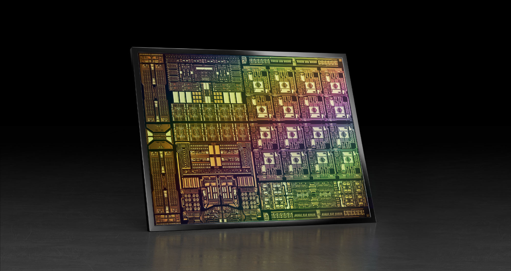
So says Michael Hochberg (pictured), who has been behind four start-ups including Luxtera and Elenion whose products used the technology. Hochberg has also co-authored a book along with Lukas Chrostowski on silicon photonics design.
In the first phase of silicon photonics, from 2000 to 2010, people wondered whether they could even do a design using the technology.
“Almost everything that was being done had to fit into an existing socket that could be served by some other material system,” says Hochberg.
A decade later it was more the case that sockets couldn’t be served without using silicon photonics. “Silicon photonics had dominated every one of the transceiver verticals that matter: intra data centre, data centre interconnect, metro and long haul,” he says.
Now people have started betting their systems using silicon photonics, says Hochberg, citing the examples as lidar, quantum optics, co-packaged optics and biosensing.
Several months ago Hochberg joined as president of Luminous Computing, a start-up that recently came out of stealth mode after raising $105 million in Series A funding.
Luminous is betting its future on silicon photonics as an enabler for an artificial intelligence (AI) supercomputer that it believes will significantly outperform existing platforms.
Machine learning
The vision of AI is to take tasks that were the exclusively the domain of the human mind and automate them at scale, says Hochberg.
Just in the last decade, the AI community has advanced from doing things using machine learning (ML) that are trivial for humans to tasks that only the most talented experts can achieve.
“We have reached the point where machine learning capabilities are superhuman in many respects,” says Hochberg. “Where they produce results quantifiably better than humans can.”
But achieving such machine learning progress has required huge amounts of data and hardware.
“The training runs for the state-of-the-art recommendation engines and natural language models take tens to hundreds of thousands of GPUs (graphics processing units) and they run from months to years,” says Hochberg.
Moreover, the computational demands associated with machine learning training aren’t just doubling every 18 months, like with Moore’s law, but every 3-4 months. “And for memory demands, it is even faster,” he says.
What that means is that the upper limit for doing such training runs are complete data centres.
Luminous Computing wants to develop AI hardware that scales quickly and simply. And a key element of that will be to use silicon photonics to interconnect the hardware.
“One of the central challenges scaling up big clusters is that you have one kind of bus between your CPU and memory, another between your CPU and GPU, another between the GPUs in a box and yet another – Infiniband – between the boxes,” says Hochberg.
These layers of connectivity run at different speeds and latencies that complicate programming for scale. Such systems also result in expensive hardware like GPUs being under-utilised.
“What we are doing is throwing massive optical interconnect at this problem and we are building the system around this optical interconnect,” says Hochberg.
Using sufficient interconnect will enable the computation to scale and will simplify the software. “It is going to be simple to use our system because if you need anything in memory, you just go and get it because there is bandwidth to spare.”
Supercomputing approach
Luminous is not ready to reveal its supercomputer architecture. But the company says it is vertically integrated and is designing the complete system including the processing and interconnect.
When the company started in 2018, it planned to use a photonic processor as the basis of the compute but the class of problems it could solve were deemed insufficiently impactful.
The company then switched to developing a set of ASICs designed around the capabilities of the optics. And it is the optics that rearchitects how data moves within the supercomputer.
“That is the place where you get order-of-magnitude advantages,” says Hochberg.
The architecture will tackle a variety of AI tasks typically undertaken by hyperscalars. “If we can enable them to run models that are bigger than what can be run today while using much smaller programming teams, that has enormous economic impact,” he says.
Hochberg also points out that many organisations want to use machine learning for lots of markets: “They would love to have the ability to train on very large data sets but they don’t have a big distributed systems engineering team to figure out how to scale things up onto big-scale GPUs; that is a market that we want to help.”
The possible customers of Luminous’s system are so keen to access such technology that they are helping Luminous. “That is something I didn’t experience in the optical transceiver world,” quips Hochberg.
The supercomputer will be modular, says Luminous, but its smallest module will have much greater processing capability than, say, a platform hosting 8 or 16 GPUs.
Silicon photonics
Luminous is confident in using silicon photonics to realise its system even though the design will advance how the technology has been used till now.
“You are always making a bet in this space that you can do something that is more complex than anything anyone else is doing because you are going to ship your product a couple of years hence,” says Hochberg
Luminous is has confidence because of the experience of its design team, the design tools it has developed and its understanding of advanced manufacturing processes.
“We have people that know how to stand up complex things,” says Hochberg.
Status
Luminous’s staff is currently around 100, a doubling in the last year. And it is set to double again by year-end.
The company is busy doing modelling work as to how the machine learning algorithms will run on its system. “Not just today’s models but also tomorrow’s models,” says Hochberg.
Meanwhile, there is a huge amount of work to be done to deliver the first hardware by 2024.
“We have a bunch of big complex chips we have to build, we have software that has to live on top of it, and it all has to come together and work,” concludes Hochberg.
Can a think tank tackle telecoms innovation deficit?
The Telecom Ecosystem Group (TEG) will publish shortly its final paper that concludes two years of industry discussion on ways to spur innovation in telecommunications.
The paper, entitled Addressing the Telecom Innovation Deficit, says telcos have lost much of their influence in shaping the technologies on which they depend.
“They have become ageing monocultures; disruptive innovators have left the industry and innovation is outsourced,” says the report.
The TEG has held three colloquiums and numerous discussion groups soliciting views from experienced individuals across the industry during the two years.
The latest paper names eight authors but many more contributed to the document and its recommendations.
Network transformation
Don Clarke, formerly of BT and CableLabs, is one of the authors of the latest paper. He also co-authored ETSI’s Network Functions Virtualisation (NFV) paper that kickstarted the telcos’ network transformation strategies of the last decade.
Many of the changes sought in the original NFV paper have come to pass.
Networking functions now run as software and no longer require custom platforms. To do that, the operators have embraced open interfaces that allow disaggregated designs to tackle vendor lock-in. The telcos have also adopted open-source software practices and spurred the development of white boxes to expand equipment choice.
Yet the TEG paper laments the industry’s continued reliance on large vendors while smaller telecom vendors – seen as vital to generate much-needed competition and innovation – struggle to get a look-in.
The telecom ecosystem
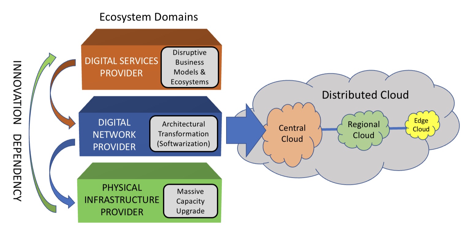
The TEG segments the telecommunications ecosystem into three domains (see diagram).
The large-scale data centre players are the digital services providers (top layer). In this domain, innovation and competition are greatest.
The digital network provider domain (middle layer) is served by a variety of players, notably the cloud providers, while it is the telcos that dominate the physical infrastructure provider domain.
At this bottom layer, competition is low and overall investment in infrastructure is inadequate. A third of the world’s population still has no access to the internet, notes the report.
The telcos should also be exploiting the synergies between the domains, says the TEG, yet struggle to do so. But more than that, the telcos can be a barrier.
Clarke cites the emerging metaverse that will support immersive virtual worlds as an example.
Metaverse
The “Metaverse” is a concept being promoted by the likes of Meta and Microsoft and has been picked up by the telcos, as evident at this week’s MWC Barcelona 22 show.
Meta’s Mark Zuckerberg recently encouraged his staff to focus on long-term thinking as the company transitions to become a metaverse player. “We should take on the challenges that will be the most impactful, even if the full results won’t be seen for years,” he said.
Telcos should be thinking about how to create a network that enables the metaverse, given the data for rendering metaverse environments will come through the telecom network, says Clarke.

“The real innovation will come when you try and understand the needs of the metaverse in terms of networking, and then you get into the telco game,” he says.
Any concentration of metaverse users will generate a data demand likely to exhaust the network capacity available.
“Telcos will say, ‘We aren’t upgrading capacity because we are not getting a return,’ and then metaverse innovation will be slowed down,” says Clarke.
He says much of the innovation needed for the metaverse will be in the network and telcos need to understand the opportunities for them. “The key is what role will the telcos have, not in dollars but network capability, then you start to see where the innovation needs to be done.”
The challenge is that the telcos can’t see beyond their immediate operational challenges, says Clarke: “Anything new creates more operational challenges and therefore needs to be rejected because they don’t have the resources to do anything meaningful.”
He stresses he is full of admiration for telcos’ operations staff: “They know their game.” But in an environment where operational challenges are avoided, innovation is less important.
TEG’s action plan
TEG’s report lists direct actions telcos can take regarding innovation. These cover funding, innovation processes, procurement and increasing competition.
Many of the proposals are designed to help smaller vendors overcome the challenges they face in telecoms. TEG views small vendors and start-ups as vital for the industry to increase competition and innovation.
Under the funding category, TEG wants telcos to allocate a least 5 per cent of procurement to start-ups and small vendors. The group also calls for investment funds to be set up that back infrastructure and middleware vendors, not just over-the-top start-ups.
For innovation, it wants greater disaggregation so as to steer away from monolithic solutions. The group also wants commitments to fast lab-to-field trials (a year) and shorter deployment cycles (two years maximum) of new technologies.
Competition will require a rethink regarding small vendors. At present, all the advantages are with the large vendors. It lists six measures how telcos can help small vendors win business, one being to stop forcing them to partner with large vendors. The TEG wants telcos to ensure enough personnel that small vendors get all the “airtime” they need with the telcos.
Lastly, concerning procurement, telcos can do much more.
One suggestion is to stop sending small vendors large, complex request for proposals (RFPs) that they must respond to in short timescales; small vendors can’t compete with the large RFP teams available to the large vendors.
Also, telcos should stop their harsh negotiating terms such as a 30 per cent additional discount. Such demands can hobble a small vendor.
Innovation
“Innovation comes from left field and if you try to direct it with a telco mindset, you miss it,” says Clarke. “Telcos think they know what ‘good’ looks like when it comes to innovation, but they don’t because they come at it from a monoculture mindset.”
He said that in the TEG discussions, the idea of incubators for start-ups was mentioned. “We have all done incubators,” he says. But success has been limited for the reasons cited above.
He also laments the lack of visionaries in the telecom industry.
A monoculture organisation rejects such individuals. “Telcos don’t like visionaries because culturally they are annoying and they make their life harder,” he says. “Disruptors have left the industry.”
Prospects
The authors are realistic.
Even if their report is taken seriously, they note any change will take time. They also do not expect the industry to be able to effect change without help. The TEG wants government and regulator involvement if the long-term prospects of a crucial industry are to be ensured.
The key is to create an environment that nurtures innovation and here telcos could work collectively to make that happen.
“No telco has it all, but individual ones have strengths,” says Clarke. “If you could somehow combine the strengths of the particular telcos and create such an environment, things will emerge.”
The trick is diversity – get people from different domains together to make judgements as to what promising innovation looks like.
“Bring together the best people and marvelous things happen when you give them a few beers and tell them to solve a problem impacting all of them,” says Clarke. “How can we make that happen?”

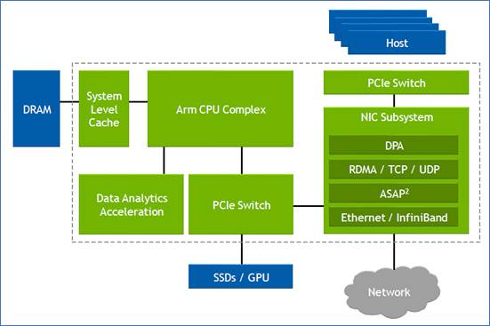
Nvidia's plans for the data processor unit
When Nvidia’s CEO, Jensen Huang, discussed its latest 400-gigabit BlueField-3 data processing unit (DPU) at the company’s 2021 GTC event, he also detailed its successor.
Companies rarely discuss chip specifications two generations ahead; the BlueField-3 only begins sampling next quarter.
The BlueField-4 will advance Nvidia’s DPU family.
It will double again the traffic throughput to 800 gigabits-per-second (Gbps) and almost quadruple the BlueField-3’s integer processing performance.
But one metric cited stood out. The BlueField-4 will increase by nearly 1000x the number of terabit operators-per-second (TOPS) performed: 1,000 TOPS compared to the BlueField-3’s 1.5 TOPS.
Huang said artificial intelligence (AI) technologies will be added to the BlueField-4, implying that the massively parallel hardware used for Nvidia’s graphics processor units (GPUs) are to be grafted onto its next-but-one DPU.
Why add AI acceleration? And will it change the DPU, a relatively new processor class?
Data processor units
Nvidia defines the DPU as a programmable device for networking.
The chip combines general-purpose processing – multiple RISC cores used for control-plane tasks and programmed in a high-level language – with accelerator units tailored for packet-processing data-plane tasks.
“The accelerators perform functions for software-defined networking, software-defined storage and software-defined security,” says Kevin Deierling, senior vice president of networking at Nvidia.
The DPU can be added to a Smart Network Interface Card (SmartNIC) that complements the server’s CPU, taking over the data-intensive tasks that would otherwise burden the server’s most valuable resource.
Other customers use the DPU as a standalone device. “There is no CPU in their systems,” says Deierling.
Storage platforms is one such example, what Deierling describes as a narrowly-defined workload. “They don’t need a CPU and all its cores, what they need is the acceleration capabilities built into the DPU, and a relatively small amount of compute to perform the control-path operations,” says Deierling.
Since the DPU is the server’s networking gateway, it supports PCI Express (PCIe). The PCIe bus interfaces to the host CPU, to accelerators such as GPUs, and supports NVMe storage. NVMe is a non-volatile memory host controller interface specification.
BlueField 3
When announced in 2021, the 22-billion transistor BlueField-3 chip was scheduled to sample this quarter. “We need to get the silicon back and do some testing and validation before we are sampling,” says Deierling.
The device is a scaled-up version of the BlueField-2: it doubles the throughput to 400Gbps and includes more CPU cores: 16 Cortex-A78 64-bit ARM cores.
Nvidia deliberately chose not to use more powerful ARM cores. “The ARM is important, there is no doubt about it, and there are newer classes of ARM,” says Deierling. “We looked at the power and the performance benefits you’d get by moving to one of the newer classes and it doesn’t buy us what we need.”
The BlueField-3 has the equivalent processing performance of 300 X86 CPU cores, says Nvidia, but this is due mainly to the accelerator units, not the ARM cores.
The BlueField-3 input-output [I/O] includes Nvidia’s ConnectX-7 networking unit that supports 400 Gigabit Ethernet (GbE) which can be split over 1, 2 or 4 ports. The DPU also doubles the InfiniBand interface compared to the BlueField-2, either a single 400Gbps (NDR) port or two 200Gbps (HDR) ports. There are also 32 lanes of PCI Express 5.0, each lane supporting 32 giga-transfers-per-second (GT/s) in each direction.
The memory interface is two DDR5 channels, doubling both the memory performance and the channel count of the BlueField-2.
The data path accelerator (DPA) of the BlueField-3 comprises 16 cores, each supporting 16 instruction threads. Typically, when a packet arrives, it is decrypted and the headers are inspected after which the accelerators are used. The threads are used if the specific function needed is not accelerated. Then, a packet is assigned to a thread and processed.
“The DPA is a specialised part of our acceleration core that is highlighly programmable,” says Deierling.
Other programmable logic blocks include the accelerated switching and packet processing (ASAP2) engine that parses packets. It inspects packet fields looking for a match that tells it what to do, such as dropping the packet or rewriting its header.
In-line acceleration
The BlueField-3 implements the important task of security.
A packet can have many fields and encapsulations. For example, the fields can include a TCP header, quality of service, a destination IP and an IP header. These can be encapsulated into an overlay such as VXLAN and further encapsulated into a UDP packet before being wrapped in an outer IP datagram that is encrypted and sent over the network. Then, only the IPSec header is exposed; the remaining fields are encrypted.
Deierling says the BlueField-3 does the packet encryption and decryption in-line.
For example, the DPU uses the in-line IPsec decode to expose the headers of the various virtual network interfaces – the overlays – of a received packet. Picking the required overlay, the packet is sent to a set of service-function chainings that use all the accelerators available such as tackling distributed denial-of-service and implementing a firewall and load balancing.
“You can do storage, you can do an overlay, receive-side scaling [RSS], checksums,” says Deierling. “All the accelerations built into the DPU become available.”
Without in-line processing, the received packet goes through a NIC and into the memory of the host CPU. There, it is encrypted and hence opaque; the packet’s fields can’t benefit from the various acceleration techniques. “It is already in memory when it is decrypted,” says Deierling.
Often, with the DPU, the received packet is decrypted and passed to the host CPU where the full packet is visible. Then, once the host application has processed the data, the data and packet may be encrypted again before being sent on.
“In a ‘zero-trust’ environment, there may be a requirement to re-encrypt the data before sending it onto the next hop,” says Deierling. “In this case, we just reverse the pipeline.”
An example is confidential healthcare information where data needs to be encrypted before being sent and stored.
DPU evolution
There are many application set to benefit from DPU hardware. These cover the many segments Nvidia is addressing including AI, virtual worlds, robotics, self-driving cars, 5G and healthcare.
All need networking, storage and security. “Those are the three things we do but it is software-defined and hardware-accelerated,” says Deierling.
Nvidia has an ambitious target of launching a new DPU every 18 months. That suggests the BlueField-4 could sample as early as the end of 2023.
The 800-gigabit Bluefield-4 will have 64-billion transistors and nearly quadruple the integer processing performance of the BlueField-3: from 42 to 160 SPECint.
Nvidia says its DPUs, including the BlueField-4, are evolutionary in how they scale the ARM cores, accelerators and throughput. However, the AI acceleration hardware added to the BlueField-4 will change the nature of the DPU.
“What is truly salient is that [1,000] TOPS number,” says Deierling. “And that is an AI acceleration; that is leveraging capabilities Nvidia has on the GPU side.”
Self-driving cars, 5G and robotics
An AI-assisted DPU will support such tasks as video analytics, 5G and robotics.
For self-driving cars, the DPU will reside in the data centre, not in the car. But that too will change.“Frankly, the car is becoming a data centre,” notes Deierling.
Deep learning currently takes place in the data centre but as the automotive industry adopts Ethernet, a car’s sensors – lidar, radar and cameras – will send massive amounts of data which an IC must comprehend.
This is relevant not just for automotive but all applications where data from multiple sensors needs to be understood.
Deierling describes Nvidia as an AI-on-5G company.
“We have a ton of different things that we are doing and for that, you need a ton of parallel-processing capabilities,” he says. This is why the BlueField-4 is massively expanding its TOPS rating.
He describes how a robot on an automated factory floor will eventually understand its human colleagues.
“It is going to recognize you as a human being,“ says Deierling. “You are going to tell it: ‘Hey, stand back, I’m coming in to look at this thing’, and the robot will need to respond in real-time.”
Video analytics, voice processing, and natural language processing are all needed while the device will also be running a 5G interface. Here, the DPU will reside in a small mobile box: the robot.
“Our view of 5G is thus more comprehensive than just a fast pipe that you can use with a virtual RAN [radio access network] and Open RAN,” says Deierling. “We are looking at integrating this [BlueField-4] into higher-level platforms.”

Huawei sets transmission record with new modulator

Coherent discourse: Part 1
A paper from Huawei and Sun Yat-Sen University in the January issue of the Optica journal describes a thin-film lithium niobate modulator. The modulator enabled a world-record coherent optical transmission, sending nearly 2 terabits of data over a single wavelength.
Much of the industry’s focus in recent years has been to fit coherent optical technology within a pluggable module.
Such pluggables allow 400-gigabit coherent interfaces to be added to IP routers and switches, serving the needs of the data centre operators and telecom operators.
But research labs of the leading optical transport vendors continue to advance high-end coherent systems beyond 800-gigabit-per-wavelength transmissions.
Optical transport systems from Ciena, Infinera and Huawei can send 800-gigabit wavelengths using a symbol rate of 96-100 gigabaud (GBd).
Acacia Communications, part of Cisco, detailed late last year the first 1.2-terabit single-wavelength coherent pluggable transceiver that will operate at 140GBd, twice the symbol rate of 400-gigabit modules such as 400ZR.
Now Huawei has demonstrated in the lab a thin-film lithium niobate modulator that supports a symbol rate of 220GBd and beyond.
Maxim Kuschnerov, director of the optical and quantum communications laboratory at Huawei, says the modulator has a 110GHz 3dB bandwidth but that it can be operated at higher frequencies, suggesting a symbol rate as high as 240GBd.
Thin-film lithium niobate modulator
Huawei says research is taking place into new materials besides the established materials of indium phosphide and silicon photonics. “It is a very exciting topic lately,” says Kuschnerov.
He views the demonstrated thin-film lithium niobate optical modulator as disruptive: “It can cover up several deficiencies of today’s modulators.”
Besides the substantial increase in bandwidth – the objective of any new coherent technology – the modulator has performance metrics that benefit the coherent system such as a low driving voltage and low insertion loss.
A driving voltage of a modulator is a key performance parameter. For the modulator, it is sub-1V.
The signal driving the modulator comes from a digital-to-analogue (D/A) converter, part of the coherent digital signal processor (DSP). The D/A output is fed into a modulator driver. “That [driver] requires power, footprint, and increases the complexity of integrating the [modem’s] modules tighter,” says Kuschnerov.
The modulator’s sub-1V drive voltage is sufficiently small that the DSP’s CMOS-based D/A can drive it directly, removing the modulator driver circuit that also has bandwidth performance limitations. The modulator thus reduces the transmitter’s overall cost.
The low-loss modulator also improves the overall optical link budget. And for certain applications, it could even make the difference as to whether optical amplification is needed.
“The modulator checks the box of very high bandwidth,” says Kuschnerov. “And it helps by not having to add a semiconductor optical amplifier for some applications, nor needing a driver amplifier.”
One issue with the thin-film modulator is its relative size. While not large – it has a length of 23.5mm – it is larger than indium phosphide and silicon photonics modulators.
1.96-terabit wavelength
Huawei’s lab set-up used a transmit coherent DSP with D/As operating at 130 Giga-samples-per-second (GS/s) to drive the modulator. The modulation used was a 400-quadrature amplitude modulation (400-QAM) constellation coupled with probabilistic constellation shaping.
A 10 per cent forward error correction scheme was used such that, overall, 1.96-terabits per second of data was sent using a single wavelength.
The D/A converter was implemented in silicon germanium using high-end lab equipment to generate the signal at 130GS/s.
“This experiment shows how much we still need to go,” says Kuschnerov. “What we have done at 130GBd shows there is a clear limitation with the D/A [compared to the 220GBd modulator].”
Baud-rate benefits
Increasing the baud rate of systems is not the only approach but is the favoured implementation choice.
What customers want is more capacity and reducing the cost per bit for the same power consumption. Increasing the baud rate decreases the cost and power consumption of the optical transceiver.
By doubling the baud rate, an optical transceiver delivers twice the capacity for a given modulation scheme. The cost per bit of the transceiver decreases as does the power consumed per bit. Instead of two transceivers and two sets of components, one transceiver and one set are used instead.
But doubling the baud rate doesn’t improve the optical system’s spectral efficiency since doubling the baud rate doubles the channel width. That said, algorithmic enhancements are added to each new generation of coherent modem but technically, the spectral efficiency practically no longer improves.
Huawei acknowledges that while the modulator promises many benefits, all the coherent modem’s components – the coherent ASIC, the D/A and analogue-to-digital (D/A) converters, the optics, and the analogue circuitry – must equally scale. This represents a significant challenge.
Kuschnerov says optical research is finding disruptive answers but scaling performance, especially on the electrical side, remains a critical issue. “How do you increase the D/A sampling rates to match these kinds of modulator technologies?” he says. “It is not straightforward.”
The same is true for the other electrical components: the driver technologies and the trans-impedance amplifier circuits at the receiver.
Another issue is combining the electrical and optical components into a working system. Doubling the signalling of today’s optical systems is a huge radio frequency design and packaging challenge.
But the industry consensus is that with newer CMOS processes and development in components and materials, doubling the symbol rate again to 240GB will be possible.
But companies don’t know – at least they are not saying – what the upper symbol rate limit will be. The consensus is that increasing the baud rate will end. Then, other approaches will be pursued.
Kuschnerov notes that if a 1.6-terabit transceiver could be implemented using a single wavelength or with eight 200Gbps ones with the same spectral performance, cost, footprint and power consumption, end users wouldn’t care which of the two were used.
However, does optics enable such greater parallelism?
Kuschnerov says that while decades of investment has gone into silicon photonics, it is still not there yet.
“It doesn’t have the cost-effectiveness at 16, 32 or 64 lanes because the yield goes down significantly,” he says. “We as an industry can’t do it yet.”
He is confident that, soon enough, the industry will figure out how to scale the optics: “With each generation, we are getting better at it.”
Coherent engineers will then have more design options to meet the system objectives.
And just like with microprocessors, it will no longer be upping the clock frequency but rather adopting parallel processing i.e. multiple cores. Except, in this case, it will be parallel coherent optics.

Evolving packet processing by a factor of 1000
Nokia’s FP5 IP router chipset has been a design four years in the making, the latest iteration of a two-decades-old packet processing architecture.
The 3-device FP5 chipset is implemented using a 7nm CMOS process. The design uses 2.5D stacked memory and is the first packet processor with 112 gigabit-per-second (Gbps) serialiser-deserialiser (serdes) interfaces. Also included are line-rate hardware encryption engines on the device’s ports.

Ken Kutzler
What hasn’t been revealed are such metrics as the chipset's power consumption, dimensions and transistor count.
Ken Kutzler, vice president of IP routing hardware at Nokia IP Networks Division, says comparing transistor counts of chips is like comparing software code: one programmer may write 10,000 lines while another may write 100 lines yet both may execute the same algorithm.
“It’s not always the biggest and baddest chip in the world that compares well,” says Kutzler.
GPU-CPU union
Kutzler says the FP5 can be characterised as combining the attributes of a graphics processing unit (GPU) with a general-purpose processor (CPU).
A GPU must deal with massive amounts of data - pixels - flowing through the device. “It’s a data flow model and that is what a packet processor has to do,” he says. A CPU, in contrast, processes data in blocks. A lot of the data processing involves moving data.
“You don't want to spend all that time with the processor moving data around, you want the data to move and the processing acting upon it,” says Kutzler. This is what the FP5 does: processes data as it flows.
“Our device has to be like a GPU in how data moves and like a CPU in that it has to be general-purpose,” he says. By general purpose, Nokia means having a programmable packet-processing pipeline rather than predefined hardware accelerator blocks.
“For service providers, the amount of features are pretty intense and they are ever-changing,” says Kutzler. “We have tended to forgo specialised engines that presuppose how something is parsed.”

Source: Nokia, Gazettabyte
Programmable pipelines
As implied by the name, the FP5 is the fifth-generation implementation of what started in 2003 as Alcatel’s FP packet processor. The FP had a 10Gbps line rate and used 30 packet-processing cores that ran microcode, each core being clocked at 190MHz.
The Alcatel-Lucent FP2 followed in 2007. The 100Gbps FP2 nearly quadrupled both the cores (112) and their clock rate (840MHz) and the trend continued with the 400Gbps FP3 announced in 2011.
The FP3 has 288, 1GHz cores arranged in a 2D array: 32 rows by 9 columns. Each row acts as a packet-processing pipeline that can be partitioned to perform independent tasks. The columns perform table look-ups and each column can be assigned more than one task.
The FP3 continues to carry IP network traffic and have its features enhanced using software upgrades, highlighting the benefit of a programmable packet processing architecture, says Kutzler.
The chipsets are also backwards compatible; the FP5 can implement the FP3’s instruction set, for example, but it also includes newer instructions. In one clock cycle, multiple instructions can be executed in an FP5 core. The core also supports multi-threading that did not exist with the FP3 whereby several instruction threads are interleaved and processed in parallel.
Chipset partitioning
Kutzler stresses that Nokia sells platforms and solutions, not chips. What matters to Nokia is that the silicon meets its platform requirements.
“I don’t really care what the ASIC speed is because I’m not going to sell it,” says Kutzler. “I care what the board speeds want.” For FP5-enabled platforms, that is 14.4 terabits.
But some customers want 2.4-terabit and 4.8-terabit capacities so what is needed is a power-efficient cost-effective solution across designs.
Partitioning the chipset functionality is reconsidered with each generation of design. “We will move things where it makes the most sense when designing our entire solution,” says Kutzler.
The 16nm CMOS 3Tbps FP4 chipset comprises a packet processor (p-chip) and the traffic manager (q-chip) as well as what was then a new chip, the e-chip. A media access controller (MAC), the e-chip parcels data from the router’s client-side pluggable optical modules for the packet processor.
However, Nokia combined the s-chip and t-chip withe FP4; the s-chip is a switch IC while the t-chip interfaces to the router’s fabric.
With the 7nm CMOS FP5, the p-chip and q-chip have finally been combined along with the t-chip.
Kutzler says the p- and q-chips could have been combined with earlier generation designs. But given the die cost (yield), it was deemed better to keep them separate. This also has system advantages: some FP3-based systems were configured using a combination of two p-chips and one q-chip.
“The p-chip is malleable; you can put it serially or in parallel,” says Kutzler. The compiler is told how the design is set up and the microcode is compiled accordingly.
The latest partitioning means the FP5 is a three-device chipset: the main chip (the packet processor, traffic manager and fabric interface), s-chip and the e-chip.
Terabit scale
The FP4 required a significant redesign for the architecture to continue to scale that took six years rather than its typical four-year design cycle.
“These were low-level changes, it [the FP4] still runs the same microcode but enhanced in such a way that the architecture can evolve,” says Kutzler.
The FP4 uses 1,040 cores, each enhanced to execute two instructions per clock cycle. The die-shrink allowed the cores to be clocked at 1.5GHz and hyper-threading was added, as mentioned. The FP4 also adopted 56Gbps serdes technology from Broadcom.
“When we talked about the FP4, we said it is setting this up for FP5 and that the FP5 would be coming much faster,” says Kutzler.
The FP5 increases the core count to 1,248 and doubles the serdes speed to 112Gbps.
“Serdes consume a considerable amount of power,” says Kutzler. Yet doubling the serdes speed saves power overall; a 112Gbps serdes consumes more power than a 56Gbps one but much less than twice the power.
Equally, putting two devices (the p-chip and q-chip) into one chip saves power otherwise required for chip-to-chip communications. Power is also saved when certain device features are not in use.
Nokia claims the FP5 design consumes a quarter of the power of the FP4 ones when measured in Watts-per-gigabit (0.1W/gigabit compared to 0.4W/gigabit).
The 0.1W/gigabit is with the chipset’s features turned on including the encryption engines. “If a limited feature set is required, our expected power numbers will be below the full-featured typical power consumption number,” says Jeff Jakab, Nokia’s director of IP routing hardware.
Memory
One issue IP router chip designers face is that the line rates of their chips are rising far faster than memory access speeds.
There are two memory types used for routing, each with its own requirements, says Nokia.
The first memory type is used for counters and table look-ups while the second buffers packets.
For counters/ look-ups what is needed is very high-speed memory that supports 32-bit and 64-bit reads and writes. In contrast, buffering requires much larger memories; the packet blocks are much larger requiring bigger reads and writes but they are not as simultaneous, says Kutzler.
Nokia developed its own ‘smart memory’ for the FP4 that is command-line driven. This means that a command can be used to perform a task that otherwise would require multiple memory accesses, thereby adding much-needed parallelism.
Four such smart memory dies are included in the FP4’s p-chip while for buffering, four high-bandwidth memory (HBM) blocks, each comprising stacked memory die, are part of the q-chip.
The FP5 integrates the smart memory on-chip, freeing up room for the latest HBM2e technology. “This allows us to get the speeds we need,” says Kutzler. “So when we say we have a 14.4-terabit card, it allows true QoS (quality of service) on every packet.”
“All chipsets released prior to the FP5 make use of HBM2 and are constrained to a maximum of some 1.7 terabits of full-duplex bandwidth to buffer memory,” says Jakab.
The FP4's HBM2 buffer memory supports a 1.5-terabit line rate whereas HBM2e can support a 2.4-terabit line rate.
“We are not aware of any other chipsets on the market that make use of HBM2e,” says Jakab, adding that these memory types generally cannot be substituted one for another without considerable redesign effort.
Nokia’s use of memory includes the FP5’s e-chip which plays a key role, as is now explained.
Board considerations
The e-chip is deliberately separated from the main chip as it performs packet pre-processing and packet pre-classification as well as pre-buffering in front of the packet processor.
“We use multiple e-chips in front of our packet processor to allow the faceplate of our card to expand in terms of port capabilities beyond the forwarding limit of our packet processor,” says Jakab.

Jeff Jakab
The e-chip delivers two advantages. It does away with pre-aggregation boxes in front of Nokia’s 7750 SR platform. Such 1 rack unit (1RU) pre-aggregation boxes are used to groom traffic into an edge router or smart aggregation platform.
A typical pre-aggregation box supports 32MB of buffering, says Jakab, whereas each e-chip uses nearly 20x that amount.
“It [using the e-chip] collapses the platforms in front, saving power and rack space while eliminating a layer from the network,” says Jakab.
In many IP edge or core applications, customers are not capacity restricted but port restricted. They run out of ports long before they run out of capacity because the majority of flows are all fractional.
A fractional flow is one that does not fill up the full bandwidth of an interface, for example 50 gigabits of traffic on a 100-gigabit interface or 7 gigabits of traffic on a 10 Gigabit Eternet interface.
This is the design use case of Nokia’s SR-1 router platform. “Aggregating a ton of fractional flows with many many connectivity option types is the ideal use case for smart aggregation," says Jakab.
The e-chip also helps Nokia's systems to benefit from what it calls intelligent aggregation which uses pre-classification and pre-buffering to guarantee the flows that matter most.
“It goes well beyond basic oversubscription because we pre-buffer and pre-classify to ensure that high priority traffic is always guaranteed,” says Jakab.
This is different from classic oversubscription where, when the given rate for a packet processor is exceeded, the next packet is by default discarded, irrespective of QoS, says Jakab.
“It means we can flexibly offer more ports on the faceplate of a card to satisfy increasing port requirements without fear of indiscriminate packet drops,” he says.
Nokia points out that its FP5 line cards expand capacity by 3x.
Its 4.8Tbps expandable media adaptor (XMA) card supports 12 terabit of intelligent aggregation by using four FP4 chipsets. Its latest XMA is 14.4Tbps, supports 19.2Tbps of IA, and uses six FP5 chipsets.
What next
Extrapolating four years hence to 2025, the FP6 packet processor will likely be a 5nm or 3nm CMOS design with a packet-processing capacity of some 10Tbps, a 1000x improvement on the first FP.
Kutzler stresses that the speed of the device is less important than meeting its IP system requirements for the decade that will follow. It is these requirements that will shape the FP6 design.
Kutzler did share one thing about the FP6: it will use 224Gbps serdes.