
Will AI spur revenue growth for the telcos?
- A global AI survey sponsored by Ciena highlights industry optimism
- The telcos have unique networking assets that can serve users of AI.
- Much is still to play out and telcos have a history of missed opportunities.
The leading communications service providers have been on a decade-long journey to transform their networks and grow their revenues.
To the list of technologies the operators have been embracing can now be added artificial intelligence (AI).
AI is a powerful tool for improving their business efficiency. The technology is also a revenue opportunity and service providers are studying how AI traffic will impact their networks.
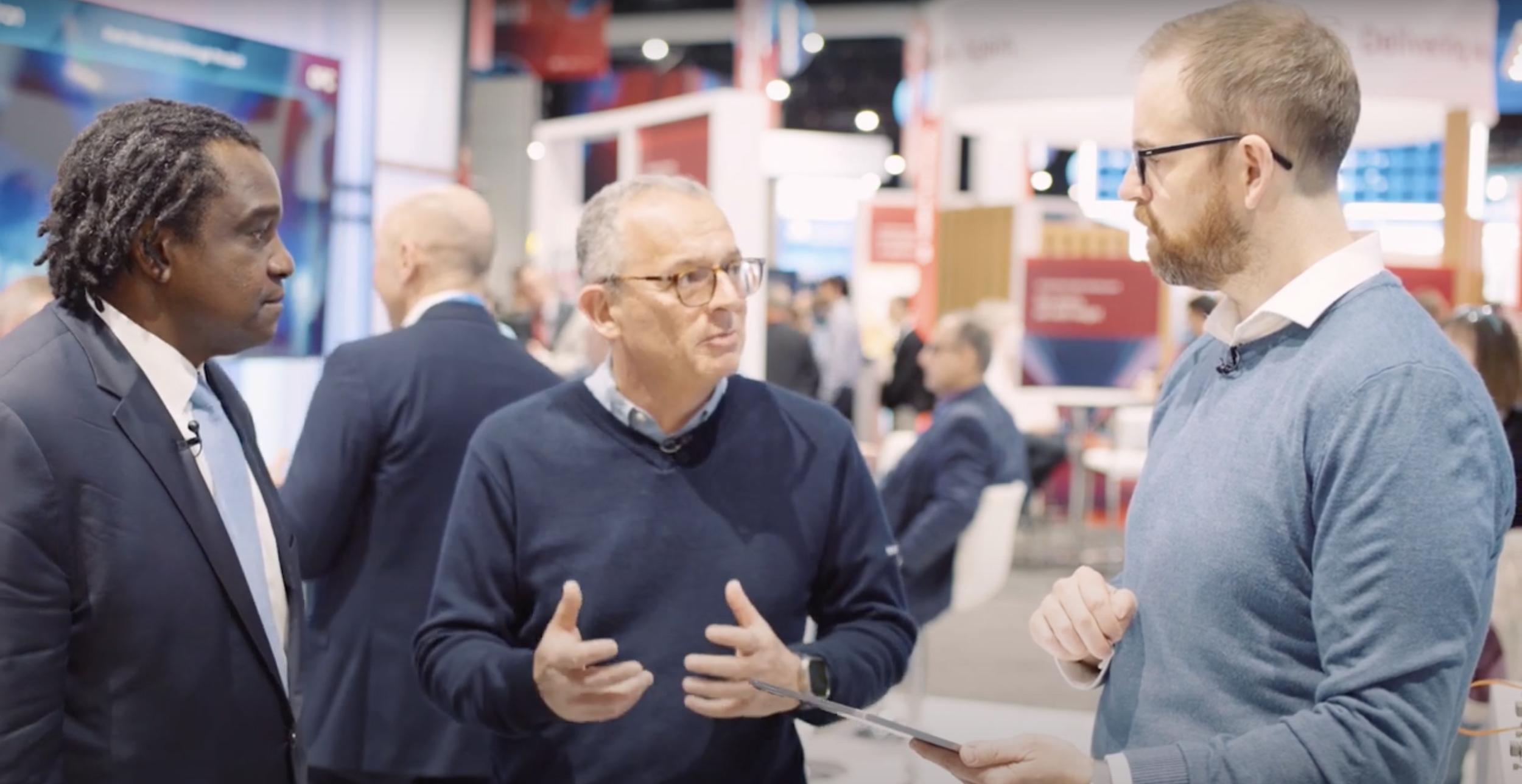
“This is the single biggest question that everyone in this industry is struggling with,” says Jürgen Hatheier. “How can the service providers exploit the technology to grow revenues?”
However, some question whether AI will be an telecom opportunity.
“The current hype around AI has very little to do with telcos and is focused on hyperscalers and specifically the intra-data centre traffic driven by AI model training,” says Sterling Perrin, senior principal analyst at HeavyReading. “There is a lot of speculation that, ultimately, this traffic will spread beyond the data centre to data centre interconnect (DCI) applications. But there are too many unknowns right now.”
AI survey
Hatheier is chief technology officer, international at Ciena. He oversees 30 staff, spanning Dublin to New Zealand, that work with the operators to understand their mid- to long-term goals.
Ciena recently undertook a global survey (see note 1, bottom) about AI, similar to one it conducted two years ago that looked at the Metaverse.
Conducting such surveys complements Ciena’s direct research with the service providers. However, there is only so much time a telco’s chief strategy officer (CSO) or chief technology officer (CTO) can spend with a vendor discussing strategy, vision, and industry trends.
“The survey helps confirm what we are hearing from a smaller set,” says Hatheier.
Surveys also uncover industry and regional nuances. Hatheier cites how sometimes it is the tier-two communications service providers are the trailblazers.
Lastly, telcos have their own pace. “It takes time to implement new services and change the underlying network architecture,” says Hatheier. “So it is good to plan.”

Findings
The sectors expected to generate the most AI traffic are financial services (46 per cent of those surveyed), media and entertainment (43 per cent), and manufacturing (38 per cent). Hatheier says these industries have already been using the technology for a while, so AI is not new to them.
Sterling Perrin
For financial services, an everyday use of AI is for security, detecting fraudulent transactions and monitoring video streams to detect anomalous behavior at a site. The amount of traffic AI applications generate can vary greatly. This is common, says Hatheier; it is the use that matters here, not the industry.
“I would not break it down by the industries to say, okay, this industry is going to create more traffic than another,” says Hatheier. “For financial services, if it is transaction data, it’s a few lines of text, but if it is video for branch security, the data volumes are far more significant.”
AI is also set to change the media and entertainment sector, challenging the way content is consumed. Video streaming uses content delivery networks (CDNs) to store the most popular video content close to users. But AI promises to enable more personalised video, tailored for the end-user. Such content will make the traffic more dynamic.
Another example of personalised content is for marketing and advertising. Such personalisation tends to achieve better results, says Hatheier.
AI is also being applied in the manufacturing sector. Examples include automating supply-chain operations, predictive maintenance, and quality assurance.
Car manufacturers check a vehicle for any blemishes at the end of a production line. This usually takes several staff and lasts 10-15 minutes. Now with AI, the inspection can be completed as the cars passes by. “This is a potent application that could run on infrastructure within the manufacturing site but use a service provider’s compute assets and connectivity,” says Hatheier.
The example shows how AI produces productivity gains. However, AI also promises unique abilities that staff cannot match.

Traffic trends
If the history of telecoms is anything to go by, applications that drove traffic in the network rarely lead to revenue growth for the service providers. Hatheier cites streaming video, gaming, and augmented reality as examples.
However, the operators have assets at network edge and the metro that can benefit AI usage. They also have central offices that can act is distributed data centres for the metro and network edge.
Hatheier says users have an advantage if they consume AI applications across a fibre-based broadband network. But certain countries, such as Saudi Arabia and India, mainly use wireless for connectivity.
“AI applications will need to adapt to what is available, and if people want to consume low-latency applications, there is 5G slicing,” says Hatheier. “At the end of the day, there is no way around fibre.”
Optical networking
Government policy regarding AI and regulations to ensure data does not cross borders also play a part.
“It’s an important decision criterion, as we saw in the survey response,” says Hatheier. “So private AI and local computing will be an important decision factor.”
Another critical decision influencing where data centres are built is power. “We see all the gold rush in the Nordics right now with their renewable power and cool climates,” says Hatheier. “You don’t need to cool your servers as much, and it requires a lot of connectivity.”
However, as well as these region-specific data centre builds, there will also be builds in metropolitan areas using smaller distributed data centres.
“Let’s say there are 20 sizable edge or metro compute centres for AI, and you would need three or four to run a big training job,” says Hatheier. “You will not create a permanent end-to-end connection between them because sometimes there will not be four that need to work together, but five, seven, and 11.”
Such a metro network would require reconfigurable optical add-drop multiplexer (ROADM) technology to connect wavelengths between those clusters based on demand to keep sites busy, to avoid expensive AI clusters being idle.
These are opportunities for the CSPs. And while much is still to happen, such discussions are taking place between systems vendors and the telcos.
For Heavy Reading’s Perrin, the more telling opportunity is the telcos’ own use of AI rather than the networking opportunity.
“As a vertical industry, telecom is not typically a leading-edge adopter of any new technology due to many factors, including culture, size, legacy infrastructure and processes, and government regulations,” he says. “I don’t believe AI will be any different.”
Hatheier points to the survey’s finding of general optimism that sees AI as an opportunity rather than a challenge or business risk.
“We have seen very little differences between countries,” says Hatheier. “That may have to do with the fact that emerging countries get as much attention of data centre investment than more developed ones.”

Nokia picks Infinera to boost its optical networking arm
Nokia has announced its intention to buy optical networking specialist Infinera for $2.3 billion.

The motivation for the Infinera acquisition is scale, said Nokia CEO Pekka Lundmark, during an analyst call detailing the announcement.
Optical networking is how communications service providers and hyperscalers cope with the exponential traffic growth.
Continual innovation is required to reduce the cost and power consumed to transport such traffic. For a systems vendor, having scale helps meet these aims.
Optical networking wasn’t always central to Nokia’s strategy. In 2013, Nokia sold its optical networking arm to Marlin Equity Partners, which became Coriant.
Now, Nokia wants to be a leading optical networking vendor by acquiring Infinera, a company that bought Coriant in 2018.
Nokia’s announcement regarding Infinera comes days after it sold its submarine optical networking business. “It’s part of a larger refocusing on core strengths and higher-growth areas,” says John Lively, principal analyst at market research company LightCounting.
Market share and geographical balance
“We estimate that the combined entity will have a 20 per cent market share,” says Jimmy Yu, vice president at market research firm Dell’Oro Group.
Dell’Oro’s vendor ranking data for 2023 gave Huawei a 30 per cent market share, Nokia+Infinera would be second (20 per cent), while Ciena had a 19 per cent share.
Nokia would also strengthen its sales and balance its presence in key markets globally. Infinera has gained webscale customers in recent years, a significant and growing market compared to telecoms.

“Nokia has had competitive long-haul coherent optics in terms of performance but has failed to get much traction outside its traditional CSP markets,” says Lively. “The Infinera deal gives Nokia access to the faster-growing data centre market and a pluggable coherent product line with a strong order pipeline.”
Nokia says the optical networking deal will also strengthen its overall Network Infrastructure business unit that includes IP Networks and Fixed Networks.

Technologies
Nokia and Infinera offer optical networking systems based on high-end embedded coherent modems and coherent pluggable optical modules.
In 2020, Nokia bought Elenion Technologies, giving the company a silicon photonics coherent design team and a way to address the growing pluggable coherent module marketplace.
Early last year, Nokia announced its 1.2-terabit PSE-6s coherent modem for demanding optical transport applications. Two PSE-6s coherent modems can be used to create a 2.4-terabit line card. Nokia started shipping the modem in late 2023 and already has 15 customers.
Infinera is known for its expertise in indium phosphide photonic integrated circuits. The systems vendor’s latest embedded coherent modem is the 1.2-terabit ICE-7 and it offers a range of coherent pluggable products.
Infinera has recently announced design wins for 800-gigabit ZR/ ZR+ for the hyperscale market, and bidirectional 400G ICE-X pluggables for the cable segment. It valued both opportunities at several hundred million dollars, says LightCounting
Dell’Oro’s Yu says Nokia’s acquisition of Infinera would allow it to develop the entire optical front end in-house. He highlights Infinera’s development of indium phosphide, its indium phosphide chip fabrication plants, and the additional optical front-end components such as the trans-impedance amplifier (TIA), driver, and laser.
“The only other vendors with this much done in-house are Huawei and Ciena,” says Yu. “Cisco has all of this except for indium phosphide development.”
Infinera’s success with webscale companies includes optical networking gear for data centre interconnect. The company is also eyeing the optical networking opportunity inside the data centre which promises significant unit volumes. To this aim, the company is developing a range of ICE-D optical engines.
The company has not detailed much about ICE-D besides claiming that it offers power savings of up to 75 per cent. The power-saving claim is based on using a direct-drive approach and a highly integrated design – optics and electronics. Infinera will likely detail first ICE-D offerings at the ECOC show in September.
Once the acquisition is approved, Nokia will have its own lasers and complement its silicon photonics technology with indium phosphide design expertise. Nokia expects to speed up its coherent modem and product roadmap by combining the DSP design teams.
Challenges and Opportunities
Nokia and Infinera are already advanced in the design of their next-generation coherent designs—the PSE-7 and ICE-8, respectively. These are the two companies responses to Ciena’s 200-gigabaud WaveLogic 6 Extreme, which supports up to a 1.6-terabit optical wavelength.
Developing a coherent DSP in a 3nm or 2nm CMOS process is costly. Both companies will continue to develop their designs for now, given that the deal is expected to close in the first half of 2025. However, they will be keen to agree on what design to choose. This had happened before when Infinera halted what would have been the ICE-5 in favour of Coriant’s design and turned its full attention to developing the ICE-6.
The industry is challenged to keep driving down the cost-per-bit and power-per-bit. The preferred approach is to keep increasing the symbol rate even if the spectral efficiency gains are more modest with each generation due to Shannon’s limit being approached.
However, increasing the baud rate is increasingly challenging and will lead to new parallel designs. Pooling the two companies’ coherent design expertise will help here.
Nokia says another factor for the deal is the expected growth in AI traffic. Such AI traffic is on top of fixed and mobile traffic growth. AI will drive intra-data and inter-data centre networking in the core and edge. Such traffic will be for training and inferencing.
The rest
There will be a notable gap between the top 3 and the remaining optical vendors, who all have a single digital market share. However, the consensus is that the niche players will have a role. Since telecom equipment is a critical infrastructure, operators and governments must promote using local vendors when available. Yu cites the examples of the Padtecs in South America and Tejas in India.

Cloud and AI: Opportunities that must be grabbed
The founder of Cloud Light, Dennis Tong, talks about the company, how its sale to Lumentum came about, and the promise of cloud and AI markets for optics.

For Dennis Tong (pictured), Hong Kong is a unique place that has a perfect blend of the East and West.
Tong, the founder and CEO of optical module specialist Cloud Light, should know. The company is headquartered in Hong Kong and has R&D offices in Hong Kong and Taipei, Taiwan. Cloud Light also has manufacturing sites in Asia: in the Chinese city of Dongguan—two hours by car, north of Hong Kong—and in the Philippines.
Now, Cloud Light is part of Lumentum. The U.S. photonics firm bought the optical module maker for $750 million in November 2023.
Tie-up
Cloud Light is a volume manufacturer of optical modules. The company takes 12-inch silicon photonic wafers, tests the wafers’ dies, and packages them for use in optical modules.
Cloud Light has a long relationship with Lumentum, using the U.S. company’s continuous-wave lasers for its silicon photonic-based optical modules.
Tong says he has been in photonics for 30 years and has good friends at Lumentum. “We had opportunities to chat and exchange views as to where the industry is going, and we shared a common vision,” he says. Eventually, the talk turned to a possible merger and acquisition.
Tong says the decision to sell the company centred on how best to grow the company. Cloud Light would have continued to do well, he says, but the company could grow much faster if he and his 1,600 staff joined Lumentum.
It is also timely. “Opportunities such as cloud and AI, they don’t come along very often,” says Tong.

Wafer-in, Product-out
Cloud Light has developed a manufacturing process dubbed “wafer-in, product-out.”
Turning a photonic integrated circuit (PIC) into a packaged optical module involves many stages and players. Designers of a PIC pass it to a foundry that results in the wafer. The wafer is shipped to an outsourced semiconductor assembly and test (OSAT) that does wafer back-end tasks: testing and dicing the wafer, and polishing. The working PICs—the known good dies—are shipped to a contract manufacturer that makes the pluggable modules.
“You can see that the entire collaboration chain is fragmented,” says Tong. “With our wafer-in, product-out process, we put everything in one group.”
Cloud Light takes the wafer from the foundry and does all the steps resulting in the delivered module.
Tong says the advantage of undertaking the complete process includes improved product yield. For example, the company measures coupling loss to the PIC and its optical waveguide loss during testing, and uses the insight to improve product yield.
Cloud Light has developed its own equipment to support automation. This know-how means that its design staff can work with the process and equipment colleagues to tailor the manufacturing process for new product designs. The precise assembly of unique micro-optics is one example.
It is this expertise and capability that particularly interested Lumentum in Cloud Light.
According to Tong, accumulating expertise in the different production areas has taken years: “There is a lot of subtlety to it, and we started to set this up in 2017.”
Hyperscaler business
Cloud Light succeeded early with a hyperscaler, making a 4×10-gigabit multimode VCSEL-based transceiver. But it soon realised market growth was coming from single-mode optical transceivers.
Its decision to pursue its wafer-in, product-out strategy stemmed from a desire to avoid becoming one of many single-mode optical transceiver makers. “We didn’t think we would add any value to the market by just creating a me-too company,” says Tong.
If the company was going to invest in a new platform, it would have to be scalable to support high volumes.
“It was very clear that silicon photonics was the right thing to do,” says Tong. “We were one of the first, if not the first, to launch a 400-gigabit silicon photonics-based transceiver in 2019.”
Cloud Light pitched its in-house scalable manufacturing approach to a hyperscaler that liked its plan, resulting in the company securing the hyperscaler as a customer.
Plans
Since the acquisition’s completion, Lumentum has given Cloud Light broad scope; there is no rush for full-blown integration, says Tong.
“Our mandate is to continue to grow the module business,” he says. “And we are open to using components from Lumentum and other suppliers.”
Lumentum’s components also offer Cloud Light the ability to create new products. “Customers are seeing us as more equipped, which opens up new, interesting opportunities,” says Tong.
Moreover, Cloud Light is not solely making modules for Lumentum. “The reality is that this is a very dynamic market, dominated by a few customers,” says Tong. “We are open to different business models as long as we can add value.”
Opportunities
At the time of the deal, Lumentum revealed that it expected Cloud Light would add $200 million plus to its yearly income. Cloud Light’s $200 million in revenues in the previous year was almost all from 400-gigabit and higher-speed transceiver sales.
Lumentum also makes coherent optical modems, ROADMs, and 3D sensing for commercial applications. Tong says coherent modules are one obvious opportunity for Cloud Light: “If you look into the future, I think the line between cloud/ datacom and telecom will become blurred.”
Cloud and AI will drive volumes, and the silicon photonics platform will be applicable for coherent modems as well. “So, a lot of the things that we have developed will also be applicable to coherent modules in the future,” says Tong. “And it is definitely applicable if one day coherent optics makes its way into the data centre.”
Coherent optics modules will keep increasing symbol rate and use more sophisticated coding schemes, but at some point, the effective data rate per line will start to plateau. To increase bandwidth beyond that, designs will go parallel by adding more channels. “Adding more fibre or more wavelengths, then it comes back to density, and then it’s all about packaging,” says Tong.
The ability to change its automated assembly for new applications also suggests that Cloud Light’s manufacturing capability could benefit Lumentum’s other product lines, such as ROADMs and even new markets such as optical circuit switches.
Co-packaged optics
Co-packaged optics are seen as one solution for applications where standard pluggable optics are no longer suitable.
Tong says that there are still issues before co-packaged optics are deployed at scale. One challenge is reliability; hyperscalars will not deploy the technology at scale until it has demonstrable good quality and reliability.
“The emergence of AI and cloud may accelerate that deployment, simply because of the volumes they are using and the density issue,” says Tong. Cost and thermal issues is also something co-packaged optics can address.
Cloud Light is ready for the advent of co-packaged optics. For its 800-gigabit transceiver, it can package a bare-die digital signal processor right next to the silicon photonics optical engine. “It’s not exactly a co-packaged optics product, but it has the same capability,” he says.
Shrinking lifecycles
The lifecycle of optical module products continues to shrink. At 10 gigabits, it was a decade-plus; for 100 gigabits, it was five to six years; at 400 gigabits, it has been more like three or four years. “Now, with AI, it is more like two to three years,” says Tong.
To be successful, it is all about time-to-market and time-to-scale.
“You need to be able to ramp up very quickly to the type of volumes and the type of quality that the customer is asking for,” says Tong. “There’s no time for you to get ready; you must be ready.”

Broadcom's Thor 2 looks to hammer top spot in AI NICs
Jas Tremblay
“It [the design] gives customers choices and freedom when they’re building their AI systems such that they can use different NICs with different [Ethernet] switches,” says Tremblay.
NICs for AI
The 400GbE Thor 2 supports 16 lanes of PCI Express 5.0, each lane operating at 32 gigabit-per-second (Gbps).
The chip also features eight 112-gigabit serialisers/ deserialisers (serdes). Eight 112-gigabit serdes are supported even though the chip is a 400GbE device since some customers operate the serdes at the lower 56Gbps speed to match their switches’ serdes.
Broadcom is bringing to market a variety of NICs using the Thor 2. Tremblay explains that one board is for standard servers while another is designed for an Open Compute Project (OCP) server. In turn, certain customers have custom designs.
Broadcom has also qualified 100 optical and copper-based connectors used with the NIC boards. “People want to use different cables to connect these cards, and we have to qualify them all,” says Tremblay. These include linear pluggable optics (LPO), for the first time as part of the optical options.
The requirement for so many connectors is a reflection of several factors: AI’s needs, the use of 100-gigabit serdes, and 400GbE. “What’s happening is that customers are having to optimise the physical cabling to reduce power and thermal cooling requirements,” says Tremblay.
When connecting the Broadcom NIC to a Broadcom switch, a reach of 5m is possible using direct attach copper (DAC) cabling. In contrast, if the Broadcom NIC is connected to another vendor’s switch, the link distance may only be half that.
“In the past, people would say: ‘I’m not going to have different cable lengths for various types of NICs and switch connections’,” says Tremblay. “Now, in the AI world, they have to do that given there’s so much focus on power and cooling.”

 How the NIC connects to the accelerator chip (in the diagram, a graphics processing unit (GPU)) and also the layers of switches to enable the NIC to talk to other NICs. Source: Broadcom.
NIC categories
Many terms exist to describe NICs. Broadcom, which has been making NICs for over two decades, puts NICs into two categories. One, and Broadcom’s focus, is Ethernet NICs. The NICs use a hardware-accelerated data path and are optimised for networking, connectivity, security, and RoCE.
RoCE refers to RDMA over Converged Ethernet, while RDMA is short for remote direct memory access. RDMA allows one processor to read or write to another’s memory without involving the processor. This frees the processor to concentrate on computation. RoCE uses Ethernet as a low-latency medium for such transfers.
The second NIC category refers to a data processing unit (DPU). Here, the chip has CPU cores to execute the offload tasks, implementing functions that would otherwise burden the main processor.
Tremblay says the key features that make an Ethernet NIC ideal for AI include using at least a 25Gbps serdes, RoCE, and advanced traffic congestion control.
Switch scheduling or end-point scheduling
Customers no longer buy components but complete AI compute clusters, says Tremblay. They want the cluster to be an open design so that when choosing the particular system elements, they have confidence it will work.
Broadcom cites two approaches – switch scheduling and end-point scheduling – to building AI systems.
Switch scheduling refers to systems where the switch performs the traffic load balancing to ensure that the networking fabric is used to the full. The switch also oversees congestion control.
 Hasan Siraj
“The switch does perfect load balancing with every packet spread across all the outbound lines and reassembled at the other end,” says Hasan Siraj, head of software products and ecosystem at Broadcom. Jericho3-AI, which Broadcom announced last year, is an example of a switch scheduler for AI workloads.
The second approach – end-point scheduling – is for customers that prefer the NIC to do the scheduling. Leading cloud-computing players have their own congestion control algorithms, typically, and favour such flexibility, says Siraj: “But you still need a high-performance fabric that can assist with the load balancing.”
Here, a cloud player will used their NIC designs or other non-Broadcom NICs for the congestion control control but use it with a Broadcom switch such as the Tomahawk 5 (see diagram below).
 Left shows an end-point scheduler set-up while the right diagram is an example of switch scheduler. Source: Broadcom.
Accordingly, the main configuration options are a Broadcom NIC with a non-Broadcom switch, a third-party NIC and the Jericho3-AI, or a full NIC-switch Broadcom solution where the Jericho3-AI does the load balancing and congestion control, while the Thor 2-based NIC takes care of RoCE in a power efficient way.
“Our strategy is to be the most open solution,” says Tremblay. “Everything we are doing is standards-based.”
And that includes the work of the Ultra Ethernet Consortium that is focussed on transportation and congestion control to tailor Ethernet for AI. The Ultra Ethernet Consortium is close to issuing the first revisions of its work.
The Ultra Ethernet Consortium aspires to achieve AI cluster sizes of 1 million accelerator chips. Such a huge computing cluster will not fit within one data centre sue to size, power, and thermal constraints, says Siraj. Instead, the cluster will be distributed across several data centres tens of kilometres apart. The challenge here will be how to achieve such connectivity while maintaining job completion time and latency.
Thor 3
Meanwhile, Broadcom has started work on an 800-gigabit NIC chip, the Thor 3, and a 1.6-terabit version after that.
The Jericho3-AI switch chip supports up to 32,000 endpoints, each at 800Gbps. Thus, the AI switch chip is ready for the advent Thor 3-based NIC boards.

Has the era of co-packaged optics finally arrived?
Ayar Labs’ CEO, Mark Wade
Mark Wade, the recently appointed CEO of Ayar Labs, says his new role feels strangely familiar. Wade finds himself revisiting tasks he performed in the early days of the start-up that he helped co-found.
“In the first two years, I would do external-facing stuff during the day and then start working on our chips from 5 PM to midnight,” says Wade, who until last year was the company’s chief technology officer (CTO).
More practically, says Wade, he has spent much of the first months since becoming CEO living out of a suitcase and meeting with customers, investors, and shareholders.
History
Ayar Labs is bringing its technology to market to add high-bandwidth optical input-output (I/O) to large ASICs.
The technology was first revealed in a 2015 paper published in the science journal, Nature. In it, the optical circuitry needed for the interfaces was implemented using a standard CMOS process.
Vladimir Stojanovic, then an associate professor of electrical engineering and computer science at the University of California, Berkeley, described how, for the first time, a microprocessor could communicate with the external world using something other than electronics.
Stojanovic has left his role as a professor at the University of California, Berkeley, to become Ayar Labs’ CTO, following Wade’s appointment as CEO.

Focus
“A few years ago, we made this pitch that machine-learning clusters would be the biggest opportunity in the data centre,” says Wade. “And for efficient clusters, you need optical I/O.” Now, connectivity in artificial intelligence (AI) systems is a vast and growing problem. “The need is there, and our product is timed well,” says Wade.
Ayar Labs has spent the last year focusing on manufacturing and established low-volume production lines. The company manufactured approximately 10,000 optical chiplets in 2023 and expects similar volumes this year. The company also offers an external laser source SuperNova product that provides the light source needed for its optical chiplet.
 Ayar Labs’ optical input-output (I/O) roadmap showing the change in electrical I/O interface evolving from Intel’s AIB to the UCIe standard, the move to faster data rates and, on the optical side, more wavelengths and the growing total I/O, per chiplet and packaged system. Source: Ayar Labs.
The products are being delivered to early adopter customers while Ayar Labs establishes the supply chain, product qualification, and packaging needed for volume manufacturing.
Wade says that some of its optical chiplets are being used for other non-AI segments. Ayar Labs has demonstrated its optical I/O being used with FPGAs for electronics systems for military applications. But the primary demand is for AI systems connectivity, whether compute to compute, compute to memory, compute to storage, and compute to a memory-semantic switch.
“A memory-semantic switch allows the scaling of a compute fabric whereby a bunch of devices need to talk to each other’s memory,” says Wade.
Wade cites Nvidia’s NVSwitch as one example: the first layer switch chip at the rack level that supports many GPUs in a non-blocking compute fabric. Another example of a memory-semantic switch is the open standard Compute Express Link (CXL).
The need for co-packaged optics
At the Optica Executive Forum event held alongside the recent OFC show, several speakers questioned the need for I/O based on optical chiplets, also called co-packaged optics.
Google’s Hong Liu, a Distinguished Engineer at Google Technical Infrastructure, described co-packaged optics as an ’N+2 years’ technology, perpetually coming in two years’ time, (N being the current year).
Ashkan Seyedi of Nvidia stressed that copper continues to be the dominant interconnect for AI because it beats optics in such metrics as bandwidth density, power, and cost. Existing data centre optical networking technology cannot simply be repackaged as optical compute I/O, as it does not beat copper. Seyedi also shared a table that showed how much more expensive optical was in terms of dollar per gigabit/second ($/ Gbps).
Wade starts to address these points by pointing out that nobody is making money at the application layer of AI. Partly, this is because the underlying hardware infrastructure for AI is so costly.
“It [the infrastructure] doesn’t have the [networking] throughput or power efficiency to create the headroom for an application to be profitable,” says Wade.
The accelerator chips from the likes of Nvidia and Google are highly efficient in executing the mathematics needed for AI. But it is still early days when it comes to the architectures of AI systems, and more efficient hardware architectures will inevitably follow.
AI workloads also continue to grow at a remarkable rate. They are already so large that they must be spread across systems using ever more accelerator chips. With the parallel processing used to execute the workloads, data has to be shared periodically between all the accelerators using an ’all-to-all’ command.
“With large models, machines are 50 per cent efficient, and they can get down to 30 per cent or even 20 per cent,” says Wade. This means expensive hardware is idle for more than half the time. And the issue will only worsen with growing model size. According to Wade, using optical I/O promises the proper bandwidth density – more terabits-per-second per mm, power efficiency, and latency.
“These products need to get proven and qualified for volume productions,” he adds. “They are not going to get into massive scale systems until they are qualified for huge scale production.”
Wade describes what is happening now as a land grab. Demand for AI accelerators is stripping supply, and the question is still being figured out as to how the economics of the systems can be improved.
“It is not about making the hardware cheaper, just how to ensure the system is more efficiently utilised,” says Wade. “This is a big capital asset; the aim is to have enough AI workload throughput so end-applications have a viable cost.”
This will be the focus as the market hits its stride in the coming two to three years. “It is unacceptable that a $100 million system is spending up to 80 per cent of its time doing nothing,” says Wade.
Wade also addresses the comments made the day at the Optica Executive Forum. “The place where [architectural] decisions are getting discussed and made are with the system-on-chip architects,” he says. “It’s they that decide, not [those at] a fibre-optics conference.”
He also questions the assumption that Google and Nvidia will shun using co-packaged optics.
Market opportunity
Wade does a simple back-of-an-envelope calculation to size the likely overall market opportunity by the early 2030s for co-packaged optics.
In the coming years, there will be 1,000 optical chiplets per server, 1,000 servers per data centre, while 1,000 new data centres using AI clusters will be built. That’s a billion devices in total. Even if the total addressable opportunity is several hundred million optical chiplets, that is still a massive opportunity by 2032, he says.
Wade expects Ayar Labs to ship 100,000 plus chiplets in the 2025-26 timeframe, with volumes ramping to the millions in the two years after that.
“That is the ramp we are aiming for,” he says. “Using optical I/O to build a balanced composable system architecture.” If co-packaged optics does emerge in such volumes, it will disrupt the optical component business and the mainstream technologies used today.
“Let me finish with this,” says Wade. “If we are still having this conversation in two years’ time, then we have failed.”

OFC 2024 industry reflections: Final part
Chris Cole, Consultant
OFC and optics were back with a vengeance. The high level of excitement and participation in the technical and exhibit programmes was fueled by artifical intelligence/ machine learning (AI/ML). To moderate this exuberance, a few reality checks are offered.
During the Optica Executive Forum, held on the Monday, one of the panels was with optics industry CEOs. They were asked if AI/ML is a bubble. All five said no. They are right that there is a real, dramatic increase in optics demand driven by AI/ML, with solid projections showing exponential growth.
At the same time, it is a bubble because of the outrageous valuations for anything with an AI/ML label, even on the most mundane products. Many booths in the Exhibit Hall had AI/ML on their panels, for the same product types companies have been showing for years. Some of the start-ups and public companies presenting and exhibiting at OFC have frothy valuations by claiming to solve compute bottlenecks. An example is optically interconnecting memory, which sends investors into a frenzy, as if this has not been considered for decades.
The problem with a bubble is that it misallocates resources to promises of near-term pay off, at the expense of investment into long-term fundamental technology which is the only way to enable a paradigm shift to optical AI/ML interconnect.
I presented a version of the below table at the OFC Executive Forum, pointing out that there have only been two paradigm shifts in optical datacom, and these were enabled by fundamentally new optical components and devices which took decades to develop.
My advice to investors was to be skeptical of any optically-enabled breakthrough claims which simply rearrange or integrate existing components and devices. As with previous bubbles, this one will self-correct, and many of the stratospheric valuations will collapse.
Source: Chris Cole
A second dose of reality was provided by Ashkan Seyedi of Nvidia, in several OFC forums, illustrated by the Today’s Interconnect Details table below (shared with permission).
Source: Ashkan Seyedi, Nvidia
He pointed out that the dominant AI/ML interconnect continues to be copper because it beats optics by integer or decade better metrics of bandwidth density, power, and cost. Existing data centre optical networking technology cannot simply be repackaged as optical compute input-output (I/O), including optical memory interconnect, because that does not beat copper.
A third dose of reality came from Xiang Zhou of Google and Qing Wang of Meta in separate detailed analysis presented at the Future of LPO (Linear Pluggable Optics) Workshop. They showed that not only does linear pluggable optics have no future beyond 112 gigabits per lane, but even at that rate it is highly constrained, making it unsuitable for general data centre deployment.
Yet linear pluggable optics was one of the big stories at OFC 2024, with many highly favourable presentations and more than two dozen booths exhibiting it in some form. This was the culmination of a view that has been advanced for years that optics development is too slow, especially if it involves standards. LPO was moved blazingly fast into prototype hardware without being preceded by extensive analysis. The result was predictable as testing in typical large deployment scenarios found significant problems.
At OFC 2025, there will be few if any linear pluggable optics demos. And it will not be generally deployed in large data centres.
Coincidently, the OIF announced that it started a project to standardise optics with one digital signal processor (DSP) in the link, located in the transmitter. This was preceded by analysis, including by Google and Meta, showing good margin against the types of impairments found in large data centres. The expectation is that many IC vendors will have DSP on transmit-only chips soon, including likely at OFC 2025.
A saving grace of linear pluggable optics may be the leveraging of related OIF work on linear receiver specification methodology. Another benefit may be the reaffirmation that real progress in optics is hard and requires fundamental understanding. Shortcutting of well-established engineering practices leads to wasted effort.
Real advances require large investment and take many years, which is what is necessary for optical AI/ML compute interconnect. Let’s hope investors realise this.
Hojjat Salemi, Chief Business Development Officer, Ranovus
Hyperscalers are increasingly recognising that scaling AI/ML compute demands extensive optical connectivity, and the conventional approach of using pluggable optical modules is proving inadequate.
The network infrastructure plays a pivotal role in the compute architecture, with various optimisation strategies depending on the workload. Both compute scale-up and scale-out scenarios necessitate substantial connectivity, high-density beach-front, cost-effectiveness, and energy efficiency. These requirements underscore the advantages of co-packaged optics (CPO) in meeting the evolving demands of AI/ML compute scaling.
It is great to see prominent tier-1 vendors like Nvidia, AMD, Broadcom, Marvell, GlobalFoundries, and TSMC embracing co-packaged optics. Their endorsement shows a significant step forward, indicating that the supply chain is gearing up for high-volume manufacturing by 2026. The substantial investments being poured into this technology underscore the collective effort to address the pressing challenge of scaling compute efficiently. This momentum bodes well for the future of AI/ML compute infrastructure and its ability to meet the escalating demands of various applications.
What surprise me was how fast low-power pluggable optics fizzled. While initially shown as a great technology, linear pluggable optics ultimately fell short in meeting some critical requirements crucial to Hyperscalers. Although retimed pluggable optical modules have been effective in certain applications and are likely to continue serving those needs for the foreseeable future, the evolving demands of new applications such as scaling compute necessitate innovative solutions like co-packaged optics.
The shift towards co-packaged optics highlights the importance of adapting to emerging technologies that can better address the unique challenges and requirements of rapidly evolving industries like hyperscale computing.
Harald Bock, Vice President Network Architecture, Infinera
I am impressed by the range of topics, excellent scientific work and product innovation each time I attend OFC.
Normally, the show's takeaways differ among the participants that I talk to. This year, most of the attendees I chatted agreed on the main topics. The memorable items this year ranged from artificial intelligence (AI) data centres, 800 gigabit-per-second (Gbps) pluggables, to the Full Spectrum Concert at Infinera’s OFC party that was held on the USS Midway.
AI is becoming the key driver for network capacity. While we are a very technology-driven industry, the interest in different technologies is driven by the business opportunities we expect. This puts AI at the top of the list. It is not the AI use cases in network operations, planning, and analytics, which are all progressing, but rather the impact that deploying AI data centres will have on network capacity and particularly on optical interfaces within and between data centres.
The interest was clearly amplified by the fact that recovery of the telecom networks business is only expected in the year’s second half.
Short term, AI infrastructure creates massive demand for short-reach interconnect within data centres, with longer-reach inter-data centre connectivity also being driven by new buildouts. So, we can expect AI to be the key driver of network bandwidth in the coming years.
It is in this context that linear pluggable optics has become an important candidate technology to provide efficient, low-energy interconnect, and as a result, it generated a huge amount of interest this year, stealing some of the attention that co-packaged optics or similar approaches have received in the past. Overall, AI use cases drove huge interest in 800Gbps pluggable optics products and demonstrations at the show.
Reducing interface and network power consumption have become key industry objectives. In all of these use cases and products, power consumption is now the main optimisation goal in order to drive down overall data centre power or to fit all pluggable optics into the same existing form factors (QSFP-DD and OSFP), even at higher rates such as 1.6Tbps.
I do believe that reducing power consumption, be it per capacity, or per reach x capacity depending on use case, has become our industry’s main objective. Looking at projected capacity growth that will continue at 35 to 40 per cent per year across much of cloud networks, that is what we all should be working on.
Another observation is that power consumption and capacity per duct have replaced spectral efficiency as the figure of merit. You could say that this is starting to replace the objective of increasing fibre capacity that our industry has been working under for many years.
We have all discussed the fact that we are no longer going to be able to easily increase spectral efficiency as we are approaching Shannon’s limit. In order to further increase fibre capacity, we have been talking about additional wavelength bands, with products now achieving beyond 10-terabit transmission bandwidth with Super C- and Super L-band and the option to add the S-, O-, and U- bands, as well as about spatial division multiplexing, which today refers to the use of multiple fibre cores to transmit data.
Before OFC, I was puzzled about the steps we, as an industry, would take since all of these require more than a single product from one company. Indeed it is an ecosystem of related components, amplifiers, wavelength handling, even splicing procedures. After OFC, I am now confident that uncoupled multi-core fibre is a good candidate for a next step, with progress on additional wavelength bands not at all out of the picture.
There is one additional point I learned from looking at this topic. In real-world deployments today, multi-core fibre will accelerate a massive increase in parallel fibres that are being deployed in fibre ducts across the world. To me, that means that while we are going to all focus on power consumption as a key measure for innovation, we should really use capacity per duct as an additional figure of merit.
In terms of technological progress, I would like to call out the area of quantum photonics.
We all saw the results from an impressive research push in this area, with complex photonic integration and interesting use cases being explored. The amount of work done in this area makes it difficult for me to keep up to speed. I continue to be fascinated and excited about the work done.
An entirely different category of innovation was shown in the post-deadline session where Microsoft and University of Southampton presented hollow-core fiber with a record 0.11 dB/km fiber loss. While we have been talking about the great promise of anti-resonant hollow-core fiber for a while as it offers significantly reduced latency, it reduces signal distortion by removing nonlinearity and offering low dispersion. All that has been shown before, but achieving a fibre loss that is considerably lower than that of all other fibre types is excellent news.
It confirms that hollow-core fiber could change the systems and the networks we build, and I will continue to keep close tabs on the progress in this area.
Overall, OFC 2024 was a great show, with my company launching new products and having a packed booth full of visitors, a large number of customer engagements, and meetings with most of our suppliers.
I left San Diego already looking forward to next year's OFC.

OFC 2024 industry reflections: Part 4
Gazettabyte is asking industry figures for their thoughts after attending the recent OFC show in San Diego. This penultimate part includes the thoughts of Cisco’s Ron Horan, Coherent’s Dr. Sanjai Parthasarathi, and Adtran’s Jörg-Peter Elbers.

Ron Horan, Vice President Product Management, Client Optics Group, Cisco
Several years ago, no one could have predicted how extensive the network infrastructure required to support artificial intelligence (AI) and machine learning (ML) back-end networks in data centres would be. This year’s OFC answered that question. In a word, immense.
By 2025, the optics total addressable market for AI/ML back-end networks is expected to equal the already substantial front-end network optics market. By 2027, the back-end network optics total addressable market is projected to significantly exceed that of the front-end network. Additionally, the adoption of higher speeds and interface densities in the AI/ML back-end network will likely surpass that of the front-end.
Last year, linear pluggable optics (LPO) advocates heralded the power and cost savings associated with removing the digital signal processor (DSP) from an optics module and driving it directly from the host ASIC. Cisco and others have shown, using data and demos, that the overall power and cost savings are significant. However, in the last year, enthusiasm for this disruptive technology has been checked as concerns about link robustness and accountability have surfaced.
Enter linear receive optics (LRO), where the transmit path gets retimed while the high-power module receiver path moves to a linear receiver, which drives directly to the host ASIC. While not as power or cost friendly as linear pluggable optics, it does reduce power and some cost from the module compared to a fully retimed module while providing some diagnostic support for the link.
Only time and significant interoperability testing will determine whether linear pluggable optics or linear receive links will be robust enough to make them deployable at scale. Additionally, today’s linear pluggable and linear receive solutions have only been shown at 100 gigabits per lane. It is unclear whether 200 gigabits per lane for both approaches can work. Many think not. If not, then 100 gigabit per lane linear pluggable and linear receive optics may be a one-generation technology that is never optimal. The LPO-MSA, an industry effort that included many of the industry’s key companies, was announced before OFC to specify and resolve interoperability and link accountability concerns.
The overall concern about reducing power in the data centre was a strong theme at the show. The linear pluggable optics/ linear receive optics theme was born from this concern. As optics, switches, routers, and GPU servers become faster and denser, data centres cannot support the insatiable need for more power.
However, end users and equipment manufacturers seek alternative ways to lower power, such as liquid cooling and immersion. Liquid cooling uses liquid-filled pipes to remove the heat, which can help cool the optics. Liquid immersion further amplifies the cooling approach by immersing the optics, along with the host switch or GPU server, directly into an inert cooling fluid or placing them just above the fluid in the vapour layer. The ultimate result is to operate the optics at a lower case temperature and save power. It seems each customer is approaching this problem differently.
Last year’s OFC produced the first optics with 200 gigabit per optical lane technology. These solutions assumed a gearbox to a host interface that used 100-gigabit electrical channels. While some early adopters will use systems and optics with this configuration, a more optimal solution using 200 gigabits per lane electrical channels between the host and optics will likely be where we see 200 gigabits per lane optics hit their stride. This year’s show revealed a broader set of optics at 200 gigabit per lane rates. The technology maturity was markedly improved from last year’s early feasibility demos.
This is an exciting time in the optics industry. I look forward to learning what technologies will be introduced at OFC 2025.
Dr. Sanjai Parthasarathi, Chief Marketing Officer, Coherent
The progress in making 200-gigabit VCSELs ready for 200-gigabit PAM-4 optical transmission was a pleasant surprise of the event.
We at Coherent presented a paper on our lithographic aperture VCSEL, while Broadcom’s presentation outlined the technical feasibility of 200-gigabit PAM4 links. While both mentioned that more work is needed, the historic success of VCSEL-based links in short-reach interconnects suggests that the arrival of 200G-capable VCSELs will significantly impact the datacom market.
The feasibility of linear pluggable optics has likely delayed the market acceptance of co-packaged optics. There seems to be widespread consensus that LPO can reduce cost and power while retaining all the advantages of pluggable transceivers – a vibrant ecosystem, deployment flexibility, and a clear distinction of link accountability.
Jörg-Peter Elbers, senior vice president, advanced technology, standards and IPR, Adtran.
At this year’s OFC, discussions were much hotter than the weather. Who would have anticipated rain, winds and chilly temperatures in an always-sunny San Diego?
AI infrastructure created the most buzz at OFC. Accelerated compute clusters for generative AI are expected to drive massive demands for high-speed interconnects inside cloud-scale data centres. Consequently, 800-gigabit, 1.6-terabit, and future 3.2-terabit pluggable optical transceivers for front-end and back-end data centre fabrics stirred a lot of interest. Progress on co-packaged optics was also exciting, yet the technology will only go into deployments where and when pluggable transceivers hit unsurmountable challenges.
Silicon Photonics, indium phosphide, thin-film lithium niobate and VCSEL-based optics compete for design slots in a very competitive intra-data centre market, leading to new partnerships across the pluggable transceiver value chain. Linear receive optics and linear transmit & receive pluggable optics offer opportunities to reduce or eliminate DSP functions where electrical signal integrity permits.
While green ICT (information and communications technology) received a lot of attention at the conference, comments at the OFC Rump Session on this topic were somewhat disenchanting: time-to-market and total-cost-of-ownership drive deployment decisions at hyperscale data centres; lower energy consumption of optics is welcome but not a sufficient driver for architectural change.
On the inter-data centre side, a range of companies announced or demonstrated 800G-ZR/ZR+ transceivers at the show. More surprising was the number of transceiver vendors – including those not traditionally active in this market domain – who have added 400G-ZR QSFP-DD transceivers to their product portfolio. This indicates that the prices of these transceivers may decline faster than anticipated.
As for the next generation, industry consensus is building up behind a single-wavelength 1.6T ZR/ZR+ ecosystem using a symbol rate of some 240 gigabaud. There was a period in which indium phosphide and silicon photonics seemed to have taken over, and LiNbO3 appeared old-fashioned. With the move to higher symbol rates, LiNbO3 – in the form of thin-film Lithium Niobate – is celebrating a comeback: “Lithium Niobate is dead – long live Lithium Niobate!”
The OIF’s largest ever interop demo impressively showed how 400G-ZR+ modules can seamlessly interoperate over long-haul distances using an open-line system optimized for best performance and user-friendly operation. Monitoring and controlling such pluggable modules in IPoWDM scenarios can create operational and organizational challenges and is the subject of ongoing debates in IETF, TIP and OIF. A lean demarcation unit device can be a pragmatic solution to overcome these challenges in the near term. In the access/aggregation domain, the interest in energy-efficient 100G-ZR solutions keeps growing.
As the related OFC workshop showed, growing is also the support for a coherent single-carrier PON solution as the next step in the PON roadmap after 50Gbps very high-speed PON (VHSP).
Overall, there was excitement and momentum at OFC, with the conference and show floor returning to pre-Covid levels.
This is a good basis for the 50th anniversary edition of ECOC, taking place in Frankfurt, Germany, on September 22-26, 2024.

OFC 2024 industry reflections: Part 3
Andrew Lord, senior manager of research and optical networks, BT Group.
I am excited to see the developments around 100G ZR pluggables. Assuming they can hit the power requirements, I can imagine them being used across the edge for years to come.
I learned that there is some confidence in the optical community that optics has a significant part to play in the AI revolution. But this is still primarily associated with high bit rate transport, whether it be fibres or inter-chip. Photonic integrated switches to assist with future GPUs is, on the other hand, likely to be limited by the wavelength of light and resulting small numbers of components on a realistic-sized photonic integrated circuit.
I was taken totally by surprise by the final paper in the conference: a 0.11dB/km Hollow Core Fibre from Lumensity/ Microsoft and Southampton University. What an incredible result! It makes me wonder where the main network impacts would be for fibres having losses significantly below standard fibre.
Daryl Inniss, consultant
My surprise at OFC 2024 is the number of colleagues and friends who announced retirement, are planning to retire, or who have retired. Where did the time go? I feel like the party just got going.
This OFC was unique because I attended as an individual contributor (i.e., analyst). I attended the conference to learn about technical and commercial advances, challenges, and opportunities.
I spent most of my time on the infrastructure required for AI, paying attention to developments in optical connections to chips. Given the enormous potential of optical interconnect for higher bandwidth, lower power, lower latency, and longer distances, the industry nonetheless has significant challenges to resolve.
I saw many approaches, yet no silver bullet for getting light from the semiconductor to the optical fibre. How will that be done? And at scale with high reliability and low cost?
I was impressed with South Korean firm, Lessengers, who I ran into during one of my exhibition hall walks. They use a Direct Optical Wiring (DOW) polymer process to connect fibres to chips. The polymer waveguide is air clad. The process is passive and in-situ, and they have demonstrated connecting an array of up to 64 fibres. I first thought Lessengers was part of Dow Corning given the material basis and the big “DOW” on their stand. Such is the power of branding.
I was also impressed with the SQS booth, a Czech company that presented a wide range of products for connecting chips and fibre.
There were also many interesting presentations and demonstrations with optics connected to chiplets.
- Lightmatter’s wafer-scale approach with chipset optical connections using silicon photonics is impressive. Chiplets (CPUs, memory, etc.) are attached to the photonic integrated circuit wafer. Lightmatter reports 40 waveguides in the space of one optical fibre and 800+ Tbps input/output from each chipset, among other high-performance features.
- Intel demonstrated its Optical Compute Interconnect (OCI), a silicon photonics integrated circuit that can be packaged with XPUs. The integrated circuit delivers up to 4 Tbps today and is extendable to 32 Tbps. Intel touts its strength in laser reliability, given that it has shipped 32 million on-chip lasers.
- Ayar Labs unveiled its second generation of SuperNova multi-wavelength light source that delivers 16 terabits-per-second (Tbps) of bi-directional bandwidth (16 wavelengths and 16 ports).
The laser is a crucial element for these applications. As bandwidth demand grows, the market’s needs will grow from coarse WDM to dense WDM. Of note is that Innolume announced that it would increase its quantum dot laser capacity before the show to support the silicon photonics ecosystem that may use them.
Two post-deadline papers stood out because I worked closely in both areas: Southampton University’s paper on hollow-core fibre loss less than 0.11 dB/km, lower than that of silica core glass, and KDDI’s paper on 16.4 THz bandwidth in the O-band over 80.4 km in an unrepeated link. Both show new technologies that can serve the communications industry well.
We all return to OFC because it is like family. We get a chance to catch up with friends and acquaintances. Often, it takes OFC to catch up with people in our industry who live in the same town.
My biggest takeaway from OFC? It’s the people.
Kyle Hollasch, lead analyst, transport hardware at Cignal AI
The OFC show has always been about looking to the future of optical transport. For years, we envisioned a glorious day in the distant future when single wavelengths of light would carry a terabit per second of data, and the industry would shrink coherent optics to such tiny dimensions that they could fit into a router port. What was amazing about OFC 2024 is not that we saw products pushing terabit wavelengths or that we’re witnessing the realisation of the two-decade pursuit of IP-over-DWDM, but how ho-hum we are about it. The optical transport world feels like the dog which finally caught the car.
At OFC, it became clear that the pendulum of interest and investment had swung inside the data centre. Short-reach optical interconnect will dominate the show for the foreseeable future.
The proceedings and demos on the transport side struck me as a requiem for high-performance coherent optics.
Has the arms race that for 15 years steadily marked progress in optical networking, punctuated by OFC announcements, run its course? Half a dozen vendors touted their progress in terabit transmission. Kudos to Acacia for leading in time-to-market (again) and to Ciena for boldly blazing a technological trail to higher baud rates (again).
Yet the only WAN-centric development that generated much excitement was 800ZR pluggable, which packages two decades of intensely competitive technological wizardry into a standardized, interoperable transceiver small enough to be lost in your couch cushions. It’s everything the industry ever wanted: interoperable between multiple vendors and the ability to span metro and long-haul networks. It can also be put in a router and a transponder.
So, like that dog, we’re faced with the question: What do we do now? What will keep the transport world engaged at the coming OFCs?
The answer is to keep looking to the future. Just as data centre innovation revolves around its primary scarcity of power, transport network innovation will continue to be defined by its fundamental challenge: delivering capacity over distance.
We’re seeing that begin as new fibre types, such as hollow core, are getting a serious look, along with new transmission bands. High-end coherence will continue, and transmission rates higher than 1.6 terabits will be achieved. But those advancements won’t result in much more capacity or distance but rather at the other significant constraint in optical transport networks: cost.
AI and optics: An OFC conversation

An OFC conversation with Adtran's Gareth Spence and consultant Daryl Inniss about the AI opportunity for photonics, click here.

OFC 2024 industry reflections: Part 2
Gazettabyte is asking industry figures for their thoughts after attending the recent OFC show in San Diego. Here are the thoughts from Ciena, Celestial AI and Heavy Reading.
Dino DiPerna, Senior Vice President, Global Research and Development at Ciena.
Power efficiency was a key theme at OFC this year. Although it has been a prevalent topic for some time, it stood out more than usual at OFC 2024 as the industry strives to make further improvements.
There was a vast array of presentations focused on power efficiency gains and technological advancements, with sessions highlighting picojoule-per-bit (pJ/b) requirements, high-speed interconnect evolution including co-packaged optics (CPO), linear pluggable optics (LPO), and linear retimer optics (LRO), as well as new materials like thin-film lithium niobate, coherent transceiver evolution, and liquid cooling.
And the list of technologies goes on. The industry is innovating across multiple fronts to support data centre architecture requirements and carbon footprint reduction goals as energy efficiency tops the list of network provider needs.
Another hot topic at OFC was overcoming network scale challenges with various explorations in new frequency bands or fibre types.
One surprise from the show was learning of the achievement of less than 0.11dB/km loss for hollow-core optical fibre, which was presented in the post-deadline session. This achievement offers a new avenue to address the challenge of delivering the higher capacities required in future networks. So, it is one to keep an eye on for sure.
Preet Virk, Co-founder and Chief Operating Officer at Celestial AI.
This year’s OFC was all about AI infrastructure. Since it is an optical conference, the focus is on optical connectivity. A common theme was how interconnect bandwidth is the oxygen for AI infrastructure. Celestial AI agrees fully with this and adds the memory capacity issue to deal with the Memory Wall problem.
Traditionally, OFC has focused on inter- and intra-data centre connectivity. This year’s OFC clarified that chip-to-chip connectivity is also a critical bottleneck. We discussed our high-bandwidth, low-latency, and low-power photonic fabric solutions for compute-to-memory and compute-to-compute connectivity, which were well received at the show.
It seemed that we were the only company with optical connectivity that satisfies bandwidths for high-bandwidth memory—HBM3 and the coming HBM4—with our optical chiplet.
Sterling Perrin, Senior Principal Analyst, Heavy Reading.
OFC is the premier global event for the optics industry and the place to go to get up to speed quickly on trends that will drive the optics industry through the year and beyond. There’s always a theme that ties optics into the overall communications industry zeitgeist. This year’s theme, of course, is AI. OFC themes are sometimes a stretch – think connected cars – but this is not the case for the role of optics in AI where the need is immediate. And the role is clear: higher capacities and lower power consumption.
The fact that OFC took place one week after Nvidia’s GTC event during which President and CEO Jensen Huang unveiled the Grace-Blackwell Superchip was a perfect catalyst for discussions about the urgency for 800 gigabit and 1.6 terabit connectivity within the data centre.
At a Sunday workshop on linear pluggable optics (LPO), Alibaba’s Chongjin Xie presented a slide comparing LPO and 400 gigabit DR4 that showed 50 per cent reduction in power consumption, a 100 per cent reduction in latency, and a 30 per cent reduction in production cost. But, as Xie and many others noted throughout the conference, LPO feasibility at 200 gigabit per lane remains a major industry challenge that has yet to be solved.
Another topic of intense debate within the data centre is Infiniband versus Ethernet. Infiniband delivers high capacity and extremely low latency required for AI training, but it’s expensive, highly complex, and closed. The Ultra Ethernet Consortium aims to build an open, Ethernet-based alternative for AI and high-performance computing. But Nvidia product architect, Ashkan Seyedi, was skeptical about the need for high-performance Ethernet. During a media luncheon, he noted that InfiniBand was developed as a high-performance, low-latency alternative to Ethernet for high-performance computing. Current Ethernet efforts, therefore, are largely trying to re-create InfiniBand, in his view.
The comments above are all about connectivity within the data centre. Outside the data centre, OFC buzz was harder to find. What about AI and data centre interconnect? It’s not here yet. Connectivity between racks and AI clusters is measured in meters for many reasons. There was much talk about building distributed data centres in the future as a means of reducing the demands on individual power grids, but it’s preliminary at this point.
While data centres strive toward 1.6 terabit, 400 gigabit seems to be the data rate of highest interest for most telecom operators (i.e., non-hyperscalers), with pluggable optics as the preferred form factor. I interviewed the OIF’s inimitable Karl Gass, who was dressed in a shiny golden suit, about their impressive coherent demo that included 23 suppliers and demonstrated 400ZR, 400G ZR+, 800ZR, and OpenROADM.
Lastly, quantum safe networking popped up several times at Mobile World Congress this year and the theme continued at OFC. The topic looks poised to move out of academia and into networks, and optical networking has a central role to play. I learned two things.
First, “Q-Day”, when quantum computers can break public encryption keys, may be many years away, but certain entities such as governments and financial institutions want their traffic to be quantum safe well in advance of the elusive Q-Day.
Second, “quantum safe” may not require quantum technology though, like most new areas, there is debate here. In the fighting-quantum-without-quantum camp, Israel-based start-up CyberRidge has developed an approach to transmitting keys and data, safe from quantum computers, that it calls photonic level security.