
ECOC '15 Reflections: Part 2
Martin Zirngibl, head of network enabling components and technologies at Bell Labs.
Silicon Photonics is seeming to gain traction, but traditional component suppliers are still betting on indium phosphide.
There are many new start-ups in silicon photonics, most seem to be going after the 100 gigabit QSFP28 market. However, silicon photonics still needs a ubiquitous high-volume application for the foundry model to be sustainable.
There is a battle between 4x25 Gig CWDM and 100 Gig PAM-4 56 gigabaud, with most people believing that 400 Gig PAM-4 or discrete multi-tone with 100 Gig per lambda will win.
Will coherent make it into black and white applications - up to 80 km - or is there a role for a low-cost wavelength-division multiplexing (WDM) system with direct detection?
One highlight at ECOC was the 3D integrated 100 Gig silicon photonics by Kaiam.
In coherent, the analogue coherent optics (ACO) model seems to be winning over the digital coherent one, and people are now talking about 400 Gig single carrier for metro and data centre interconnect applications.
As for what I’ll track in the coming year: will coherent make it into black and white applications - up to 80 km - or is there a role for a low-cost wavelength-division multiplexing (WDM) system with direct detection?
Yukiharu Fuse, director, marketing department at Fujitsu Optical Components
There were no real surprises as such at ECOC this year. The products and demonstrations on show were within expectations but perhaps were more realistic than last year’s show.
Most of the optical component suppliers demonstrated support to meet the increasing demand of data centres for optical interfaces.
The CFP2 Analogue Coherent Optics (CFP2-ACO) form factor’s ability to support multiple modulation formats configurable by the user makes it a popular choice for data centre interconnect applications. In particular, by supporting 16-QAM, the CFP2-ACO can double the link capacity using the same optics.
Lithium niobate and indium-phosphide modulators will continue to be needed for coherent optical transmission for years to come
Recent developments in indium phosphide designs has helped realise the compact packaging needed to fit within the CFP2 form factor.
I saw the level of integration and optical engine configurations within the CFP2-ACO differ from vendor to vendor. I’m interested to see which approach ends up being the most economical once volume production starts.
Oclaro introduced a high-bandwidth lithium niobate modulator for single wavelength 400 gigabit optical transmission. Lithium niobate continues to play an important role in enabling future higher baud rate applications with its excellent bandwidth performance. My belief is that both lithium niobate and indium-phosphide modulators will continue to be needed for coherent optical transmission for years to come.
Chris Cole, senior director, transceiver engineering at Finisar
ECOC technical sessions and exhibition used to be dominated by telecom and long haul transport technology. There is a shift to a much greater percentage focused on datacom and data centre technology.
What I learned at the show is that cost pressures are increasing
There were no major surprises at the show. It was interesting to see about half of the exhibition floor occupied by Chinese optics suppliers funded by several Chinese government entities like municipalities jump-starting industrial development.
What I learned at the show is that cost pressures are increasing.
New datacom optics technologies including optical packaging, thermal management, indium phosphide and silicon integration are all on the agenda to track in the coming year.
ECOC 2015 Review - Part 1
- Several companies announced components for 400 gigabit optical transmission
- NEL announced a 200 gigabit coherent DSP-ASIC
- Lumentum ramps production of its ROADM blades while extending the operating temperature of its tunable SFP+
400 gigabit
Oclaro, Teraxion and NeoPhotonics detailed their latest optical components for 400 gigabit optical transmission using coherent detection.
Oclaro and Teraxion announced 400 gigabit modulators for line-side transmission; Oclaro’s based on lithium niobate and Teraxion’s an indium phosphide one.
NeoPhotonics outlined other components that will be required for higher-speed transmission: indium phosphide-based waveguide photo-detectors for coherent receivers, and ultra-narrow line-width lasers suited for higher order modulation schemes such as dual-polarisation 16-quadrature amplitude modulation (DP-16-QAM) and DP-64-QAM.
There are two common approaches to achieve higher line rates: higher-order modulation schemes such as 16-QAM and 64-QAM, and optics capable of operating at higher signalling rates.
Using 16-QAM doubles the data rate compared to quadrature phase-shift keying (QPSK) modulation that is used at 100 Gig, while 64-QAM doubles the data rate again to 400 gigabit.
Higher-order modulation can use 100 gigabit optics but requires additional signal processing to recover the received data that is inherently closer together. “What this translates to is shorter reaches,” says Ferris Lipscomb, vice president of marketing at NeoPhotonics.
These shorter distances can serve data centre interconnect and metro applications where distances range from sub-100 kilometers to several hundred kilometers. But such schemes do not work for long haul where sensitivity to noise is too great, says Lipscomb.
What we are seeing from our customers and from carriers looking at next-generation wavelength-division multiplexing systems for long haul is that they are starting to design their systems and are getting ready for 400 Gig
Lipscomb highlights the company’s dual integrable tunable laser assembly (iTLAs) with its 50kHz narrow line-width. “That becomes very important for higher-order modulation because the different states are closer together; any phase noise can really hurt the optical signal-to-noise ratio,” he says
The second approach to boost transmission speed is to increase the signalling rate. “Instead of each stream at 32 gigabaud, the next phase will be 42 or 64 gigabaud and we have receivers that can handle those speeds,” says Lipscomb. The use of 42 gigabaud can be seen as an intermediate step to a higher line rate - 300 gigabit – while being less demanding on the optics and electronics than a doubling to 64 gigabaud.
Oclaro’s lithium niobate modulator supports 64 gigabaud. “We have increased the bandwidth beyond 35 GHz with a good spectral response – we don’t have ripples – and we have increased the modulator’s extinction ratio which is important at 16-QAM,” says Robert Blum, Oclaro’s director of strategic marketing.
We have already demonstrated a 400 Gig single-wavelength transmission over 500km using DP-16-QAM and 56 gigabaud
Indium phosphide is now coming to market and will eventually replace lithium niobate because of the advantages of cost and size, says Blum, but lithium niobate continues to lead the way for highest speed, long-reach applications. Oclaro has been delivering its lithium niobate modulator since the third quarter of the year.
Teraxion offers an indium phosphide modulator suited to 400 gigabit. “One of the key differentiators of our modulator is that we have a very high bandwidth such that single-wavelength transmission at 400 Gig is possible,” says Martin Guy, CTO and strategic marketing at Teraxion. “We have already demonstrated a 400 Gig single-wavelength transmission over 500km using DP-16-QAM and 56 gigabaud.”
“What we are seeing from our customers and from carriers looking at next-generation wavelength-division multiplexing systems for long haul is that they are starting to design their systems and are getting ready for 400 Gig,” says Blum.
Teraxion says it is seeing a lot of activity regarding single-wavelength 400 Gig transmission. “We have sampled product to many customers,” says Guy.
NeoPhotonics says the move to higher baud rates is still some way off with regard systems shipments, but that is what people are pursuing for long haul and metro regional.
200 Gig DSP-ASIC
Another key component that will be needed for systems operating at higher transmission speeds is more powerful coherent digital signal processors (DSPs). NTT Electronics (NEL) announced at ECOC that it is now shipping samples of its 200 gigabit DSP-ASIC, implemented using a 20nm CMOS process.
Dubbed the NLD0660, the DSP features a new core that uses soft-decision forward error correction (SD-FEC) that achieves a 12dB net coding gain. Improving the coding gain allows greater spans before optical regeneration or longer overall reach, says NEL. The DSP-ASIC supports several modulation formats: DP-QPSK, DP-8-QAM and DP-16-QAM, for 100 Gig, 150 Gig and 200 Gig rates, respectively. Using two NLD0660s, 400 gigabit coherent transmission is achieved.
NEL announced its first 20nm DSP-ASIC, the lower-power 100 gigabit NLD0640 at OFC 2015 in March. At the same event, ClariPhy demonstrated its own merchant 200 gigabit DSP-ASIC.
Reconfigurable optical add/ drop multiplexers
Lumentum gave an update on its TrueFlex route & select architecture Super Transport Blade, saying it has now been qualified, with custom versions of the line card being manufactured for equipment makers. The Super Transport Blades will be used in next-generation ROADMs for 100 gigabit metro deployments. The Super Transport Blade supports flexible grid, colourless, directionless and contentionless ROADM designs.
“This is the release of the full ROADM degree for next-generation networks, all in a one-slot line card,” says Brandon Collings, CTO of Lumentum. “It is a pretty big milestone; we have been talking about it for years.”
Collings says that the cards are customised to meet an equipment maker’s particular requirements. “But they are generally similar in their core configuration; they all use twin wavelength-selective switches (WSSes), those sort of building blocks.”
This is the release of the full ROADM degree for next-generation networks, all in a one-slot line card. It is a pretty big milestone; we have been talking about it for years
Lumentum also announced 4x4 and 6x6 integrated isolator arrays. “If you look at those ROADMs, there is a huge number of connections inside,” says Collings. The WSSes can be 1x20 and two can be used - a large number of fibres - and at certain points isolators are required. “Using discrete isolators and needing a large number, it becomes quite cumbersome and costly, so we developed a way to connect four or six isolators in a single package,” he says.
A 6x6 isolator array is a six-lane device with six hardwired input/ output pairs, with each input/ output pair having an isolator between them. “It sounds trivial but when you get to that scale, it is truly enabling,” says Collings.
Isolators are needed to keep light from going in the wrong direction. “These things can start to accumulate and can be disruptive just because of the sheer volume of connections that are present,” says Collings.
Tunable transceivers
Lumentum offers a tunable SFP+ module that consumes less than 1.5W while operating over a temperature range of -5C to +70C. At ECOC, the company announced that in early 2016 it will release a tunable SFP+ with an extended temperature range of -5C to +85C.
Further information
Heading off the capacity crunch, click here
For the ECOC Review, Part 1, click here
ECOC 2015: Reflections
Valery Tolstikhin, head of a design consultancy, Intengent

ECOC was a big show and included a number of satellite events, such as the 6th European Forum on Photonic Integration, the 3rd Optical Interconnect in Data Center Symposium and Market Focus, all of which I attended. So, lots of information to digest.
My focus was mainly on data centre optical interconnects and photonic integration.
Data centre interconnects
What became evident at ECOC is that 50 Gig modulation and the PAM-4 modulation format will be the basis of the next generation (after 100 Gig) data centre interconnect. This is in contrast to the current 100 Gig non-return-to-zero (NRZ) modulation using 25 Gig lanes.
This paves the way towards 200 Gig (4 x PAM-4 lanes at 25 Gig) and 400 Gig (4 x PAM-4 lanes at 50 Gig) as a continuation of quads of 4 x NRZ lanes at 25 Gig, the state-of-the-art data centre interconnect still to take off in terms of practical deployment.
The transition from 100 Gig to 400 Gig seems to be happening much faster than from 40Gig to 100 Gig. And 40 Gig serial finally seems to have gone; who needs 40 Gig when 50 Gig is available?
Another observation is that despite the common agreement that future new deployments should use single-mode fibre rather than multi-mode fibre, given the latter’s severe reach limitation that worsens with modulation speed, the multi-mode fibre camp does not give up easily.
That is because of the tons of multi-mode fibre interconnects already deployed, and the low cost of gallium arsenide 850 nm VCSELs these links use. However, the spectral efficiency of such interconnects is low, resulting in high multi-mode fibre count and the associated cost. This is a strong argument against such fibre.
Now, a short-wave WDM (SWDM) initiative is emerging as a partial solution to this problem, led by Finisar. Both OM3 and OM4 multi-mode fibre can be used, extending link spans to 100m at 25 Gig speeds.
Single mode fibre 4 x 25 Gig QSFP28 pluggables with a reach of up to 2 km, which a year ago were announced with some fanfare, seems to have become more of a commodity.
The SWDM Alliance was announced just before ECOC 2015, with major players like Finisar and Corning on board, suggesting this is a serious effort not to be ignored by the single mode fibre camp.
Lastly, single mode fibre 4 x 25 Gig QSFP28 pluggables with a reach of up to 2 km, which a year ago were announced with some fanfare, seems to have become more of a commodity. Two major varieties – PSM and WDM – are claimed and, probably shipping, by a growing number of vendors.
Since these are pluggables with fixed specs, the only difference from the customer viewpoint is price. That suggests a price war is looming, as happens in all massive markets. Since the current price still are an order of magnitude or more above the target $1/Gig set by Facebook and the like, there is still a long way to go, but the trend is clear.
This reminds me of that I’ve experienced in the PON market: a massive market addressed by a standardised product that can be assembled, at a certain time, using off-the-shelf components. Such a market creates intense competition where low-cost labour eventually wins over technology innovation.
Photonic integration
Two trends regarding photonic integration for telecom and datacom became clear at ECOC 2015.
One positive development is an emerging fabless ecosystem for photonic integrated circuits (PICs), or at least an understanding of a need for such. These activities are driven by silicon photonics which is based on the fabless model since its major idea is to leverage existing silicon manufacturing infrastructure. For example, Luxtera, the most visible silicon component vendor, is a fabless company.
There are also signs of the fabless ecosystem building up in the area of III-V photonics, primarily indium-phosphide based. The European JePPIX programme is one example. Here you see companies providing foundry and design house services emerging, while the programme itself supports access to PIC prototyping through multi-project wafer (MPW) runs for a limited fee. That’s how the ASIC business began 30 to 40 years ago.
A link to OEM customers is still a weak point, but I see this being fixed in the near future. Of course, Intengent, my design house company, does just that: links OEM customers and the foundries for customised photonic chip and PIC development.
As soon as PICs give a system advantage, which Infinera’s chips do, they become a system solution enabler, not merely ordinary components made a different way
The second, less positive development, is that photonic integration continues to struggle to find applications and markets where it will become a winner. Apart from devices like the 100 Gig coherent receiver, where phase control requirements are difficult to meet using discretes, there are few examples where photonic integration provides an edge.
Even a 4 x 25 Gig assembly using discrete components for today’s 100 Gig client side and data centre interconnect has been demonstrated by several vendors. It then becomes a matter of economies of scale and cheap labour, leaving little space for photonic integration to play. This is what happened in the PON market despite photonic integrated products being developed by my previous company, OneChip Photonics.
On a flip side, the example of Infinera shows where the power of photonic integration is: its ability to create more complicated PICs as needed without changing the technology.
One terabit receiver and transmitter chips developed by Infinera are examples of complex photonic circuits, simply undoable by means of an optical sub-assembly. As soon as PICs give a system advantage, which Infinera’s chips do, they become a system solution enabler, not merely ordinary components made a different way.
However, most of the photonic integration players - silicon photonics and indium phosphide alike - still try to do the same as what an optical sub-assembly can do, but more cheaply. This does not seem to be a winning strategy.
And a comment on silicon photonics. At ECOC 2015, I was pleased to see that, finally, there is a consensus that silicon photonics needs to aim at applications with a certain level of complexity if it is to provide any advantage to the customer.
Silicon photonics must look for more complex things, maybe 400 Gig or beyond, but the market is not there yet
For simpler circuits, there is little advantage using photonic integration, least of all silicon photonics-based ones. Where people disagree is what this threshold level of complexity is. Some suggest that 100 Gig optics for data centres is the starting point but I’m unsure. There are discrete optical sub-assemblies already on the market that will become only cheaper and cheaper. Silicon photonics must look for more complex things, maybe 400 Gig or beyond, but the market is not there yet.
One show highlight was the clear roadmap to 400 Gig and beyond, based on a very high modulation speed (50 Gig) and the PAM-4 modulation format, as discussed. These were supported at previous events, but never before have I seen the trend so clearly and universally accepted.
What surprised me, in a positive way, is that people have started to understand that silicon photonics does not automatically solve their problems, just because it has the word silicon in its name. Rather, it creates new challenges, cost efficiency being an important one. The conditions for cost efficient silicon photonics are yet to be found, but it is refreshing that only a few now believe that the silicon photonics can be superior by virtue of just being ‘silicon’.
I wouldn’t highlight one thing that I learned at the show. Basically, ECOC is an excellent opportunity to check on the course of technology development and people’s thoughts about it. And it is often better seen and felt on the exhibition floor than attending the conference’s technical sessions.
For the coming year, I will continue to track data centre interconnect optics, in all its flavours, and photonic integration, especially through a prism of the emerging fabless ecosystem.
Vishnu Shukla, distinguished member technical staff in Verizon’s network planning group.
There were more contributions related to software-defined networking (SDN) and multi-layer transport at ECOC. There were no new technology breakthroughs as much as many incremental evolutions to high-speed optical networking technologies like modulation, digital signal processors and filtering.
I intend to track technologies and test results related to transport layer virtualisation and similar efforts for 400 Gig-and-beyond transport.
Vladimir Kozlov, CEO and founder of LightCounting
I had not attended ECOC since 2000. It is a good event, a scaled down version of OFC but just as productive. What surprised me is how small this industry is even 15 years after the bubble. Everything is bigger in the US, including cars, homes and tradeshows. Looking at our industry on the European scale helps to grasp how small it really is.
What is the next market opportunity for optics? The data centre market is pretty clear now, but what next?
Listening to the plenary talk of Sir David Paine, it struck me how infinite technology is. It is so easy to get overexcited with the possibilities, but very few of the technological advances lead to commercial success.
The market is very selective and it takes a lot of determination to get things done. How do start-ups handle this risk? Do people get delusional with their ideas and impact on the world? I suspect that some degree of delusion is necessary to deal with the risks.
As for issues to track in the coming year, what is the next market opportunity for optics? The data centre market is pretty clear now, but what next?
Mellanox Technologies to acquire EZchip for $811M
 Eyal Waldman
Mellanox makes InfiniBand and Ethernet interconnection platforms and products for the data centre while EZchip sells network and multi-core processors that are used in carrier edge routers and enterprise platforms.
EZchip’s customers include Huawei, ZTE, Ericsson, Oracle, Avaya and Cisco Systems.
“Mellanox needs to diversify its business; it is still heavily dependent on the high-performance computing market and InfiniBand,” says Bob Wheeler, principal analyst, networking at market research firm The Linley Group. “EZchip helps move Mellanox into markets and customers that it would not have access to with its existing products.”
CEO Eyal Waldman says Mellanox will continue to focus on the data centre and not the WAN, and that it plans to use EZchip’s products to add intelligence to its designs. Mellanox's Ethernet expertise may also find its way into EZchip’s ICs.
But analysts do expect Mellanox to benefit from telecom. “The big change has to do with Network Function Virtualisation (NFV) and the fact that service provider’s data centres are starting to look more and more like cloud data centres,” says Wheeler. “There is an opportunity for Mellanox to start selling to the large carriers and that is a whole new market for the company.”
Acquiring EZchip
Both companies will ensure continuity and use the same product lines to grow into each other’s markets, said Waldman on a conference call to announce the deal: “Later on will come more combined solutions and products.” First product collaborations are expected in 2016 with more integrated products appearing from 2017.
“Mellanox sees a need to add intelligence to its core products and it does not really have the expertise or the intellectual property,” says Wheeler. One future product of interest is the smart or intelligence network interface controller (NIC). “By working together they could product quite a compelling product,” says Wheeler.
In 2014 EZchip acquired Tilera for $50 million. The value of the deal could have risen to $130 million but was dependent on targets that Tilera did not meet, says Wheeler. Tilera's products include multi-core processors, NICs and white box security appliances. EZchip has also announced the Tile-Mx product family using Tilera’s technology, the most powerful family device will feature 100, 64-bit ARM cores.
The primary application of Tilera’s products is security applications: deep-packet inspection and layer 7 processing. Instead of replacing the general-purpose processor in a security appliance, an alternative approach is to use an intelligent NIC card with a Tilera processor connected via the PCI Express bus to an Intel Xeon-based server. “The card can do a lot of the packet processing offloaded from the Xeon,” says Wheeler.
Another area where EZchip’s NPS processor can be used is in more dedicated appliances or in an intelligent top-of-rack switch. The NPS would perform security as well as terminating overlay protocols used for network virtualisation in the data centre. “You can terminate all those [overlay] protocols in a top-of-rack switch and offload that processing from the server,” says Wheeler.
The key benefit of InfiniBand is its very low latency but the flip side is that the protocol is limited with regard routing to larger fabrics. Adding intelligence could benefit Mellanox’s core Infiniband fabric products, notes Wheeler.
EZchip’s founder and CEO Eli Fruchter said he expects the merger to open doors for EZchip among more hyper-scale data centre players: “With the merger we believe we can be a lot more successful in data centres than by continuing by ourselves.”
Mellanox has made several acquisitions in recent years. It acquired data centre switch fabric player Voltaire in 2011, and in 2013 it added silicon photonics start-up Kotura and chip company IPTronics in quick succession. Now with EZchip's acquisition it will add packet processing and multi-core processor IP to its in-house technology portfolio.
The EZchip acquisition is expected to close in the first quarter of 2016.
Further information:
Mellanox’s Waldman: We've discussed merging for years, click here
Interconnection networks - an introduction
 Source: Jonah D. Friedman
If moving information between locations is the basis of communications, then interconnection networks represent an important subcategory.
The classic textbook, Principles and Practices of Interconnection Networks by Dally and Towles, defines interconnection networks as a way to transport data between sub-systems of a digital system.
The digital system may be a multi-core processor with the interconnect network used to link the on-chip CPU cores. Since the latest processors can have as many as 100 cores, designing such a network is a significant undertaking.
Equally, the digital system can be on a far larger scale: servers and storage in a data centre. Here the interconnection network may need to link as many as 100,000 servers, as well as the servers to storage.
The number of servers being connected in the data centre continues to grow.
“The market simply demands you have more servers,” says Andrew Rickman, chairman and CEO of UK start-up Rockley Photonics. “You can’t keep up with demand simply with the advantage of [processors and] Moore’s law; you simply need more servers.”
Scaling switches
To understand why networking complexity grows exponentially rather than linearly with server count, a simple switch scaling example is used.
With the 4-port switch shown in Figure 1 it is assumed that each port can connect to the any of the other three ports. The 4-port switch is also non-blocking: if Port 1 is connected to Port 3, then the remaining input and output can also be used without affecting the link between ports 1 and 3. So, if four servers are connected to the ports, each can talk to any other server as shown in Figure 1.
 Figure 1: A 4-port switch. Source: Gazettabyte, Arista Networks
But once five or more servers need to be connected, things get more complicated. To double the size to create an 8-port switch, several 4-port basic building switches are needed, creating a more complex two-stage switching arrangement (Figure 2).
 Figure 2: An 8-port switch made up of 4-port switch building blocks. Source: Gazettabyte, Arista Networks.
Indeed the complexity increases non-linearly. Instead of one 4-port building block switch, six are needed for a switch with twice the number of ports, with a total of eight interconnections (number of second tier switches multiplied by the number of first tier switches).
Doubling the number of effective ports to create a 16-port switch and the complexity more than doubles again: now three tiers of switching is needed, 20 4-port switches and 32 interconnections (See Table 1).
 Table 1: How the number of 4-port building block switches and interconnects grow as the number of switch ports keep doubling. Source: Gazettabyte and Arista Networks.
The exponential growth in switches and interconnections is also plotted in Figure 3.
 Figure 3: The exponential growth in N-sized switches and interconnects as the switch size grows to 2N, 4N etc. In this example N=4. Source: Gazettabyte, Arista Networks.
This exponential growth in complexity explains Rockley Photonics’ goal to use silicon photonics to make a larger basic building block. Not only would this reduce the number of switches and tiers needed for the overall interconnection network but allow larger number of servers to be connected.
Rockley believes its silicon photonics-based switch will not only improve scaling but also reduce the size and power consumption of the overall interconnection network.
The start-up also claims that its silicon photonics switch will scale with Moore’s law, doubling its data capacity every two years. In contrast, the data capacity of existing switch ASICs do not scale with Moore’s law, it says. However the company has still to launch its product and has yet to discuss its design.
Data centre switching
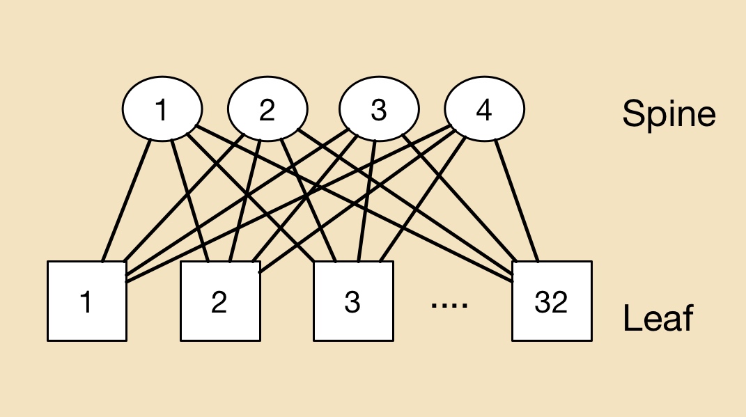
In the data centre, a common switching arrangement used to interconnect servers is the leaf-and-spine architecture. A ‘leaf’ is typically a top-of-rack switch while the ‘spine’ is a larger capacity switch.
A top-of-rack switch typically uses 10 gigabit links to connect to the servers. The connection between the leaf and spine is typically a higher capacity link - 40 or 100 gigabit. A common arrangement is to adopt a 3:1 oversubscription - the total input capacity to the leaf switch is 3x that of its output stream.
To illustrate the point with numbers, a 640 gigabit top-of-rack switch is assumed, 480 gigabit (or 48 x10 Gig) capacity used to connect the servers and 160 gigabit (4 x 40 Gig) to link the top-of-rack switch to the spine switches.
In the example shown (Figure 4) there are 32 leaf and four spine switches connecting a total of 1,536 servers.
 Figure 4: An example to show the principles of a leaf and spine architecture in the data centre. Source: Gazettabyte
In a data centre with 100,000 servers, clearly a more complicated interconnection scheme involving multiple leaf and spine clusters is required.
Arista Network’s White Paper details data centre switching and leaf-and-spine arrangements, while Facebook published a blog (and video) discussing just how complex an interconnection network can be (see Figure 5).
 Figure 5: How multiple leaf and spines can be connected in a large scale data centre. Source: Facebook
Rockley demos a silicon photonics switch prototype
Rockley Photonics has made a prototype switch to help grow the number of servers that can be linked in a data centre. The issue with interconnection networks inside a data centre is that they do not scale linearly as more servers are added.
 Dr. Andrew Rickman
“If you double the number of servers connected in a mega data centre, you don’t just double the complexity of the network, it goes up exponentially,” explains Andrew Rickman, co-founder, chairman and CEO at Rockley Photonics. “That is the problem we are addressing.”
By 2017 and 2018, it will still be possible to build the networks that large-scale data centre network operators require, says Rickman, but at an ever increasing cost and with a growing power consumption. “The basic principles of what they are doing needs to be rethought,” he says.
Network scale
Modern data centre networks must handle significant traffic flow between servers, referred to as east-west traffic. A common switching arrangement in the data centre is the leaf-spine architecture, used to interconnect thousands of servers.
A ‘leaf’ may be a top-of-rack switch that is linked to multiple server chassis on one side and larger-capacity, ‘spine’ switches on the other. The result is a switch network where each leaf is connected to all the spine switches, while each spine switch is linked to all the leaves. In the example shown, four spine switches connect to 32 leaf switches.
 A leaf-spine architecture
The leaf and spine switches are built using ASICs, with the largest ICs typically having 32, 100 gigabit ports. One switch ASIC may be used in a platform but as Rickman points out, larger switches may implement multiple stages such as a three-stage Clos architecture. As a result, traffic between servers on different leaves, travelling up and down the leaf-spine, may pass through five stages or hops but possibly as many as nine.
There is no replacement performance in this area
It is the switch IC’s capacity and port count that dictates the overall size of the leaf-spine network and therefore the number of servers that can be connected. Rockley’s goal is to develop a bigger switch building block making use of silicon photonics.
“The fundamental thing to address is making bigger switching elements,” says Rickman. “That way you can keep the number of stages in the network the same but still make bigger and bigger networks.” Rockley expects its larger building-block switch will reduce the switch stages needed.
The UK start-up is not yet detailing its switch beyond saying it uses optical switching and that the company is developing a photonic integrated circuit (PIC) and a controlling ASIC.
“In the field of silicon photonics, for the same area of silicon, you can produce a larger switch; you have more capacity than you do in electronics,” says Rickman. Moreover, Rockley says that its silicon photonics-based PIC will scale with Moore’s law, with its switch's data capacity approximately doubling every two years. “Previously, the network did not scale with Moore’s law,” says Rickman.
Customers can see something is real and that it works. We are optimising all the elements of the system before taping out the fully integrated devices
Status
The company has developed a switch prototype that includes ‘silicon photonics elements’ and FPGAs. “Customers can see something is real and that it works,” says Rickman. “We are optimising all the elements of the system before taping out the fully integrated devices.” Rockley expects to have its switch in volume production in 2017.
Last year the company raised its first round of funding and said that it would undergo a further round in 2015. Rockley has not said how much it has raised or the status of the latest round. “We are well-funded and we have a very supportive group of investors,” says Rickman.
Rickman has long been involved in silicon photonics, starting out as a researcher at the University of Surrey developing silicon photonics waveguides in the early 1990s, before founding Bookham Technologies (now Oclaro). He has also been chairman of silicon photonics start-up Kotura that was acquired by Mellanox Technologies in 2013. Rickman co-founded Rockley in 2013.
“What I’ve learned about silicon photonics, and about all those electronics technologies, is how to design stuff from a process point of view to make something highly manufacturable and at the same time having the performance,” says Rickman.
There is no replacement performance in the area of data centre switching, he stresses: “The benefit of our technology is to deliver the performance, not the fact that it is cheap or [offers] average performance.”
For Part 2, Interconnection networks - an introduction, click here
Choosing paths to future Gigabit Ethernet speeds
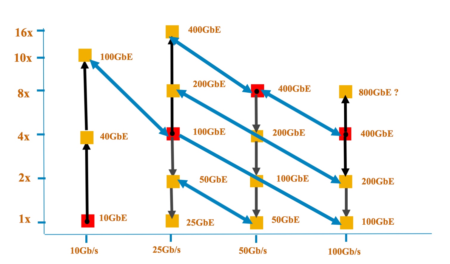 The y-axis shows the number of lanes while the x-axis is the speed per lane. Each red dot shows the Ethernet rate at which the signalling (optical or electrical) was introduced. One challenge that John D'Ambrosia highlights is handling overlapping speeds. "What do we do about 100 Gig based on 4x25, 2x50 and 1x100 and ensure interoperability, and do that for every multiple where you have a crossover?" Source: Dell
One catalyst for these discussions has been the progress made in the emerging 400 Gigabit Ethernet (GbE) standard which is now at the first specification draft stage.
“If you look at what is happening at 400 Gig, the decisions that were made there do have potential repercussions for new speeds as well as new signalling rates and technologies,” says John D’Ambrosia, chairman of the Ethernet Alliance.
Before the IEEE P802.3bs 400 Gigabit Ethernet Task Force met in July, two electrical signalling schemes had already been chosen for the emerging standard: 16 channels of 25 gigabit non-return-to-zero (NRZ) and eight lanes of 50 gigabit using PAM-4 signalling.
For the different reaches, three of the four optical interfaces had also been chosen, with the July meeting resolving the fourth - 2km - interface. The final optical interfaces for the four different reaches are shown in the Table.

The adoption of 50 gigabit electrical and optical interfaces at the July meeting has led some industry players to call for a new 50 gigabit Ethernet family to be created, says D’Ambrosia.
Certain players favour the 50 GbE standard to include a four-lane 200 GbE version, just as 100 GbE uses 4 x 25 Gig channels, while others want 50 GbE to be broader, with one, two, four and eight lane variants to deliver 50, 100, 200 and 400 GbE rates.
If you look at what is happening at 400 Gig, the decisions that were made there do have potential repercussions for new speeds as well as new signalling rates and technologies
The 400 GbE standard’s adoption of 100 GbE channels that use PAM-4 signalling has also raised questions as to whether 100 GbE PAM-4 should be added to the existing 100 GbE standard or a new 100 GbE activity be initiated.
“Those decisions have snowballed into a lot of activity and a lot of discussion,” says D’Ambrosia, who is organising an activity to address these issues and to determine where the industry consensus is as to how to proceed.
“These are all industry debates that are going to happen over the next few months,” he says, with the goal being to better meet industry needs by evolving Ethernet more quickly.
Ethernet continues to change, notes D’Ambrosia. The 40 GbE standard exploited the investment made in 10 gigabit signalling, and the same is happening with 25 gigabit signalling and 100 gigabit.
If you buy into the idea of more lanes based around a single signalling speed, then applying that to the next signalling speed at 100 Gigabit Ethernet, does that mean the next speed with be 800 Gigabit Ethernet?
With 50 Gig electrical signalling now starting as part of the 400 GbE work, some industry voices wonder whether, instead of developing one Ethernet family around a rate, it is not better to develop a family of rates around the signalling speed, such as is being proposed with 50 Gig and the use of 1, 2, 4 and 8 lane configurations.
“If you buy into the idea of more lanes based around a single signalling speed, then applying that to the next signalling speed at 100 Gigabit Ethernet, does that mean the next speed with be 800 Gigabit Ethernet?” says D’Ambrosia.
The 400 GbE Task Force is having its latest meeting this week. A key goal is to get the first draft of the standard - Version 1.0 - approved. “To make sure all the baselines have been interpreted correctly,” says D’Ambrosia. What then follows is filling in the detail, turning the draft into a technically-complete document.
Further reading:
LightCounting: 25GbE almost done but more new Ethernet options are coming, click here
Verizon prepares its next-gen PON request for proposal
 Vincent O'Byrne
The NG-PON2 request for proposal (RFP) is being issued after the US operator completed a field test that showed a 40 gigabit NG-PON2 system working alongside Verizon’s existing GPON customer traffic.
The field test involved installing a NG-PON2 optical line terminal (OLT) at a Verizon central office and linking it to a FiOS customer’s home 5 km away. A nearby business location was also included in the trial.
Cisco and PT Inovação, an IT and research company owned by Portugal Telecom, worked with Verizon on the trial and provided the NG-PON2 equipment.
NG-PON2 is the follow-on development to XG-PON1, the 10 gigabit GPON standard. NG-PON2 supports both point-to-point links and a combination of time- and wavelength-division multiplexing that in effect supports a traditional time-division multiplexed PON per wavelength, known as TWDM-PON. The rates TWDM-PON supports include 10 gigabit symmetrical, 10 gigabit downstream and 2.5 gigabit upstream, and 2.5 gigabit symmetrical.
Verizon field-tested the transmission of NG-PON2 signals over a fibre already carrying GPON traffic to show that the two technologies can co-exist without interference, including Verizon’s analogue RF video signal. Another test demonstrated how, in the event of a OLT card fault at the central office, the customer’s optical network terminal (ONT) equipment can detect the fault and retune to a new wavelength, restoring the service within seconds.
Now we know we can deploy this technology on the same fibre without interference and upgrade the customer when the market demands such speed
Verizon is not saying when it will deploy the next-generation access technology. “We have not said as the technology has to become mature and the costs to reduce sufficiently,” says Vincent O'Byrne, director of access technology for Verizon.
It will also be several years before such speeds are needed, he says. “But now we know we can deploy this technology on the same fibre without interference and upgrade the customer when the market demands such speed.”
Verizon expects first NG-PON2 services will be for businesses, while residential customers will be offered the service once the technology is mature and cost-effective, says O’Byrne.
Vodafone is another operator conducting a TWDM-PON field trial based on four 10 gigabit wavelengths, using equipment from Alcatel-Lucent. Overall, Alcatel-Lucent says it has been involved in 16 customer TWDM-PON trials, half in Asia Pacific and the rest split between North America and EMEA.
Further reading
For an update on the NG-PON2 standard, click here
US invests $610 million to spur integrated photonics
 Prof. Duncan Moore
Dubbed the American Institute for Manufacturing Integrated Photonics (AIM Photonics), the venture has attracted 124 partners includes 20 universities and over 50 companies.
The manufacturing innovation institute will be based in Rochester, New York, and will be led by the Research Foundation for the State University of New York. A key goal is that the manufacturing institute will continue after the initiative is completed in early 2021.
We are at the point in photonics where we were in electronics when we still had transistors, resistors and capacitors. What we are trying to do now is the equivalent of the electronics IC
While the focus is on photonic integrated circuits, the expectation is that the venture will end up being broader. “NASA, the Department of Energy and the Department of Defense are all interested in using this as a vehicle for doing other work,” says Duncan Moore, professor of optics at the University of Rochester.
The venture will address such issues as design, on-chip manufacturing, packaging and assembly of PICs. “We are at the point in photonics where we were in electronics when we still had transistors, resistors and capacitors,” says Moore. “What we are trying to do now is the equivalent of the electronics IC.”
"It is an amazing public-private consortium utilizing an unprecedented $610 million investment in photonics," says Richard Soref, a silicon photonics pioneer and a Group IV photonics researcher. "The large and powerful team of world-class investigators is likely to make research-and-development progress of great importance for the US and the world.”
Project plans
The first six months are being used to fill in project’s details. “There are overall budget numbers but individual projects are not well defined in the proposal,” says Moore, adding that many of the subfields - packaging, sensors and the like - will be defined and request-for-proposals issued.
An executive committee will then determine which projects are funded and to what degree. Project durations will vary from one-offs to the full five years.
The large and powerful team of world-class investigators is likely to make research-and-development progress of great importance for the US and the world
Companies backing the project include indium phosphide specialist Infinera as well as silicon photonics players Acacia Communications, Aurrion, and Intel. How the two technologies as well as Group IV photonics will be accommodated as part of the manufacturing base is still to be determined, says Prof. Moore. His expectation is that all will be investigated before a ‘shakeout’ will occur as the venture progresses.
The focus will be on telecom wavelengths and the mid-wave 3 to 5 micron band. “There are a lot of applications in that [longer] wavelength band: remote sensing, environmental analysis, and for doing things on the battlefield,” says Moore.
A public document will be issued around the year-end describing the project’s organisation.
Further information:
The White House factsheet, click here
A Photonics video interview with the chairman of the institute, Professor Robert Clark, click here
Micro QSFP module to boost equipment port densities
 Nathan Tracy
The μQSFP will support both copper and optical cabling, and will have an improved thermal performance, benefitting interfaces and platforms.
“There is always a quest for greater port density or aggregate bandwidth,” says Nathan Tracy, technologist at TE Connectivity and chair of the μQSFP MSA.
The challenge for the module makers is to provide denser form factors to increase overall system traffic. “As we go to higher densities, we are also increasing the thermal load,” says Tracy. “And so now it is a mechanical and a thermal [design] problem, and both need to be solved jointly.”
The thermal load is increased since the μQSFP supports interfaces that consume up to 3.5 W - like the QSFP - while having the width of the smaller SFP rated at 1.5 W.
“We are limited in the directions we can pull the heat out,” says Tracy. “If we are going to enable a higher density form factor that has the same width as an SFP but it is going to have the functionality of a QSFP, now we have a problem.”
This requires the MSA engineers to develop new ways to rid the μQSFP of its heat.
If we are going to enable a higher density form factor that has the same width as an SFP but it is going to have the functionality of a QSFP, now we have a problem
Heat transfer and other challenges
The volume and surface area of a module determine the overall thermal capacity or thermal density. The module can be modelled as an electrical circuit, with heat flow equivalent to current, while each interface has a thermal resistance.
There are three interfaces - thermal resistances - associated with a module: between the heat source and the module case, the case and the heat sink, and the heat sink and ambient air. These three thermal resistances are in series and the goal is to reduce them to ensure greater heat flow.
The module’s circuitry generates heat and the interface between the circuitry and the module’s case is one of the thermal resistances. “You are going to have a heat source in the module and no matter what you do, there is going to be some thermal resistance from that source to the module housing,” says Tracy.
You have to get good signal integrity through that electrical interface because we are working at 25 gigabit-per-second (Gbps) data rates today and we know 50 Gbps data rates are coming
The second thermal resistance - one that the µQSFP eliminates - is between the module housing and the heat sink. Sliding a module into its cage puts it into contact with the heat sink. But the contact between the two surfaces is imperfect, making heat extraction harder. Building the heat sink into the μQSFP module avoids using the sliding design.
The remaining thermal resistance is between the heat sink and the cooling air blown through the equipment. This thermal resistance between the heat sink's metal fin structure and the air flow exists however good the heat sink design, says Tracy.
Other design challenges include achieving signal integrity when cramming the four electrical lanes across the µQSFP’s smaller width, especially when its support 25 Gbit/s lanes and likely 50 Gbit/s in future, says Tracy.
And the module's optical interface must also support duplex LC and MPO connectors to interoperate with existing cabling.
“It is all a balancing act,” says Tracy.
Applications
The μQSFP is aimed at platforms such as 4.8 and 6.4 Tbps capacity switches. The QSFP is used for current 3.2 Tbps platforms but greater port densities will be needed for these next-generation platforms. The size of the μQSFP means 48 ports will fit in the space 36 QSFPs currently occupy, while 72 μQSFPs will fit on a line card if three rows are used.
The μQSFP may also find use outside the data centre for longer, 100 km reaches. “Today you can buy SFP modules that go 100 km,” says Tracy. “With this form factor, we are creating the capability to go up to four lanes in the same width as an SFP and, at the same time, we are improving the thermal performance significantly over what an SFP can do.”
The Micro QSFP group is not saying when the µQSFP MSA will be done. But Tracy believes the μQSFP would be in demand were it available now. Its attraction is not just the greater port density, but how the µQSFP would aid systems engineers in tackling their thermal design challenges.
The pluggable form factor will allow air to flow from the face plate and through the module to where ICs and other circuitry reside. Moreover, since 32 μQSFP ports will take up less face-plate area than 32 QSFPs, perforations could be added, further improving airflow.
“If you look at the QSFP or SFP, it does not allow airflow through the cage from the front [plate] to the back,” says Tracy.
The μQSFP MSA founding members are Avago Technologies, Broadcom, Brocade, Cisco, Dell, Huawei, Intel, Lumentum (formerly JDSU), Juniper Networks, Microsoft, Molex, and TE Connectivity.