
Reflections on OFC 2017
Mood, technologies, notable announcements - just what are the metrics to judge the OFC 2017 show held in Los Angeles last week?
It was the first show I had attended in several years and the most obvious changes were how natural the presence of the internet content providers now is alongside the telecom operators, as well as systems vendors exhibiting at the show. Chip companies, while also present, were fewer than before.
 Source: OSA
Another impression were the latest buzz terms: 5G, the Internet of Things and virtual reality-augmented reality. Certain of these technologies are more concrete than others, but their repeated mention suggests a consensus that the topics are real enough to impact optical components and networking.
It could be argued that OFC 2017 was the year when 400 Gigabit Ethernet became a reality
The importance of 5G needs no explanation while the more diffuse IoT is expected to drive networking with the huge amounts of data it will generate. But what are people seeing about virtual reality-augmented reality that merits inclusion alongside 5G and IoT?
Another change is the spread of data rates. No longer does one rate represent the theme of an OFC such as 40 Gigabits or 100 Gigabits. It could be argued that OFC 2017 was the year when 400 Gigabit Ethernet became a reality but there is now a mix of relevant rates such as 25, 50, 200 and 600 gigabits.
Highlights
There were several highlights at the show. One was listening to Jiajin Gao, deputy general manager at China Mobile Technology, open the OIDA Executive Forum event by discussing the changes taking place in the operator's network. Gao started by outlining the history of China Mobile's network before detailing the huge growth in ports at different points in the network over the last two years. He then outlined China Mobile's ambitious rollout of new technologies this year and next.
China's main three operators have 4G and FTTx subscriber numbers that dwarf the rest of the world. Will 2017 eventually be seen as the year when the Chinese operators first became leaders in telecom networking and technologies?
The Executive Forum concluded with an interesting fireside discussion about whether the current optical market growth is sustainable. The consensus among representatives from Huawei, Hisense, Oclaro and Macom was that it is; that the market is more varied and stable this time compared to the boom and bust of 1999-2001. As Macom’s Preetinder Virk put it: "The future has nothing to do with the past". Meanwhile, Huawei’s Jeffrey Gao still expects strong demand in China for 100 gigabits in 2017 even if growth is less strong than in 2016. He also expects the second quarter this year to pick up compared to a relatively weak first quarter.
OFC 2017 also made the news with an announcement that signals industry change: Ciena's decision to share its WaveLogic Ai coherent DSP technology with optical module vendors Lumentum, Oclaro and NeoPhotonics.
The announcement can be viewed several ways. One is that the initiative is a response to the success of Acacia as a supplier of coherent modules and coherent DSP technology. System vendors designed their own coherent DSP-ASICs to differentiate their optical networking gear. This still holds true but the deal reflects how the progress of merchant line-side optics from the likes of Acacia is progressing and squeezing the scope for differentiation.
The deal is also a smart strategic move by Ciena which, through its optical module partners, will address new markets and generate revenues as its partners start to sell modules using the WaveLogic Ai. The deal also has a first-mover advantage. Other systems vendors may now decide to offer their coherent DSPs to the marketplace but Ciena has partnerships with three leading optical module makers and is working with them on future DSP developments for pluggable modules.
The deal also raises wider questions as to the role of differentiated hardware and whether it is subtly changing in the era of network function virtualisation, or whether it is a reflection of the way companies are now collaborating with each other in open hardware developments like the Telecom Infra Project and the Open ROADM MSA.
Another prominent issue at the show is the debate as to whether there is room for 200 Gigabit Ethernet modules or whether the industry is best served by going straight from 100 to 400 Gigabit Ethernet.
Facebook and Microsoft say they will go straight to 400 gigabits. Cisco agrees, arguing that developing an interim 200 Gigabit Ethernet interface does not justify the investment. In contrast, Finisar argues that 200 Gigabit Ethernet has a compelling cost-per-bit performance and that it will supply customers that want it. Google supported 200 gigabits at last year’s OFC.
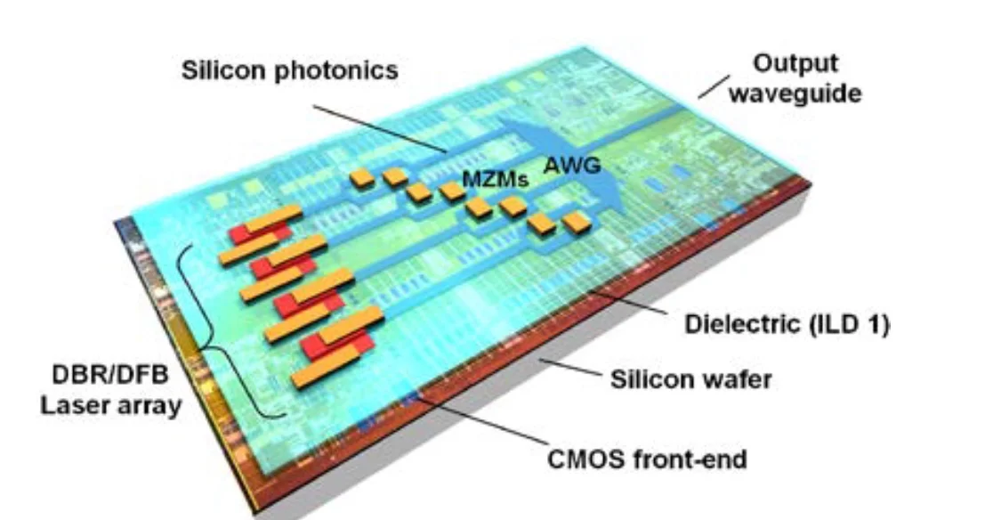
Silicon photonics
Silicon photonics was one topic of interest at the show and in particular how the technology continues to evolve. Based on the evidence at OFC, silicon photonics continues to progress but there were no significant developments since our book (co-written with Daryl Inniss) on silicon photonics was published late last year.
One of the pleasures of OFC is being briefed by key companies in rapid succession. Intel demonstrated at its booth its silicon photonics products including its CWDM4 module which will be generally available by mid-year. Intel also demonstrated a 10km 4WDM module. The 4WDM MSA, created last year, is developing a 10km reach variant based on the CWDM4, as well as 20km and 40km based designs.
Meanwhile, Ranovus announced its 200-gigabit CFP2 module based on its quantum dot laser and silicon photonics ring resonator technologies with a reach approaching 100km. The 200 gigabit is achieved using 28Gbaud optics and PAM-4.
Elenion Technologies made several announcements including the availability of its monolithically integrated coherent modulator receiver after detailing it was already supplying a 200 gigabit CFP2-ACO to Coriant. The company was also demonstrating on-board optics and, working with Cavium, announced a reference architecture to link network interface cards and switching ICs in the data centre.
I visited Elenion Technologies in a hotel suite adjacent to the conference centre. One of the rooms had enough test equipment and boards to resemble a lab; a lab with a breathtaking view of the hills around Los Angeles. As I arrived, one company was leaving and as I left another well-known company was arriving. Elenion was using the suite to demonstrate its technologies with meetings continuing long after the exhibition hall had closed.
Two other silicon photonics start-ups at the show were Ayar Labs and Rockley Photonics.
Ayar Labs in developing a silicon photonics chip based on a "zero touch" CMOS process that will sit right next to complex ASICs and interface to network interface cards. The first chip will support 3.2 terabits of capacity. The advantage of the CMOS-based silicon photonics design is the ability to operate at high temperatures.
Ayar Labs is using the technology to address the high-bandwidth, low-latency needs of the high-performance computing market, with the company expecting the technology to eventually be adopted in large-scale data centres.
Rockley Photonics shared more details as to what it is doing as well as its business model but it is still to unveil its first products.
The company has developed silicon photonics technology that will co-package optics alongside ASIC chips. The result will be packaged devices with fibre-based input-output offering terabit data rates.
Rockley also talked about licensing the technology for a range of applications involving complex ICs including coherent designs, not just for switching architectures in the data centre that it has discussed up till now. Rockley says its first product will be sampling in the coming months.
Looking ahead
On the plane back from OFC I was reading The Undoing Project by Michael Lewis about the psychologists Danny Kahneman and Amos Tversky and their insights into human thinking.
The book describes the tendency of people to take observed facts, neglecting the many facts that are missed or could not be seen, and make them fit a confident-sounding story. Or, as the late Amos Tversky put it: "All too often, we find ourselves unable to predict what will happen; yet after the fact, we explain what did happen with a great deal of confidence. This 'ability' to explain that which we cannot predict, even in the absence of any additional information, represents an important, though subtle, flaw in our reasoning."
So, what to expect at OFC 2018? More of the same and perhaps a bombshell or two. Or to put it another way, greater unpredictability based on the impression at OFC 2017 of an industry experiencing an increasing pace of change.
Presentation slides of the book
 A set of slides summarising the book, Silicon Photonics: Fueling the Next Information Revolution.
To download the slides, please click here.
Silicon Photonics Merging Ahead
"Silicon photonics has made considerable progress in a relatively short time to emerge as an important systems technology whose time has come"
FSAN unveils roadmap plans
Part 2: Next-generation passive optical networks
The Full Service Access Network (FSAN) has outlined its vision for fibre access networks for the coming decade.
FSAN is an industry forum that includes over 20 operators and 70 members overall. The group identifies service requirements and develops optical access technologies that are passed to the International Telecommunication Union (ITU) for standardisation.
 Source: FSAN
“One of the messages of the roadmap is that, in the immediate future, what FSAN wants to do is evolve the existing standards,” says Peter Dawes, FSAN NGPON co-chair.
The latest FSAN technologies to become standards are XGS-PON (10 gigabits symmetrical passive optical network) and the multiple wavelength TWDM-PON (time wavelength-division multiplexing passive optical network), also known as NG-PON2 (see chart).
PON status
XGS-PON is a single-wavelength PON standard that supports two rates: a 10-gigabit symmetrical rate and the asymmetrical 10 gigabits downstream (to the user) and 2.5 gigabits upstream originally introduced by XG-PON.
 Peter Dawes
TWDM-PON uses four wavelengths to deliver up to 40 gigabits of symmetrical bandwidth and has an option for eight wavelengths overall. TWDM-PON also uses tuneable lasers enabling operators to move subscribers between wavelengths.
“FSAN operators see continued growth in PON deployment,” says Dawes. “There is still strong deployment of GPON and we are on the verge of needing 10-gigabit symmetrical services.” Other operators may delay and go straight to TWDM-PON, he says.
According to Dawes, operators are seeing a variety of applications that are driving the need for 10-gigabit access rates. One is the growing use of video and video conferencing. Another bandwidth driver for access networks is mobile applications such as connecting mobile antennas and mobile backhaul. In addition, there are digital home trends such as social networking and the moving of content to the cloud.
Mobile fronthaul can eat as much bandwidth as you can supply once you start to aggregate [radio] antennas
Operators are also keen to attach the labels ‘gigabit’ and ‘gigabit services’ to their broadband offerings as a marketing differentiator.
Other drivers for the move to the newer PON technologies include peer-to-peer services and business IP services, says Dawes.
Roadmap
FSAN’s plan to evolve the existing standards in the near term will take the group to 2021.
One obvious way the existing PONs can be evolved is to adopt 25-gigabit wavelengths. This would enable a 25-gigabit symmetrical extension to XGS-PON and a future TWDM-PON variant with up to 200 gigabits of capacity if the full eight wavelengths are used. “It is a case of looking for logical evolutions of these technologies,” says Dawes.
One application that could use such high capacities is mobile fronthaul, says Dawes: “It can eat as much bandwidth as you can supply once you start to aggregate [radio] antennas.”
After 2020, FSAN will investigate disruptive technologies as it defines future optical access schemes. R&D work, new modulation schemes and component developments including silicon photonics will all be assessed as to their suitability for future optical access schemes.
Meanwhile, FSAN says it will review its roadmap on a yearly basis and amend it as required.
See Part 1: XGS and TWDM passive optical networks, click here
Elenion unveiled as a silicon photonics PIC company
- Elenion Technologies is making silicon photonics-based photonic integrated circuits
- The company has been active for two and a half years and has products already deployed
A privately-owned silicon photonics company that is already shipping products has dropped its state of secrecy to announce itself. Elenion Technologies is owned by Marlin Equity Partners, the investment firm that also owns systems vendor, Coriant.
“We are in the [optical] engine business,” says Larry Schwerin, CEO of Elenion Technologies. “We are developing a platform leveraging silicon photonics but we have other capabilities.”
 Larry SchwerinElenion’s expertise includes indium phosphide, radio frequency integrated circuits (RFICs), packaging, and driver and control electronics circuit design. The RFIC expertise suggests the company also plans to address the mobility market.
The company will detail its first products prior to the OFC show next March.
Telecom and Datacom
Elenion’s initial focus is the telecom market where its products are already deployed, with Coriant being a likely early customer. “We are also very active in datacom which has a different set of requirements,” says Schwerin.
Telecom is the harder 'trade space' of the two segments, says Schwerin. Telecom designs have to be outside-plant hardened and Telcordia-compliant. “Proving that world is a good place to get started and focussed,” he says.
In contrast, the datacom market has shorter equipment life cycles with optical designs deployed in a more controlled environment. Datacom customers also don't just want pluggables. “They want on-board solutions, parallel solutions, and they request a cost of $1-per-gigabit,” says Schwerin.
The company is targeting optical module makers, systems vendors and the cloud operators
The challenges facing the large-scale data centre operators are multifold: how they drive more bandwidth to the server, how they make the server more effective, how they scale their switching fabric, how they better use their fibre infrastructure and how they meet their optics cost targets.
Elenion says it has detailed data on the construction and costs of data centres and how they will scale. "You need to have that expertise in order to design the platform that they are trying to do today and going forward," says Schwerin. The company is working to deliver an optical engine that will help the data centre operators address the issues of distance, power consumption, space and signal integrity, and which will meet their $1-per-gigabit cost target.
We have developed a set of tools and a set of expertise that lets us design very complex integrated optoelectronic systems at the chip scale
Expertise
Elenion is limited in what it can say until its first products are unveiled. What is clear is that the silicon photonics company has a photonic integrated circuit (PIC) capability that it is using for on-board optics and for pluggable designs such as the CFP2.
 Michael Hochberg
“We have developed a set of tools and a set of expertise that lets us design very complex integrated opto-electronic systems at the chip scale,” says Michael Hochberg, CTO of Elenion.
According to Hochberg, Elenion is pulling complexity out of other systems and putting it into silicon. The value of such PICs is that it avoids having to deploy discrete optics such as lenses. And silicon is the ideal platform for scaling complexity, says Hochberg: “All the areas that we have developed expertise are things that we believe will need to be co-designed with the PIC.”
In the electronics industry, you tape things out and you expect them to work. That is what we are replicating here.
The company says it is building up a capability that has long existed in the semiconductor industry. "In the electronics industry, you tape things out and you expect them to work," says Hochberg. "That is what we are replicating here."
For datacom applications, Schwerin says that in addition to the PIC’s function, the company has developed a wafer-scale approach to packaging. Here, devices are packaged while still on the wafer rather than having to dice the wafer first. “You have got to get into the volumes of millions, not tens or hundreds of thousands,” says Schwerin. “That forces you into that space.”
The company is targeting optical module makers, systems vendors and the cloud operators as customers.
Origins
Schwerin was formerly the CEO of Capella Intelligent Subsystems, a developer of wavelength-selective switch technology, that was sold to Alcatel-Lucent (now Nokia) in 2013.
Hochberg was a director at the Optoelectronic Systems in Silicon (OpSIS) foundry and was a co-founder of silicon photonics company, Luxtera.
The two first met at a conference when Hochberg was running Silicon Lightwave Services (SLS), a silicon photonics design-for-service company. Schwerin became CEO of SLS and the company was bought by Merlin two and a half years ago to become Elenion. The name Elenion means starlight, a nod to J.R.R. Tolkien’s novels.
“We are now introducing ourselves as we are getting enough requests that it seemed the appropriate time,” says Schwerin.
DIMENSION tackles silicon photonics’ laser shortfall
Several companies and research institutes, part of a European project, are developing a silicon photonics process that combines on-chip electronics and lasers. Dubbed Dimension (Directly Modulated Lasers on Silicon), the silicon photonics project is part of the European Commission’s Horizon 2020 research and innovation programme.
 The Dimension process showing the passive photonics, dielectric material, BiCMOS circuitry, and the on-chip lasers and modulators. The indium phosphide material is shown in red. Source: Dimension.
Goal
Silicon photonics has long been seen as a technology having the potential to deliver optical devices at CMOS manufacturing costs. But silicon's key shortfall is that it does not lase. “What we see with today’s solutions is a very low-cost chip with a lot of functionality, which is a great thing, but in addition you need lasers,” says Bert Offrein, principal research staff member and manager of neuromorphic devices and systems at IBM Research, a participant in the Dimension project.
The laser accounts for a relatively large fraction of the total bill of materials of a silicon photonics chip. In turn, connecting the light source to the chip is not trivial and adds to the packaging costs. “In this project, we try to tackle this [laser] issue,” says Offrein.
The project's goal is to develop manufacturing processes that will enable the integration of photonics, including the laser, and electronics, all on one chip. “By fully integrating the laser on the chip, we massively reduce the cost and create additional functionality,” says Offrein.
“This is the true embodiment of what people first pictured as silicon photonics: the combination of optics and electronics on a single chip,” says Lars Zimmermann, team leader, silicon photonics at the Innovations for High Performance Microelectronics (IHP) research institute, another member of Dimension.
Proof-of-concept demonstrators
Dimension is a four-year project that will end in early 2020. Other project participants besides IBM Research and the IHP include ADVA Optical Networking, Opticap and the Athens Information Technology (AIT) research centre. The Dresden University of Technology is overseeing the project.
The project has set itself the goal of producing three proof-of-concept designs using the integrated silicon photonics technology.
One is a 400 Gigabit Ethernet (GbE) transmitter made up of eight 50 gigabit-per-second (Gbps) channels, each comprising a 25 gigabaud directly-modulated laser combined with 4-level pulse amplitude modulation (PAM4). Two variants are planned: a directly modulated version for the 400GbE 2km reach specification, and one with external modulation for the 400GbE 10km reach standard.
Another design is a coherent transmitter for such applications as data centre interconnect, compromising a monolithically integrated narrow-linewidth tunable laser, modulator and driver. The coherent transmitter will have a 10km target reach, will operate at 25Gbps and have a tunable narrow linewidth of under 1MHz.
The third, final demonstrator is a directly-modulated 25-gigabit non-return-to-zero laser using indium phosphide grown directly on the silicon.
By fully integrating the laser on the chip, we massively reduce the cost and create additional functionality
Process details
The silicon photonics manufacturing process involves using a silicon-on-insulator (SOI) wafer to implement the passive photonics functions and the electronics. The electronics supports high-speed analogue driver transistors and a 0.25-micron BiCMOS process used to implement the chip's control logic and control interfaces.
 Bert Offrein
The laser is constructed by first bonding a thin layer of indium phosphide. “It is structured in such a way that it [the III-V material] can be embedded completely in the whole CMOS processing,” says Offrein.
The indium phosphide layer, referred to as a III-V membrane, sits on a thin dielectric layer placed on the SOI wafer. The dielectric material is needed to protect the wafer from contamination by the III-V material and ensure that such a design could be manufactured in a BiCMOS foundry.
Once the thin indium phosphide layer is deposited, the laser can be constructed. The final stages, part of the chip-making back-end process, is the adding of metallisation layers that connect the laser and the electronics, and the circuits to the interface signals.
Growing lasers on silicon
Growing the indium phosphide layer directly on silicon, as will be done for the third demonstrator, is more exploratory. “We want to show there is a path forward on this III-V-on-silicon technology to reduce the cost further,” says Offrein.
 Lars Zimmermann
The challenge growing indium phosphide on silicon is the lattice mismatch that occurs between the two materials which leads to defects.
To tackle the issue, an approach known as confined growth is used. A small ‘seed’ is put on the silicon to act as a growth point for the indium phosphide. A small cavity is created using silica to confine the resulting growth. “The material grows in this glass cavity and the defects grow out and disappear at the edges,” says Offrein. “You then have a very high-quality III-V in this glass and this is the starting point to continue to build the quantum wells that we need.”
One challenge is enlarging the confined growth area. So far, such growth is limited to a micron whereas the length of a laser can be 500 microns typically. And once the laser is built, there remain the issues of laser reliability and temperature stability. “We will see challenges but we are not there yet,” says Offrein.
This is the true embodiment of what people first pictured as silicon photonics: the combination of optics and electronics on a single chip
Status
Dimension is tackling designs for communications but such on-chip lasers will also be useful for a range of applications such as optical sensing, says Offrein.
The project is coming to the end of its first year. Its members are creating the basic building blocks needed to realise the lasers on the silicon wafer. IBM has demonstrated the basic functionality by bonding indium phosphide to its own passive silicon photonics technology. “We have also realised the first lasers - not yet electrically pumped but optically pumped,” says Offrein. The performance of these lasers is now being characterised.
All the processes needed to pump the lasers electrically are now in place and the goal is to build complete laser structures by March 2017.
IBM is also working with IHP to see what is required to implement the technology using IHP’s own silicon photonics process. IHP is currently testing IBM’s wafers regarding any contamination issues before testing the integration process.
ADVA Optical Networking would not be on board if they were not expecting eventually to have such technology available for their products
Exploitation
The European Commission has a long history of programmes backing leading-edge research. However, Europe's track record of exploiting such research to achieve market-leading companies and products has been limited.
The European Commission staff involved in planning the Horizon 2020 projects have been far more active in ensuring that these projects are exploited, says Zimmermann. "ADVA Optical Networking would not be on board if they were not expecting eventually to have such technology available for their products," he adds.
If Dimension proves successful, IHP could make available the integrated silicon photonics process to companies to implement their opto-electronic integrated circuit designs.
IBM, while no longer a semiconductor manufacturer, would also be keen for the technology to be transferred to large foundries such as STMicroelectronics and GlobalFoundries. “That way we could purchase the technology and apply it in our own systems,” says Offrein.
Article amended on Nov 29th. Added details about the proof-of-concept demonstrators.
The making of integrated optics
A US initiative is bringing together leading companies with top academics and universities to create a manufacturing infrastructure for the widespread adoption of integrated photonics.
The US sees integrated photonics as a strategic technology and has set up the American Institute for Manufacturing Integrated Photonics - AIM Photonics - to advance the technology and make it available to a wider community of companies. AIM Photonics, with $610 million of public and private funding, is a five-year initiative ending in 2020. AIM’s long-term goal is to be self-sustaining.
 Doug Coolbaugh
“Right now the infrastructure is focussed on electronics and CMOS but photonics is going to be the future,” says Doug Coolbaugh, chief operations officer at AIM Photonics. “There is no other way to do it [very high bandwidth] except using light for ultra fast communications.”
Technologies start at universities and in the labs of companies with large R&D budgets. IBM and Intel, for example, have been developing silicon photonics for over a decade and the technology is ready for deployment. However, the intellectual property developed remains with such companies.
“AIM is not only creating the manufacturing infrastructure for integrated photonics but also ideas and intellectual property that can be used by companies for new products,” says Coolbaugh.
All the elements are being addressed so that small to medium businesses and entrepreneurial ventures can use integrated photonics for their products; companies too small to develop the technology themselves. “That will accelerate the silicon photonics ecosystem and allow new products to come out much faster than it would normally take,” says Coolbaugh.
Manufacturing
Silicon photonics luminary, Lionel Kimerling, professor of materials science and engineering at MIT, and an active member of AIM Photonics, views its focus on manufacturing as an important development.
The discipline of manufacturing is something that the chip industry has mastered through designing process integration, selecting materials and all the qualification standards used to meet system requirements, he says, but is less developed in the photonics industry.
AIM is making available a chip fabrication plant to interested companies. SUNY Polytechnic Institute has been working with MIT for the last six years to develop a 300mm-wafer silicon photonics line at its Albany site. The fab offers a multi-project wafer service whereby several designs can be made on a single wafer, allowing costs to be shared among companies.
AIM is not only creating the manufacturing infrastructure for integrated photonics but also ideas and intellectual property that can be used by companies for new products
A design kit is also being developed featuring key building blocks needed to make an integrated photonics circuit. AIM is working with leading semiconductor industry design automation companies Cadence, Synopsys and Mentor Graphics to provide the software tool environment for designers to develop circuits. “This design environment is compatible with the silicon photonics process here in our fab,” says Coolbaugh.
A packaging and prototyping facility located in Rochester, New York is also being set up. “Photonics packaging is relatively new and certain aspects have not been developed that much,” says Coolbaugh.
Another issue is developing skilled engineers and technicians able to design and manufacture integrated photonics circuits. Whereas electronic chip designers typically have a first degree, photonics engineers tend to have a doctorate because of the deep understanding needed. “This is one of the things we find we are lacking significantly,” says Coolbaugh. “There are just not enough skilled people in the industry to fulfil these needs.”
Professor Kimerling says he is spending much of his time putting together educational material to help attract individuals to pursue a career in silicon photonics. Much of the technology is in place, he says, what is required is to make it accessible to people. “I don’t have 40 more years in the industry, but I could influence the next 40 years by creating these instructional materials and career paths, and getting roadmap consensus that can drive the industry,” says Kimerling.
AIM is also working with universities and companies to develop technology and intellectual property alongside the manufacturing centres. Four research areas have been chosen, covering datacom, analogue RF for telecom involving Infinera, sensors and phased arrays. These are areas where AIM sees products emerging in volume in the next five years.
Keren Bergman, whose work focusses on the intersection of photonics and computing systems, mentions how AIM Photonics has already benefited her research group through much closer interactions with companies in the area of datacom. “It has had a big impact on our work,” says Bergman, professor and director at the Lightwave Research Laboratory at Columbia University.
Each year AIM will review and add new research topics. “There are new ideas, new materials and new manufacturing processes that will be developed,” says Coolbaugh. He cites the use of silicon photonics to drive robots as an emerging application area.
Status
AIM expects the entire manufacturing infrastructure to be in place in the next couple of years.
“Right now it is only the photonics design part but we will also be putting in interposers for packaged designs," says Coolbaugh. Interposers are a key technology that allows the co-packaging of chip dice, an approach known as system-in-package or 2.5D packaging.
AIM expects to offer multi-project wafers with interposers and system-in-package by 2017, with the ability to add CMOS dice in 2018. AIM is also developing a test, assembly and packaging facility which it expects to be available by 2018. “Testing is a really critical component of this entire infrastructure,” says Coolbaugh.
The goal is to develop new ways of fast-testing photonics on wafers, while there will be the high-speed testing of circuits at Rochester. “What we design has got to work in the fab, the fab has got to test well and then what we package has to be consistent with what we deliver to the packaging house,” says Coolbaugh. “The entire flow has to integrate exactly.”
A start-up or small company wanting to make a product can already use the design kit - which continues to evolve - and benefit from AIM’s multi-project wafer service. Then there will be the Rochester packaging and prototyping site. Low volumes can be made at the Albany fab while AIM will pass higher-volume manufacturing requests to leading chip fabrication players such as GlobalFoundries.
Companies can take a concept, develop their own product and have their own business. “We provide the entire chain for the infrastructure,“ says Coolbaugh. ”Right now, this is only available to large companies.”
If all goes to plan, what impact will AIM have on integrated optics and silicon photonics in particular? “It will be a worldwide impact,” says Coolbaugh. “Just because we want to create the infrastructure in the US doesn’t mean we are limiting our customers to the US.”
Further information
For AIM Photonics presentations, click here
The text is based on an article that first appeared in Optical Connections magazine
Silicon Photonics: Fueling the Next Information Revolution
New book to be published in December 2016

Silicon Photonics: Fueling the Next Information Revolution is the title of the book Daryl Inniss and I have just completed.
We started writing the book at the end of 2014. We felt the timing was right for a silicon photonics synthesis book that assesses the significant changes taking place in the datacom, telecom, and semiconductor industries, and explains the market opportunities that will result and the role silicon photonics will play.
Silicon photonics is coming to market at a time of momentous change. Internet content providers are driving new requirements as they scale their data centres. The chip industry is grappling with the end of Moore’s law. And the telecom community faces its own challenges as the bandwidth-carrying capacity of fibre starts to be approached.
Silicon photonics will be a key technology for a post–Moore’s law era, and it will be the chip industry, not the photonics industry, that will drive optics
Each of these changes – the data center, the end of Moore’s law, and a looming capacity crunch – is significant in its own right. But collectively they signify a need for new thinking regarding chips, optics, and systems. Such requirements will also give rise to new business opportunities and industry change. Silicon photonics is arriving at an opportune time.
Despite this, the optical industry still questions the significance of silicon photonics while, for the chip industry, optics remains a science peripheral to their daily concerns. This too will change.
The book discusses how silicon photonics is set to influence both industries. For the optical industry, the technology will allow designs to be tackled in new ways. For the chip industry, silicon photonics may be a peripheral if interesting technology, but it will impact chip design.
The focus of the book is the telecom and datacom industries; these are and will remain the primary markets for silicon photonics for the next decade at least. But we also note other developments where silicon photonics can play an important role.
Silicon photonics will be a key technology for a post–Moore’s law era, and it will be the chip industry, not the photonics industry, that will drive optics.
The book is being published by Elsevier’s Morgan Kaufman and will be available from mid-December. To see the contents of the book, click here.
Ranovus shows 200 gigabit direct detection at ECOC
Ranovus has announced it first direct-detection optical products for applications including data centre interconnect.
 Saeid AramidehThe start-up has announced two products to coincide with this week’s ECOC show being held in Dusseldorf, Germany.
One product is a 200 gigabit-per-second (Gbps) dense wavelength-division multiplexing (WDM) CFP2 pluggable optical module that spans distances up to 130km. Ranovus will also sell the 200Gbps transmitter and receiver optical engines that can be integrated by vendors onto a host line card.
The dense WDM direct-detection solution from Ranovus is being positioned as a cheaper, lower-power alternative to coherent optics used for high-capacity metro and long-haul optical transport. Using such technology, service providers can link their data centre buildings distributed across a metro area.
The cost [of the CFP2 direct detection] proves in much better than coherent
“The power consumption [of the direct-detection design] is well within the envelope of what the CFP2 power budget is,” says Saeid Aramideh, a Ranovus co-founder and chief marketing. The CFP2 module's power envelop is rated at 12W and while there are pluggable CFP2-ACO modules now available, a coherent DSP-ASIC is required to work alongside the module.
“The cost [of the CFP2 direct detection] proves in much better than coherent does,” says Aramideh, although he points out that for distances greater than 120km, the economics change.
The 200Gbps CFP2 module uses four wavelengths, each at 50Gbps. Ranovus is using 25Gbps optics with 4-level pulse-amplitude modulation (PAM-4) technology provided by fabless chip company Broadcom to achieve the 50Gbps channels. Up to 96, 50 Gbps channels can be fitted in the C-band to achieve a total transmission bandwidth of 4.8 terabits.
Ranovus is demonstrating at ECOC eight wavelengths being sent over 100km of fibre. The link uses a standard erbium-doped fibre amplifier and the forward-error correction scheme built into PAM-4.
Technologies
Ranovus has developed several key technologies for its proprietary optical interconnect products. These include a multi-wavelength quantum dot laser, a silicon photonics based ring-resonator modulator, an optical receiver, and the associated driver and receiver electronics.
The quantum dot technology implements what is known as a comb laser, producing multiple laser outputs at wavelengths and grid spacings that are defined during fabrication. For the CFP2, the laser produces four wavelengths spaced 50GHz apart.
For the 200Gbps optical engine transmitter, the laser outputs are fed to four silicon photonics ring-resonator modulators to produce the four output wavelengths, while at the receiver there is an equivalent bank of tuned ring resonators that delivers the wavelengths to the photo-detectors. Ranovus has developed several receiver designs, with the lower channel count version being silicon photonics based.
The quantum dot technology implements what is known as a comb laser, producing multiple laser outputs at wavelengths and grid spacings that are defined during fabrication.
The use of ring resonators - effectively filters - at the receiver means that no multiplexer or demultiplexer is needed within the optical module.
“At some point before you go to the fibre, there is a multiplexer because you are multiplexing up to 96 channels in the C-band,” says Aramideh. “But that multiplexer is not needed inside the module.”
Company plans
The startup has raised $35 million in investment funding to date. Aramideh says the start-up is not seeking a further funding round but he does not rule it out.
The most recent funding round, for $24 million, was in 2014. At the time the company was planning to release its first product - a QSFP28 100-Gigabit OpenOptics module - in 2015. Ranovus along with Mellanox Technologies are co-founders of the dense WDM OpenOptics multi-source agreement that supports client side interface speeds at 100Gbps, 400Gbps and terabit speeds.
However, the company realised that 100-gigabit links within the data centre were being served by the coarse WDM CWDM4 and CLR4 module standards, and it chose instead to focus on the data centre interconnect market using its direct detection technology.
Ranovus has also been working with ADVA Optical Networking with it data centre interconnect technology. Last year, ADVA Optical Networking announced its FSP 3000 CloudConnect data centre interconnect platform that can span both the C- and L-bands.
Also planned by Ranovus is a 400-gigabit CFP8 module - which could be a four or eight channel design - for the data centre interconnect market.
Meanwhile, the CFP2 direct-detection module and the optical engine will be generally available from December.
Former Compass Networks staff look to silicon photonics
The Compass Networks team that designed a novel chip with optical input-output is exploring new opportunities now that the IP core router venture has closed it doors.
The team plans to develop chips using silicon photonics for input-output and is involved in a European Commission (EC) Horizon 2020 project dubbed L3Matrix that will make such a chip for the data centre.
 Kobi HasharoniCompass Network was the first company to sell a commercial product - an IP core router - that used an ASIC co-packaged with optics. The IP router was sold to several leading service providers including NTT Communications and Comcast but the venture ultimately failed.
Compass Networks has now become a software company, while its chip R&D team decided to spin off to keep the co-packaged IC and photonics technology alive.
Compass Networks
The ambitious Israeli start-up, Compass Networks, developed its IP core router to compete with the likes of Cisco Systems, Juniper Networks, Alcatel-Lucent (now Nokia) and Chinese giant, Huawei.
Using the chip - a traffic manager with optical input-output - resulted in a smaller, lower-power IP core router design. However, despite the compact platform enabled by the chip, the company failed commercially. The main issue was not the router hardware but the size of Compass Networks’ software team: its 60 engineers could not compete with its much larger IP core router rivals, says Kobi Hasharoni, who was director of electro-optics at Compass Networks.
An IP router takes traffic in the form of packets on its input ports and forwards them to their destination via its output ports. To do this, two functions are used: a network processor unit and a traffic manager. The two functions can be integrated in a single chip or, typically for core routers, implemented using two devices.
The network processor chip performs the packet processing, taking each packet’s header and using a look-up routing table to update the header with the destination address before sending the packet on its way.
The second chip, the traffic manager, oversees billions of packets. The chip implements the queueing protocols and, based on a set of rules, determines which packets have priority on what ports. In a conventional IP router there is also a switch fabric which connects the router cards to be able to send the packets to the required output port.
Compass Networks designed the router between 2007 and 2010. The design team chose the EZchip 100-gigabit NP-4 network processor for the router but developed its own complex traffic manager ASIC, adding the twist of optics for the chip’s input-output.
We didn’t have a backplane; our backplane was just fibres
The resulting chip - referred to as icPhotonics or the D-chip - performed the roles of both traffic manager and switch fabric.
Instead of the traffic manager going through switch fabrics chips and an electrical backplane to a traffic manager on another card, each traffic manager had sufficient bandwidth due to the optics to connect to all the other traffic managers in a mesh configuration.
“We didn’t have a backplane,” says Hasharoni. “Our backplane was just fibres.” Avoiding a backplane resulted in a more compact, lower-power IP core router that saved on operational costs.
D-chip
To make the D-chip, Compass developed a mixed signal ASIC. The 21x21 mm chip comprised the traffic manager and a matrix of analogue circuitry to interface to the optics.
The company used 168 vertical-cavity surface-emitting lasers (VCSELs) and 168 photo-detectors in a 2D array that was positioned above the analogue circuitry; each optical device positioned above its own analogue driver or receiver circuitry. Two ribbon cables, one for the VCSELs and one for the photo-detectors, were then connected to the chip.
VCSELs were at 10 gigabit-per-second (Gbps) at the time and Compass Networks chose to operate them at 8Gbps. “Going to 8 gigabit-per-second seemed reasonable,” says Hasharoni.
Each NP-4 processed 100Gbps of traffic and sent out 160Gbps to the D-chip. The extra traffic included forward error correction and overhead bits to speed up queueing.
The core router platform comprised four line cards, each card having two 100-gigabit NP-4s and two D-chips.
The total optical input-output bandwidth of each D-chip was 1.34 terabits in each direction. The 168 VCSELs were used in such a way that each group of 20 VCSELs supported the 160-gigabit stream of packets, enabling each D-chip to connect directly to the seven other D-chips in a fully connected mesh, while the 28 remaining VCSELs were used for redundancy.
At some point you will not get all this input-output into the ASIC
Silicon photonics
Were the team to tackle a similar design today, the designers would use silicon photonics instead of VCSELs, says Hasharoni. A silicon photonics design would support single-mode fibre and its associated longer reach, while the co-packaging would be easier given both the ASIC and the optics are silicon-based.
Hasharoni points to the rapid development in the capacity of switch chips used in the data centre. Current Ethernet switch silicon from the likes of Broadcom support 3.2 terabits of capacity and this will double in 2017 and double again to 12.8 terabits in 2018. There is even talk of 25.6 terabits switching silicon by 2020.
The issue, however, is that the input-output required for these higher-capacity chips consume more and more power; at 12.8 terabits it will be over half of chip's overall power consumption. "At some point you will not get all this input-output into the ASIC," says Hasharoni.
Using a co-packaged electronics and silicon photonics design, the input-output's power consumption will be halved, says Hasharoni. The optical density is also an order of magnitude higher, thus only a fraction of the ASIC area is used for chip input-output compared to conventional electrical input-ouput. And the resulting switch will not need optical transceivers. "The fibre goes out directly from the IC; the power saving is huge," says Hasharoni.
The EC Horizon 2020 L3Matrix project also includes IBM Research, the Fraunhofer Institute for Reliability and Microintergration (Fraunhofer IZM) and several universities. The project will use embedded III-V light sources on a silicon substrate along with optical modulators. The aim of the design is to develop low-latency, high-radix switch elements using 25Gbps single-mode fibres and waveguides.
"The novel thing here is the use of two-dimensional silicon photonics matrices on an ASIC," says Hasharoni.