
Silicon photonics' second wave
Two concentric circles drawn in chalk are shown on-screen. So Professor Roel Baets open his plenary talk at the European Conference on Integrated Optics (ECIO) 2020, asking the online audience what is being shown.

Professor Roel Baets
Suggestions come flooding in: the cross-section of an optical fibre, a silicon wafer, a ring resonator optical component and - the correct answer - a doughnut.
The image is from the front cover of Doughnut Economics: Seven Ways to Think Like a 21st-Century Economist by Kate Raworth, a UK professor of economics.
The author discusses how continual economic growth is out of kilter with the planet’s well-being and details alternative approaches. The “doughnut” represents a sweet-spot region ensuring sustainable growth.
Baets applied the book’s thinking to his plenary talk on the topic of silicon photonics research.
Research perspective
Baets’ research work focusses on the use of silicon photonics for applications other than telecom and datacom.
High-speed transceivers for telecom and datacom continue to drive silicon photonics, creating mature platforms and funding the technology’s development.
The two industries will also continue to drive silicon photonics for the coming decade but the picture is set to change. “There is huge potential for other markets; sensing, life sciences and medical being some of them,” he says.
Baets is director of the multidisciplinary Centre for Nano- and Biophotonics at Ghent University in Belgium. His research group comprises 90 staff, split between Ghent University and imec, the renowned R&D centre. “We are sort of a hybrid unit, part university and part imec,” he says.
His focus on the next wave of silicon photonics is partly due to a long-standing interest in biomedical engineering and because high-speed transceiver research is now mainstream.
“I have a big appetite to do something less evolutionary and more groundbreaking,” he says.
Applying the technology to do something helpful appeals to him: “Diagnosing diseases or for therapy of diseases, I feel that is more relevant.”
Background
Baets received the 2020 John Tyndall Award from The Optical Society (OSA) and the IEEE Photonics Society. The award is for his “seminal research in silicon photonics and for driving the foundry model in this field.”
Baets read electrical engineering at Ghent University where he also earned a masters degree. He gained a second masters at Stanford University in California.
“It sounds redundant but I had the privilege of doing a lot of things in terms of subjects that I hadn’t been able to do at Ghent so it was wonderful,” says Baets.
It was at Stanford that Baets pursued his interest in biomedical engineering. He also ‘fell in love’ with photonics after he met and worked with Joseph Goodman, whom he describes as the father of Fourier optics and statistical optics.
That set the course of his photonics research, while his interest in biomedical engineering remained. “And it [biomedical engineering] has popped up in recent years in combination with photonics,” he says.
Foundry model
Baets compares the progress of silicon photonics with that of the chip industry several decades ago.
In the 1970s, universities undertaking integrated circuit research had clean rooms but the growing sophistication of chip-making meant it became too costly.
“Universities and research groups had to give up having their own fabrication facilities for research,” he says.
The same happened within the chip industry, with few chip firms able to afford clean rooms resulting in the advent of foundries.
Even the semiconductor titan Intel, which built its fortune by leading the chip industry in CMOS process technology, is now considering foundries to make its chips.
A similar model is now playing out with integrated photonics.
>
“I believe the field of silicon photonics is at a pivotal point of change and acceleration.”
“The microelectronics fab is an extremely expensive infrastructure,” says Baets. “Maintaining the process flow for certain platforms that enable you to combine [optical] functions on-chip takes quite a bit of diligence and therefore cost.”
This is why creating ‘open’ mechanisms whereby interested parties can gain access to such technology is so important.
“Even if you don’t have a fab in your backyard, there are places you can go to,” says Baets. “That was the essence behind starting ePIXfab.”
Baets helped found ePIXfab, the first global multi-project wafer service for silicon photonics, in 2006.
The idea of multi-project wafers is to aggregate photonic designs from many different users into one mask set before passing a wafer run through a fab. “Multi-project wafers is a cost-sharing process that is well established in electronics,” he says.
Platforms
The Kate Raworth book on sustainable growth was an eye-opener to many people, says Baets, given the topic was addressed by an economist rather than a climate-change scientist.
“Growth is important but there are other dimensions, and you need to find a sweet spot,” he says. “I couldn’t resist using this for my ECIO talk as a metaphor for the field of silicon photonics.”
Silicon photonics is at a turning point, he says, and it will be interesting to see how the field develops over the next five to ten years in terms of finding a way to create mature platforms serving different applications and markets.
The term platform refers to the entire chain of processes that happen in a microelectronics fab, starting with plain wafers and ending with diced chips.
When Baets talks about mature platforms he is referring to a standardised process flow where the basic components are well defined and where a user has some freedom in how the optical functions are connected. It should also be “open access”, similar to CMOS chip foundries.
The technology used for chip-making - the wafer-level processes and the infrastructure - is hugely expensive yet what it produces - the chips - are ‘insanely cheap’, says Baets
“Because of these special boundary conditions, you have to be careful in the research directions you choose,” he says. ”It doesn’t make sense to embark in a direction where it is hard to imagine how it would fit into a sustainable platform.“
This is the essence of his plenary talk.
For example, several places around the world have created a process flow that combines silicon nitride optical waveguides with standard silicon ones. This has only happened in the last couple of years.
“It is a beautiful example of how you can extend the richness of a platform to another level, thereby serving many new applications and customers,” he says.
Meanwhile, a current focus of academic research concerns ways to add III-V lasers to the silica substrate, what he describes as the Holy Grail of silicon photonics.
Baets stresses that there is huge potential for many different applications in the coming years but that it will only happen if real-world products can be made in places that have mature, open-access platforms.
“This is not entirely trivial as it is expensive to establish such platforms,” he says.
There is also this dream of creating a unified platform that can do everything. But Baets says such a generic platform is unrealistic given the overall range of wavelengths used, for datacom, telecom and the longer wavelengths of infra-red.
“You cannot expect one platform to serve all of these,” says Baets. ”But, equally, if there is too much fragmentation, things will not turn out well,” he says.
Baets is aware of at least 20-30 start-up companies developing silicon photonics products, not for datacom or telecom.
In his plenary talk he listed such applications as neuromorphic computing, quantum computing, virtual reality – augmented reality, environmental sensing such as for gas using mid-infrared, critical infrastructure monitoring, and a variery of medical applications such as biosensors, cardiovascular monitoring, glucose monitoring neurophotonics and optical coherence tomography.
Not all these players will be successful but he does expect silicon photonics chips to be made in volumes that will eclipse telecom and datacom in the next five years or so.
But that brings us back to the issue of platforms. “Can they [designers] do things with the existing platforms or do they need a platform that goes a step further - or three steps further?” he says. “And then that question of a unified platform comes up again.”
Training
Baets is dedicating part of his time to address the issue of training in silicon photonics.
“There is a shortage of people with the skills to do silicon photonics,” he says.
Silicon foundries are full of people that understand electronics devices and there is a need for people that understand photonic devices, which are different.
People are also needed with application skills.
“If you think of medical devices, there is a vast distance between expertise in medical-device companies and expertise in the field of silicon photonics,” says Baets. “So there is a need for a lot of bridging work to make people aware of the potential of photonics in general and silicon photonics in particular.”
This is a role ePIXfab has embraced with training activities to address this need.
Research goals
What would Baets like to witness given another decade of uninterrupted research work?
“It is all about impact,” he says. “You would want to see research work turned into something that, at the end of the day, helps people.”
He has great respect for curiosity-driven research. “Curiosity-driven research is like art,” he says. “It is something that is beautiful if done by people with the right skills and is something that society can afford.”
But he is less attracted to conceptual beauty and more to things that prove helpful: “This whole field is about things that help people, whether that is the internet or a medical device.”
Meanwhile, there is COVID-19 to contend with.
As we complete the interview, Baets has a follow-on online meeting with his students.
And the previous evening he attended his first live concert since the start of the COVID-19 lockdown, given by Belgium jazz pianist, Jef Neve. “It was a privilege and it was very enjoyable,” he says.
Classical music is a passion of Baets and in his youth, he played the piano.
“The number of times I now touch the piano is limited but I have some ambition to take it up again,” he says.
Further Information:
Kim Roberts, 2019 John Tyndall Award winner, click here

Silicon photonics webinar

Daryl Inniss and I assess how the technology and marketplace has changed since we published our silicon photonics book at the end of 2016. Click here to view the webinar. Ours is the first of a series of webinars that COBO, the Consortium of On-Board Optics, is hosting.

Silicon Photonics spills over into new markets
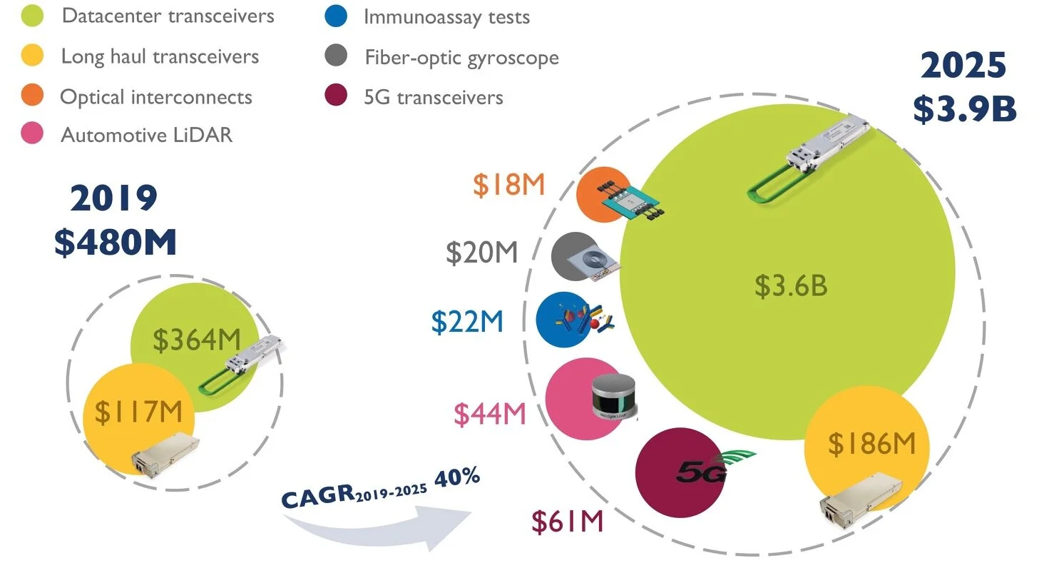
The market for silicon photonics is set to grow eightfold by 2025. So claims market research firm, Yole Développement, in its latest report on silicon photonics, a technology that enables optical components to be made on a silicon substrate.
Silicon photonics is also being used in new markets although optical transceivers will still account for the bulk of the revenues in 2025.
Source: Yole
Market forecast
“We are entering a phase where we are beyond the tipping point [for silicon photonics],” says Eric Mounier, fellow analyst at Yole. “There is no doubt silicon photonics will grow and will be used beyond the data centre.”
Yole sized the 2019 global silicon photonics market at US $480 million, dominated by sales of optical transceivers for the data centre. In 2025 the forecast is for a $3.9 billion market, with data centre transceivers accounting for over 90 per cent of the market.
Eric Mounier
Revenues from new markets such as 5G optical transceivers, automotive, co-packaged optics, fibre-optic gyroscopes, and biochemical sensors will generate $165 million revenues in 2025.
The Yole report also highlights a maturing supply chain, advances in co-packaged optics, and more silicon photonics start-up announcements in the last year.
“It seems the big data centre operators, telecom players and sensor companies are convinced silicon photonics is a key technology for integration, lower cost and smaller components for interconnect and sensing applications,” says Mounier.
Optical transceivers
Data centre optical transceivers account for the bulk of silicon photonics’ market value and unit volumes.
Three-quarters of revenues in 2019 were for data centre transceivers for reaches ranging from several hundred meters to 2km and 10km. This market for silicon photonics is dominated by two players: Intel and Cisco with its Luxtera acquisition.
“For 100-gigabit transceivers, silicon photonics is probably the most used technology compared to legacy optics,” says Mounier.
The remaining 2019 revenues were from long-haul coherent transceiver sales, a market dominated by Acacia that is being acquired by Cisco.
Other companies involved in the transceiver supply chain include Innolight, Juniper Networks, and Alibaba with its work with Elenion Technologies (Elenion was recently acquired by Nokia). HP is working with several firms to develop its silicon photonics supply chain, from device design to final products.
The rollout of 5G is generating a need for 10-gigabit and 25-gigabit transceivers for distances up to 100m, linking remote radio heads and the baseband unit, part of the 5G radio access network.
Yole forecasts a $61 million 5G transceiver market in 2025.
Co-packaged optics
The packaging of optical input-output with a digital chip, known as co-packaged optics, has made notable progress in the last year.
“We are pretty convinced that co-packaged optics is the next big application for silicon photonics,” says Mounier.
Intel has demonstrated its optics packaged with the Tofino 2 Ethernet switch chip it gained with the Barefoot Networks acquisition. “Talking to Intel, I believe in two to three years from now, there will be the first product,” he says.
Other firms pursuing co-packaged optics include Ranovus, Rockley Photonics, Ayar Labs and Sicoya.
The doubling in Ethernet switch-chip capacity every two years is a key driver for co-packaged optics. Switch chips with 25.6-terabit capacity exist and 51.2-terabit switches will be shipping by 2025.
There will also be eight-hundred-gigabit pluggable transceivers in 2025 but Yole says co-packaged optics offers a systems approach to increasing channel counts to keep pace with growing switch capacities.
Foundries and design houses
More than 10 foundries exist worldwide offering silicon photonics services.
“Foundries are interested in silicon photonics because they see a future opportunity for them to fill their fabs,” says Mounier.
Yole cites how GlobalFoundries is working with Ayar Labs, HP with TSMC, Sicoya with IHP Microelectronics, and Rockley Photonics with VTT Memsfab. TSMC also works with Cisco through its Luxtera acquisition.
Swedish MEMS foundry, Silex Microsystems, is developing a portfolio of silicon photonics technology. “They are working with many players developing telecom photonic platforms,” says Mounier.
There are also several design houses offering photonic design services to companies that want to bring products to market. Examples include VLC Photonics, Luceda, Photon Design and Effect Photonics.
Optical design requires know-how that not all firms have, says Mounier. Such silicon photonics design services recall the ASIC design houses that provided a similar service to the electronics industry some two decades ago.
Sensors
Lidar used for autonomous cars and biochemical chips are two emerging sensor markets embracing silicon photonics. Lidar (light detection and ranging) uses light to sense a vehicle’s surroundings.
“Lidar systems are bulky and expensive and a car needs several, at the front, rear and sides,” says Mounier. “Silicon photonics is an emerging platform for the integration of such devices.”
Two Lidar approaches are using silicon photonics: frequency modulation continuous wave (FMCW) Lidar, also known as coherent Lidar, and an optical phased array.
For coherent Lidar, the transmitted frequency of the laser - represented by the local oscillator - and the reflected signal are mixed coherently. This enables phase and amplitude information to be recovered to determine an object’s position and velocity.
SiLC Technologies has developed a FMCW Lidar chip. Working with Varroc Lighting Systems, the two firms have demonstrated Lidar integrated into a car headlamp.
The second approach - an optical phased array - steers the beam of light without using any moving parts.
Lidar is complex and can be implemented using other technologies besides silicon photonics, says Mounier: “Silicon photonics for Lidar has several advantages but it is not clear why the technology will be used in the car or for robotic vehicles.”
In turn, the emerging economic crisis worldwide will likely delay the development of the autonomous car, he says.
Other sensor developments include silicon photonics-based biosensors from Genalyte that use lasers, micro-ring resonators and detectors to produce fast biological test results. The US company has raised over $90 million in three rounds of funding.
French firm Aryballe produces a tiny photonic IC that acts as an electronic nose (digital olfaction). “Using silicon photonics, you can integrate everything on a chip,” says Mounier. “It needs less packaging and assembly and you get a tiny chip at the end.”
COVID-19
Silicon photonics shipments have been delayed in the first half of 2020 due to the COVID-19 pandemic, says Yole. But the market for silicon photonics will still grow this year albeit not at the originally forecasted 10 per cent.
“Everyone is working from home and there is a need for more networking bandwidth,” says Mounier. There will continued demand for transceivers for the data centre and telecom services.
“Market growth will be positive for telecoms, and markets such as defence and medical will not be much impacted,” he says.

Acacia bets on silicon as coherent enters its next phase
Gazettabyte interviewed Acacia Communications’ president and CEO, Murugesan ‘Raj’ Shanmugaraj, as the coherent technology company celebrates its 10th anniversary.

Raj Shanmugaraj
Acacia Communications has come a long way since Raj Shanmugaraj (pictured) first joined the company as CEO in early 2010. “It was just a few conference rooms and we didn't have enough chairs,” he says.
The company has since become a major optical coherent player with revenues of $340 million in 2018; revenues that would have been higher but for the four-month trade ban imposed by the US on Chinese equipment maker ZTE, an Acacia customer.
And as the market for coherent technology continues to grow, Acacia and other players are preparing for new opportunities.
“We are still in the early stages of the disruption," says Shanmugaraj. “You will see higher performance [coherent systems] in some parts of the network but there is going to be growth as coherent moves closer to the network edge.”
Here, lower power, flexibility and more integrated coherent solutions will be needed as the technology moves inside the data centre and closer to the network edge with the advent of 5G, higher-speed access and the Internet of Things (IoT).
Competitive landscape
Shanmugaraj prefers to focus on Acacia’s own strengths and products when asked about the growing competition in the coherent marketplace. However, recent developments present challenges for the company.
Systems vendors such as Huawei and Ciena are becoming more vertically integrated, developing not only their own coherent digital signal processor (DSP) ASICs but also optics. Ciena has also made its WaveLogic Ai DSP available to optical module makers Lumentum and NeoPhotonics and will sell its own optical modules using its latest WaveLogic 5 coherent silicon.
>
“You will see higher performance [coherent systems] in some parts of the network but there is going to be growth as coherent moves closer to the network edge ”
New coherent digital signal processor (DSP) players are also expected to enter the marketplace alongside established competitors, NEL and Inphi. The entrance of new players developing coherent DSPs is motivated by the unit volumes promised by 400ZR, the emerging 80km data centre interconnect interface standard.
“We are proponents of the fact that the merchant market will continue to grow, driven by interoperability and standardisation,” says Shanmugaraj. Such growth will lead to multiple markets where coherent technology will play. “There are going to be a few winners, not just one or two,” he says.
Acacia’s revenues were hit in 2018 following the US Department of Commerce’s enforced trade ban imposed on ZTE. However, the company recorded a strong fourth quarter posting revenues of $107 million, up almost a quarter on the revenues a year earlier. This followed strong ZTE orders after the ban was revoked.
Shanmugaraj says diversification has always been a priority for the company, independent of the trade issues between the US and China. The company has also been working to diversify its Chinese customer base. “So we are well positioned as these trade issues get resolved,” he says.
Origins
Acacia was established in mid-2009 by a core team from Mintera, a sub-system supplier that provided 40-gigabit DPSK line cards to network equipment suppliers. But Mintera folded and was eventually sold to Oclaro in July 2010.
Before joining Acacia, Shanmugaraj was at systems vendor Alcatel-Lucent where he learned two lessons.
One is that the long-term success of a company is based on technology leadership. “You want to be driven by technology or you fall behind your competitors,” he says. The second lesson was that the largest systems companies build products internally before an ecosystem becomes established, after which they buy from merchant suppliers.
This matched the vision of Acacia’s founders that sought to exploit their optical expertise gained at Mintera to become a leading merchant supplier of coherent transmission technology.
Stealth years
Acacia remained in secrecy for nearly half its existence, only revealing its technology and products in 2014 with the launch of the AC-100 CFP coherent pluggable module. The AC-100 is aimed at metro networks delivering a transmission reach of 80km to 1,200km. However, Acacia had already been selling 5x7-inch modules for 100-gigabit long-haul and ultra-long-haul applications as well as a 40-gigabit ultra-long-haul module.
“In the early years, there were just a few companies working on coherent,” says Shanmugaraj. “We had to be careful in terms of what products we were developing and what customers we were going after.”
Shanmugaraj says Acacia secured multi-million dollar commitments from customers even before it had a product. “It was the expertise of the founding team as well as the product concepts they were proposing that got them the commitments,” he says.
The backing enabled the company to manage with only $53 million of venture funding prior to its successful initial public offering in 2016.
“This was a pretty significant feat,” says Shanmugaraj. “Hardware start-ups, whether semiconductor or systems companies, use significantly more cash; these are expensive technologies to get off the ground.”
Shanmugaraj describes the early years as intense, with staff working between 60 and 70 hours a week.The then start-up had to be prudent with funding, not growing too quickly yet having sufficient resources to meet orders from systems customers that had their own orders to fulfil.
Coherent technologies
Acacia’s founders chose silicon for its coherent solutions, to replace ‘exotic materials’ such as indium phosphide and lithium niobate used in traditional optical transmission systems.
The company backed silicon photonics for the coherent optics, an industry trailblazing decision. To this aim, Acacia recruited Chris Doerr, the renowned optical integration specialist and Bell Labs Fellow.
The company also decided to develop its own coherent DSPs. By developing the optics and the DSP, Acacia could use a co-design approach when designing the hardware, trading off the performance of the optics and the signal processing to achieve an optimal design.
Shanmugaraj explains that the company chose a silicon-based approach to exploit the huge investment made by the semiconductor industry in chips and their packaging. Basing the components on silicon would not only simplify high-speed networks, he says, but it would also lower their power consumption and enable products to be made more quickly and cheaply.
“The beauty of silicon photonics is that it can be placed right next to a heat source, in this case, the high-power coherent DSP ASIC that generates a lot of heat,” says Shanmugaraj. “This allows for smaller form-factor designs.” In contrast, indium phosphide-based optics need to be temperature controlled when placed next to a hot chip, he says.
“Five or six years ago, people were challenging whether silicon photonics was even going to work at 100 and 200 gigabits,” says Shanmugaraj. Acacia has now used silicon photonics in all its products, including its latest high-end 1.2 terabits AC1200 coherent module.
Shanmugaraj sees Acacia's portfolio of coherent products as the company's biggest achievement: "You see start-ups that come out with one product that is a bestseller but we have continued to innovate and today we have a broad portfolio."
AC1200
The AC1200 module supports two optical wavelengths, each capable of supporting 100 to 600-gigabit transmissions in increments of 50 gigabits.
The AC1200 can be used for data centre interconnect links through to long distance submarine links. Acacia recently demonstrated the AC1200 transmitting a 400-gigabit signal over a 6,600km submarine cable.
“We are seeing strong interest in our AC1200 from network operators and expect our equipment customers to begin deployments this quarter,” says Shanmugaraj.
There are several reasons why network operators are choosing to deploy the AC1200, he says: “High capacity is important in data centre interconnect edge applications where we expect hyperscale operators may use the AC1200 in its full 1.2-terabit mode, but these applications are also sensitive to cost, power and density.”
The AC1200 also provides higher capacity in a smaller footprint than the 5x7-inch form factors currently available, he says, while for longer-reach applications, the AC1200 offers a combination of performance and flexibility that is setting the pace for the competition.
The data centre interconnect market represents a good opportunity for coherent interconnect suppliers because the operators drive and deploy technology at pace, says Shanmugaraj. Hyperscalers are continually looking to add more capacity in the same size and power constraints that exist today. Accordingly, this has been a priority development area for Acacia.
To increase capacity, companies have boosted the symbol rate from 32 gigabaud to 64 gigabaud while systems vendors Ciena and Infinera have recently detailed upcoming systems that support 800-gigabit wavelengths that use a symbol rate approaching 100 gigabaud.
The AC1200, which is due in systems in the coming quarter, demonstrates silicon photonics based modulation operating at up to 70 gigabaud while first indium-phosphide 800-gigabit per wavelength systems are due by the year-end.
“We don’t really see silicon photonics lagging behind indium phosphide,” says Shanmugaraj. “We think there is a path to even higher baud rates with silicon photonics, and 128 gigabaud is the next logical step up because it would double the data rate without needing to increase the modulation order.”
Higher modulation orders are also possible but the benefits must be weighed against increased complexity, he says.
400-gigabit coherent pluggables
Shanmugaraj says that the 400ZR pluggable module standard continues the trend to reduce the size and power consumption of optical transport systems in the data centre.
>
“You want to be driven by technology or you fall behind your competitors”
The current generation of data centre interconnect platforms, ranging from a 1 rack unit pizza box to a several rack-unit-sized chassis, were developed to be more compact than conventional optical transport platforms.
Now, with the advent of 400ZR that fits into a client-side QSFP-DD or OSFP module, data centre operators will be able to do away with such platforms for distances up to 80km by plugging the modules into the switch or router platforms and connecting them to open line systems.
“Costs come down because it [coherent] is getting down to the client-side form factors and that gives the hyperscalers more faceplate density,” says Shanmugaraj. “The hyperscalers also gain multi-vendor interoperability [with 400ZR] which is important as they want standardisation.”
Shanmugaraj admits that with the advent of 400ZR will bring greater competition. But he points out that the 400ZR is a complicated product to built that will challenge companies. Those players that have both the optics and a low-power DSP will have an advantage. “As long as it opens up the market wider, it is good for Acacia as it is in our control how we can win in the market,” says Shanmugaraj.
The industry expectation is that the 400ZR will start to be deployed in the second half of 2020.
There is also industry talk about 400ZR+, an interface that will be able to go beyond 80km that will require more advanced dispersion compensation and forward error correction schemes.
Shanmugaraj says it will be the same DSP ASIC that will support both the 400ZR and 400ZR+. However, a 400ZR+ interface will consume more power and so will likely require a larger module form factor than the ZR.
Meanwhile, the 400-gigabit CFP2-DCO pluggable for metro networks is built along the same lines as the 400ZR, says Shanmugaraj.
“Here you have applications like the Open ROADM MSA where network operators are trying to drive the same interoperability and not be stuck with one vendor,” he says. “This is driving the 400-gigabit evolution in the metro network for some of the largest telcos.”
There is also the open networking packet-optical opportunity, white-box platforms such as the Voyager and Cassini being developed by the Telecom Infra Project (TIP). Shanmugaraj says such white boxes rely on software solutions that are a work-in-progress and that much work is still to be done.
“The first generation showed that there is more work required to standardise the software and how that can be used by the hyperscalers,” he says. “It is an opportunity but we view it as more of a longer-term one.”
Emerging opportunities
The markets that are growing today are the metro, long haul, sub-sea and data centre interconnect, says Shanmugaraj.
The coherent applications that are emerging will result in products within the data centre as well as for 5G, access, the Internet of Things (IoT) and even autonomous vehicles.
Ultimately, what will lead to coherent being adopted within the data centre is the speed of the interfaces. “As you go to higher speeds, direct detection technology gets constrained [due to dispersion and other impairments],” says Shanmugaraj.
But for this to happen certain conditions will need to be met: the speed of interfaces on switches will need to increase, not just to 400 gigabits but 800 gigabits and greater.
“Looking to higher data rates beyond 400 gigabits, it gets more challenging for direct detect to achieve the necessary link budgets cost-effectively,” says Shanmugaraj. “It may be necessary to move from four-lane solutions to eight lanes in order to support the desired reaches. At the same time, we are working to make coherent more cost-effective for these applications.”
The other two conditions are the challenge of what form factors the coherent technology be squeezed into, andcost. Coherent optics is more expensive but its cost is driven by such factors as volumes, the level of automation that can be used to make the module, and the yield.
“There could be inflextion points where coherent becomes cost-competitive for some applications in the data centre,” says Shanmugaraj.
Companies will continue to innovate in both direct detect and coherent technologies and the market will determine the transition points. “But we do believe that coherent can be adopted inside data centres in the future,” he says.
In turn, metro and long-haul networks are already being upgraded in anticipation of 5G and the access requirements. “4G networks have a lot of 1-gigabit and 10-gigabit links but 5G has an order of magnitude higher throughput requirement,” says Shanmugaraj.
That means more capacity is needed for backhaul and that will lead to a proliferation of low-cost 100-gigabit coherent. A similar story is unfolding in access with the likes of the cable operators moving fibre closer to the network edge. This too will need low-cost 100-gigabit coherent interfaces.
IoT is a longer term opportunity and will be dependent on dense deployments of devices before the traffic will require sufficient aggregation to justify coherent.
“I don’t know if your refrigerator will have a coherent interface,” concludes Shanmugaraj. “But as you aggregated these [devices] into aggregation points, that becomes a driver for coherent at the edge.”

Data centre interconnect drives coherent
-
NeoPhotonics announced at OFC a high-speed modulator and intradyne coherent receiver (ICR) that support an 800-gigabit wavelength
-
It also announced limited availability of its nano integrable tunable laser assembly (nano-ITLA) and demonstrated its pico-ITLA, an even more compact silicon photonics-based laser assembly
-
The company also showcased a CFP2-DCO pluggable
NeoPhotonics unveiled several coherent optical transmission technologies at the OFC conference and exhibition held in San Diego last month.
“There are two [industry] thrusts going on right now: 400ZR and data centre interconnect pizza boxes going to even higher gigabits per wavelength,” says Ferris Lipscomb, vice president of marketing at NeoPhotonics.

Ferris Lipscomb
The 400ZR is an interoperable 400-gigabit coherent interface developed by the Optical Internetworking Forum (OIF).
Optical module makers are developing 400ZR solutions that fit within the client-side QSFP-DD and OSFP pluggable form factors, first samples of which are expected by year-end.
800-gigabit lambdas
Ciena and Infinera announced in the run-up to OFC their latest coherent systems - the WaveLogic 5 and ICE6, respectively - that will support 800-gigabit wavelengths. NeoPhotonics announced a micro intradyne coherent receiver (micro-ICR) and modulator components that are capable of supporting such 800-gigabit line-rate transmissions.
NeoPhotonics says its micro-ICR and coherent driver modulator are class 50 devices that support symbol rates of 85 to 90 gigabaud required for such a state-of-the-art line rate.
The OIF classification defines categories for devices based on their analogue bandwidth performance. “With class 20, the 3dB bandwidth of the receiver and the modulator is 20GHz,” says Lipscomb. “With tricks of the trade, you can make the symbol rate much higher than the 3dB bandwidth such that class 20 supports 32 gigabaud.” Thirty-two gigabaud is used for 100-gigabit and 200-gigabit coherent transmissions.
Class 50 refers to the highest component performance category where devices have an analogue bandwidth of 50GHz. This equates to a baud rate close to 100 gigabaud, fast enough to achieve data transmission rates exceeding a terabit. “But you have to allow for the overhead the forward-error correction takes, such that the usable data rate is less than the total,” says Lipscomb (see table).

Source: Gazettabyte, NeoPhotonics
Silicon photonics-based COSA
NeoPhotonics also announced a 64-gigabaud silicon photonics-based coherent optical subassembly (COSA). The COSA combines the receiver and modulator in a single package that is small enough to fit within a QSFP-DD or OSFP pluggable for applications such as 400ZR.
Last year, the company announced a similar COSA implemented in indium phosphide. In general, it is easier to do higher speed devices in indium phosphide, says Lipscomb, but while the performance in silicon photonics is not quite as good, it can be made good enough.
“It [silicon photonics] is now stretching certainly into the Class 40 [that supports 600-gigabit wavelengths] and there are indications, in certain circumstances, that you might be able to do it in the Class 50.”
Lipscomb says NeoPhotonics views silicon photonics as one more material that complements its indium phosphide, planar lightwave circuit and gallium arsenide technologies. “Our whole approach is that we use the material platform that is best for a certain application,” says Lipscomb.
In general, coherent products for telecom applications take time to ramp in volumes. “With the advent of data centre interconnect, the volume growth is much greater than it ever has been in the past,” says Lipscomb.
NeoPhotonics’ interested in silicon photonics is due to the manufacturing benefits it brings that help to scale volumes to meet the hyperscalers’ requirements. “Whereas indium phosphide has very good performance, the infrastructure is still limited and you can’t duplicate it overnight,” says Lipscomb. “That is what silicon photonics does, it gives you scale.”
NeoPhotonics also announced the limited availability of its nano integrable tunable laser assembly (nano-ITLA). “This is a version of our external cavity ITLA that has the narrowest line width in the industry,” says Lipscomb.
The nano-ITLA can be used as the source for Class 50, 800-gigabit systems and current Class 40 600 gigabit-per-wavelength systems. It is also small enough to fit within the QDFP-DD and OSFP client-side modules for 400ZR designs. “It is a new compact laser that can be used with all those speeds,” says Lipscomb.
NeoPhotonics also showed a silicon-photonics based pico-ITLA that is even smaller than the nano-ITLA.“The [nano-ITLA’s] optical cavity is now made using silicon photonics so that makes it a silicon photonics laser,” says Lipscomb.
Instead of having to assemble piece parts using silicon photonics, it can be made as one piece. “It means you can integrate that into the same chip you put your modulator and receiver on,” says Lipscomb. “So you can now put all three in a single COSA, what is called the IC-TROSA.” The IC-TROSA refers to an integrated coherent transmit-receive optical subassembly, defined by the OIF, that fits within the QSFP-DD and OSFP.
Despite the data centre interconnect market with its larger volumes and much faster product uptakes, indium phosphide will still be used in many places that require higher optical performance. “But for bulk high-volume applications, there are lots of advantages to silicon photonics,” says Lipscomb.
400ZR and 400ZR+
A key theme at this year’s OFC was the 80km 400ZR. Also of industry interest is the 400ZR+, not an OIF specification but an interface that extends the coherent range to metro distances.
Lipscomb says that the initial market for the 400ZR+ will be smaller than the 400ZR, while the ZR+’s optical performance will depend on how much power is left after the optics is squeezed into a QSFP-DD or OSFP module.
“The next generation of DSP will be required to have a power consumption low enough to do more than ZR distances,” he says. “The further you go, the more work the DSP has to do to eliminate the fibre impairments and therefore the more power it will consume.”
Will not the ZR+ curtail the market opportunity for the 400-gigabit CFP2-DCO that is also aimed at the metro?
“It’s a matter of timing,” says Lipscomb. “The advantage of the 400-gigabit CFP2-DCO is that you can almost do it now, whereas the ZR+ won’t be in volume till the end of 2020 or early 2021.”
Meanwhile, NeoPhotonics demonstrated at the show a CFP2-DCO capable of 100-gigabit and 200-gigabit transmissions.
NeoPhotonics has not detailed the merchant DSP it is using for its CFP2-DCO except to say that it working with ‘multiple ones’. This suggests it is using the merchant coherent DSPs from NEL and Inphi.
OFC interview regarding silicon photonics and our book
ADVA Optical Networking's Gareth Spence interviewed Daryl Inniss, director, new business development at OFS, and me at the OFC conference and exhibition held earlier this month in San Diego, California. We were interviewed regarding the status of silicon photonics and our book on the topic.

Click here for the interview.

Oclaro showcases its pluggable CFP2-DCO at ECOC
Multi-sourcing CFP2-DCO modules, coherent digital signal processor (DSP) partnerships, new laser opportunities and the latest on Lumentum’s acquisition of Oclaro. A conversation with Oclaro’s chief strategy officer, Yves LeMaitre.
Oclaro demonstrated its CFP2 Digital Coherent Optics (CFP2-DCO) pluggable module working with Acacia Communications’ own CFP2-DCO at the recent European Conference on Optical Communication (ECOC), held in Rome.
 Yves LeMaitreOclaro announced earlier this year that it would use Acacia’s Meru coherent DSP for a CFP2-DCO product.
The company also announced at ECOC the availability of a portfolio of single-mode lasers that operate over an extended temperature range.
“We see two new laser opportunities for us,” says LeMaitre. “The upgrade of the access networks and, concurrently, the deployment of 5G.”
Coherent pluggables
The CFP2-DCO is a dense wavelength-division multiplexing (DWDM) module that supports 100-gigabit and 200-gigabit data rates. With the CFP2-DCO design, the coherent DSP is integrated within the module, unlike the CFP2 Analog Coherent Optics (CFP2-ACO) where the DSP chip resides on the line card.
“A concern of the market is that there has been essentially only one source of CFP2-DCO for the last few years and it was Acacia,” says LeMaitre. “Now there will be a broader supply for people who want coherent pluggables.”
Oclaro has been selling a CFP2-ACO but the company could not address those systems vendors that do not have their own DSP yet want to use coherent pluggables. “Now we can leverage our optics and combine it with Acacia’s DSP and bring another source of the CFP2-DCO,” says LeMaitre.
Acacia’s Meru is a low-power DSP that supports 200 gigabit-per-second (Gbps) wavelengths using either 8-ary quadrature amplitude modulation (8-QAM) or 16-QAM. Using 8-QAM enhances the optical reach at 200 gigabit. Oclaro’s CFP2-DCO uses its indium phosphide-based optics whereas Acacia’s module uses the company’s silicon photonics technology.
Oclaro sees the deal with Acacia as a first step, given the coming generation of 400-gigabit coherent modules including the 400ZR.
Production of Oclaro’s CFP2-DCO will commence in early 2019.
WaveLogic Ai DSP
Oclaro, along with module makers Lumentum and NeoPhotonics, signed an agreement in 2017 with Ciena to use the equipment maker’s 400-gigabit WaveLogic Ai coherent DSP. Oclaro is now shipping the 400-gigabit optical module that uses the Ciena DSP.
“The market for these types of large 400-gigabit form-factor modules in fairly limited as it is already addressed by many of the network equipment manufacturers,” says LeMaitre. “It [the module] is targeted at a few customers and a few opportunities.”
When the agreement with the three module makers was announced, there was talk of Ciena developing coherent DSPs for emerging applications such as 400-gigabit pluggables. However, Ciena has since decided to bring its own coherent modules to the marketplace and Oclaro does not yet know if it will get access to Ciena’s future coherent DSPs.
“We remain very interested in working with Ciena if they give us access to a DSP that could fit into pluggable coherent solutions but we have no agreement on that,” says LeMaitre.
There is an expectation in terms of dollar-per-bit that 400-gigabit modules are not yet meeting
Access and 5G wireless
At ECOC, Oclaro announced the availability of extended-temperature 10-gigabit and 25-gigabit lasers for access network and 5G deployments. The company also detailed its electro-absorption modulated laser (EML) supporting single-wavelength 100-gigabit transmissions for the data centre.
LeMaitre says the latest laser opportunities stem from the expansion and speed upgrades of the access infrastructure as well as upcoming 5G deployments. “This is resulting in a new lease of life for single-mode lasers because of the faster speeds and increased distances,” he says. These distances range from 10-40km and even 80km.
The environmental conditions required for these applications means the lasers must operate over industrial temperature (I-Temp) ranges, from -40 to 85oC and even higher.
Oclaro’s 25-gigabit directly-modulated laser (DML) for 5G fronthaul and mid-haul applications operates at up to 95oC. This means the laser does not need a thermo-electric cooler, simplifying the module design and reducing its power consumption. The laser has also been operated at 50 gigabit-per-second (Gbps) using 4-level pulse-amplitude modulation (PAM-4).
LeMaitre says the architectures for 5G will vary depending on the density of deployments and the primary application such as broadband or the Internet of Things.
Oclaro also announced an extended temperature range DML for 10-gigabit passive optical networks such as XGS-PON and 10GE-PON. The laser, which operates at the 1270nm wavelength, is used at the optical network unit (ONU) at the premises. Oclaro is also developing new 10-gigabit EMLs for the downstream link, from the PON optical line terminal (OLT) to the ONU. Transmission distances for such PONs can be 20km.
The company recently expanded laser production at its Japan and UK facilities, while the 10- and 25-gigabit lasers are now being mass-produced.
400 Gigabit Ethernet
Oclaro was one of five companies that took part in a 100-gigabit single-wavelength interoperability demonstration organised by the Ethernet Alliance at the show. The other four were Applied Optoelectronics, InnoLight Technology, Source Photonics, and Sumitomo Electric Industries.
The company showed its EML operating at 50 gigabaud with PAM-4 in the 100-Gigabit QSFP28 module. The 50Gbaud EML can operate uncooled such that no thermo-electric cooler is needed.
Oclaro says it will soon start sampling a 400-gigabit QSFP-DD FR4 module. The 2km four-channel FR4 developed by the 100-Gigabit Single Lambda MSA will use four 50Gbaud lasers. Volume production of the FR4 module is expected from the second quarter of 2019.
LeMaitre says 400-gigabit modules for the data centre face two key challenges.
One is meeting the power consumption of the new form factor modules such as the QSFP-DD. The optics for a four-wavelength design consumes 3-4W while the accompanying PAM-4 digital signal processor can consume 7-8W. “A transceiver burning 10-12W might be an issue for large-scale deployments,” says LeMaitre. “There is a power issue here that needs to be fixed.”
The second challenge for 400-gigabit client-side is cost. The price of 100-gigabit modules has now come down considerably. “There is an expectation in terms of dollar-per-bit that 400-gigabit modules are not yet meeting,” says LeMaitre. If the DSPs have yet to meet the power needs while the cost of the new modules is not in line with the dollar-per-bit performance of 100-gigabit modules, then 400-gigabit modules will be delayed, he says.
Acquisition
Lumentum’s acquisition of Oclaro, announced in March, continues to progress.
LeMaitre says two of the main three hurdles have now been overcome: anti-trust clearance in the U.S. and gaining shareholder approval. What remains is achieving Chinese clearance via the State Authority for Market Regulation.
“Until the merger deal is closed, we have to continue to operate as two separate companies,” says LeMaitre. But that doesn't prevent the two firms planning for the day when the deal is completed. Issues being worked through include the new organisation, the geographic locations of the companies’ groups, and how the two firms will work together to build a combined financial model.
The deal is expected to close before the year-end.
Finisar demonstrates its first silicon photonics transceiver
- Finisar unveiled its first silicon photonics-based product, a 400-gigabit QSFP-DD DR4 module, at the recent ECOC event.
- The company also showed transceiver technology that simplifies the setting up of dense wavelength-division multiplexing (DWDM) links.
- Two 200-gigabit QSFP56 client-side modules and an extended reach 30km 400-gigabit eLR8 were also demonstrated by Finisar.
- A 64-gigabaud integrated tunable transmitter and receiver assembly (ITTRA) was used to send a 400-gigabit coherent wavelength.
Finisar is bringing to market its first silicon photonics-based optical module.
 Christian UrricarietThe 400GBASE-DR4 is an IEEE 500m-reach 400-gigabit parallel fibre standard based on four fibres, each carrying a 100-gigabit 4-level pulse amplitude modulation (PAM-4) signal. Finisar’s DR4 is integrated into a QSFP-DD module.
“The DR4 is the 400-gigabit interface that most of the hyperscale cloud players are interested in first,” says Christian Urricariet, senior director of global marketing at Finisar.
The company demonstrated the module at the recent European Conference on Optical Communication (ECOC), held in Rome.
Silicon photonics-based DR4
The DR4 is an integrated design, says Finisar, comprising modulators and photo-detectors as well as modulator drivers and the trans-impedance amplifiers (TIAs).
Finisar chose silicon photonics for the DR4 after undertaking an extensive technology study. Silicon photonics emerged as ‘a clear winner’ in terms of cost and performance for photonic designs made up of similar functions in parallel, such as the four-channel DR4. Silicon photonics manufacturing is also scalable, making it ideal for high-volume designs.
The DR4 is the 400-gigabit interface that most of the hyperscale cloud players are interested in first
The DR4 can also be used in a breakout mode to interface to four 100GBASE-DR modules. Also referred to as the DR1, the 100GBASE-DR fits within an SFP-DD or a QSFP28 module.
The DR4-DR1 combination can link four servers, each using a 100-gigabit link, to a 400-gigabit port on a top-of-rack or mid-row switch. The top-of-rack 400-gigabit DR4 can also connect to a leaf switch with multiple 100-gigabit ports. “The DR4 can be used ‘top-of-rack down’ [to servers] or ‘top-of-rack up’ [to leaf switches],” says Urricariet. “This is similar to what people are doing with the [100-gigabit parallel fibre] PSM4.”
400-gigabit eLR8
Finisar also showcased an extended reach version of the IEEE 400GBASE-LR8 standard.
Dubbed the eLR8, the QSFP-DD module is a technology demonstrator not a product that extends the reach of the LR8 from 10km to 30km.
Finisar already has an LR8 product in a CFP8 pluggable module and is moving the design to the smaller QSFP-DD. The LR8 is an eight-wavelength duplex interface where each wavelength carries a 50-gigabit PAM-4 signal.
“The 400GBASE-LR8 is a low-risk approach to achieving a 400-gigabit duplex single-mode link in the short term,” says Urricariet. “You don’t have to wait for 100-gigabit PAM-4 [ICs] to be manufactured in high volume.”
Urricariet says the IEEE is considering developing an extended LR8 standard with a 40km reach but such distances could also be addressed using inexpensive coherent technology.
Finisar’s design achieves the extended range using the same components as its LR8 module - directly modulated DFB lasers and PIN photodetectors. “There is plenty of margin with that [LR8 design],” says Urricariet. This suggests Finisar picked the best performing DFBs and PINs for the eLR8 design.
The QSFP-DD 10km LR8 design is sampling now, with general availability from the first half of 2019.
Flextune
Configuring DWDM links can be likened to two groups of people separated in a wood at night. Each individual has a flashlight and is tasked with finding a counterpart from the second group, a process repeated until everyone is paired.
Setting up DWDM links is comparable to telling each individual the exact path to take to find their counterpart. The Flextune technology that Finisar has developed can be viewed as giving each individual the confidence to stride out - sweeping their flashlights as they go - till they find a counterpart.
Currently, setting up a DWDM link requires coordination between a field engineer and network operations staff. Each tunable transceiver that is plugged into a port is told which wavelength to tune to. The system itself may tell the transceiver the wavelength to use or a field engineer programs each transceiver before it is plugged into the platform.
Equally, the transceiver output fibre must be connected to the right optical multiplexer and demultiplexer (mux-demux) port, as do the transceivers at the link’s other end.
The result is a time-consuming process that is prone to human error.
With Flextune, the tunable transceivers are plugged into the equipment’s ports and connected to the mux-demux’s ports. “It does not matter which port,” says Urricariet. “The transceivers search for each other and self-configure to the right wavelength.”
Each Flextune-enabled transceiver operates independently of the transceiver at the other end; there is no master-slave arrangement, says Urricariet, although a master-slave arrangement can be used if requested.
The mux-demux must also be a blocking architecture for Flextune to work. “If the mux-demux does not block the other wavelengths on each port, then you have a mess,” says Urricariet. With such a mux-demux, the channels scanned are blocked until the transceiver’s output is passed to the right channel. Once the link is established, the two transceivers set permanently to that wavelength.
“It [the process] happens at both ends simultaneously and on all the ports,” says Urricariet. “The basic technique can self-tune up to 96 [DWDM] channels in around five minutes.”
Being able to tune independently of the host equipment means that the Flextune-enabled transceivers can also be sold directly to operators and plugged into any of their equipment.
Urricariet says Flextune promises welcome operational savings given DWDM’s increasing adoption in the access network with developments such as 5G fronthaul.
The basic technique can self-tune up to 96 [DWDM] channels in around five minutes
Flextune will also be used for metro and data centre interconnect applications, as well as connecting Remote PHY nodes being deployed in cable networks. “The Remote PHY is also a big focus for this type of feature,” says Urricariet.
Finisar demonstrated Flextune with its 10-gigabit tunable SFP+ modules that are now sampling. Flextune will also be adopted for its 25-gigabit SFP+ that will sample ‘very soon’, followed by coherent modules.
“We do have a CFP2-ACO module in production and other coherent products on our roadmap,” says Urricariet. “We will be looking to implement Flextune technology in these products as well.”
Google has started deployments of 2x200GbE
200 Gigabit Ethernet: a growing interim solution
Finisar also demonstrated two 200-gigabit modules. The QSFP56 implements the 2km FR4 specification. The 200-gigabit FR4 uses four coarse WDM (CWDM) wavelengths, each carrying a 50-gigabit PAM-4 signal.
Finisar has previously said it will develop 200-gigabit modules for the large-scale data centres interested in the technology as an interim solution before 400-gigabit modules ramp. Such an intermediate market for “one hyperscaler and maybe two” is sufficient to justify making 200-gigabit modules, says Urricariet.
Market research firm LightCounting has increased its forecast for 200 Gigabit Ethernet (GbE) modules due to interest from Facebook.
A presentation by Facebook at ECOC suggested that 400 GbE is far from being ready, says Vladimir Kozlov, CEO of LightCounting. “It looks like 200GbE is being considered now, but Facebook may change its mind again,” says Kozlov. “In the meantime, Google has started deployments of 2x200GbE [in an OSFP module] as planned.”
As with the 400-gigabit eLR8, Finisar also demonstrated an extended reach version of the 200-gigabit FR4 to achieve a 10km reach. “This is not to be confused with the 10km 200-gigabit LR4 that is a LAN-WDM grid based design,” says Urricariet. “The extended FR4 uses a CWDM grid.”
ITTRA
At OFC 2018 in March, Finisar unveiled its 32-gigabaud (Gbaud) integrated tunable transmitter and receiver assembly (ITTRA) that combines the optics and electronics required for an analogue coherent optics interface.
The ITTRA comprises a tunable laser, an optical amplifier, modulators, modulator drivers, coherent mixers, a photo-detector array and the accompanying TIAs. All the components of the 32Gbaud ITTRA are integrated within a gold box that is 70 percent smaller than the size of a CFP2 module. The integrated assembly also has a power consumption below 7.5W.
At ECOC, the company demonstrated its second ITTRA design operating at 64Gbaud to transmit a 400-gigabit wavelength using 16-ary quadrature amplitude modulation (16-QAM). Finisar would not detail the power consumption of the 64Gbaud ITTRA.
“The doubling of the speed to 64Gbaud will enable 400-gigabit DCO modules as well as 400ZR,” says Urricariet. Digital coherent optics (DCO) refers to coherent modules that integrate the optics and the coherent digital signal processor (DSP).
Samples and production of the 64Gbaud ITTRA are due in 2019.
Intel targets 5G fronthaul with a 100G CWDM4 module
- Intel announced at ECOC that it is sampling a 10km extended temperature range 100-gigabit CWDM4 optical module for 5G fronthaul.
- Another announced pluggable module pursued by Intel is the 400 Gigabit Ethernet (GbE) parallel fibre DR4 standard.
- Intel, a backer of the CWDM8 MSA, says the 8-wavelength 400-gigabit module will not be in production before 2020.
Intel has expanded its portfolio of silicon photonics-based optical modules to address 5G mobile fronthaul and 400GbE.
 Robert BlumAt the European Conference on Optical Communication (ECOC) being held in Rome this week, Intel announced it is sampling a 100-gigabit CWDM4 module in a QSFP form factor for wireless fronthaul applications.
The CWDM4 module has an extended temperature range, -20°C to +85°C, and a 10km reach.
“The final samples are available now and [the product] will go into production in the first quarter of 2019,” says Robert Blum, director of strategic marketing and business development at Intel’s silicon photonics product division.
Intel also announced it will support the 400GBASE-DR4, the IEEE’s 400 GbE standard that uses four parallel fibres for transmit and four for the receive path, each carrying a 100-gigabit 4-level pulse amplitude modulation (PAM-4) signal.
5G wireless
5G wireless will be used for a variety of applications. Already this year the first 5G fixed and mobile wireless services are expected to be launched. 5G will also support massive Internet of Things (IoT) deployments as well as ultra-low latency applications.
The next-generation wireless standard uses new spectrum that includes millimetre wave spectrum in the 24GHz to 40GHz region. Such higher frequency bands will drive small-cell deployments.
5G’s use of new spectrum, small cells and advanced air interface techniques such as multiple input, multiple output (MIMO) antenna technology is what will enable its greater data speeds and vastly expanded capacity compared to the current LTE cellular standard.
 Source: Intel.
The 5G wireless standard will also drive greater fibre deployment at the network edge. And it is here where mobile fronthaul plays a role, linking the remote radio heads at the antennas with the centralised baseband controllers at the central office (see diagram). Such fronthaul links will use 25-gigabit and 100-gigabit links. “We have multiple customers that are excited about the 100-gigabit CWDM4 for these applications,” says Blum
Intel expects demand for 25-gigabit and 100-gigabit transceivers for mobile fronthaul to begin in 2019.
Intel is now producing over one million PSM4 and CWDM4 modules a year
Client-side modules
Intel entered the optical module market with its silicon photonics technology in 2016 with a 100-gigabit PSM4 module, quickly followed by a 100-gigabit CWDM4 module. Intel is now producing over one million PSM4 and CWDM4 modules a year.
Intel will provide customers with 400-gigabit DR4 samples in the final quarter of 2018 with production starting in the second half of 2019. This is when Intel says large-scale data centre operators will require 400 gigabits.
“The initial demand in hyperscale data centres for 400 gigabits will not be for duplex [fibre] but parallel fibre,” says Blum. “So we expect the DR4 to go to volume first and that is why we are announcing the product at ECOC.”
Intel says the advantages of its silicon photonics approach have already been demonstrated with its 100-gigabit PSM4 module. One is the optical performance resulting from the company’s heterogeneous integration technique combining indium-phosphide lasers with silicon photonics modulators on the one chip. Another advantage is scale using Intel’s 300mm wafer-scale manufacturing.
Intel says demand for the 500m-reach DR4 module to go hand-in-hand with that for the 100-gigabit single- wavelength DR1, given how the DR4 will also be used in breakout mode to interface with four DR1 modules.
“We don’t see the DR1 standard competing or replacing 100-gigabit CWDM4,” says Blum. “The 100-gigabit CWDM4 is now mature and at a very attractive price point.”
Intel is a leading proponent of the CWDM8 MSA, an optical module design based on eight wavelengths, each a 50 gigabit-per-second (Gbps) non-return-to-zero (NRZ) signal. The CWDM8 MSA was created to fast-track 400 gigabit interfaces by avoiding the wait for 100-gigabit PAM-4 silicon.
When the CWDM8 MSA was launched in 2017, the initial schedule was to deploy the module by the end of this year. Intel also demonstrated the module working at the OFC show held in March.
Now, Intel expects production of the CWDM8 in 2020 and, by then, other four-wavelength solutions using 100-gigabit PAM-4 silicon such as the 400G-FR4 MSA will be available.
“We just have to see what the use case will be and what the timing will be for the CWDM8’s deployment,” says Blum.
Imec eyes silicon photonics to solve chip I/O bottleneck
In the second and final article, the issue of adding optical input-output (I/O) to ICs is discussed with a focus on the work of the Imec nanoelectronics R&D centre that is using silicon photonics for optical I/O.
Part 2: Optical I/O
Imec has demonstrated a compact low-power silicon-photonics transceiver operating at 40 gigabits per second (Gbps). The silicon photonics transceiver design also uses 14nm FinFET CMOS technology to implement the accompanying driver and receiver electronics.
 Joris Van Campenhout“We wanted to develop an optical I/O technology that can interface to advanced CMOS technology,” says Joris Van Campenhout, director of the optical I/O R&D programme at Imec. “We want to directly stick our photonics device to that mainstream CMOS technology being used for advanced computing applications.”
Traditionally, the Belgium nanoelectronics R&D centre has focussed on scaling logic and memory but in 2010 it started an optical I/O research programme. “It was driven by the fact that we saw that electrical I/O doesn’t scale that well,” says Van Campenhout. Electrical interfaces have power, space and reach issues that get worse with each hike in transmission speed.
Imec is working with partner companies to research optical I/O. The players are not named but include semiconductor foundries, tool vendors, fabless chip companies and electronic design automation tools firms. The aim is to increase link capacity, bandwidth density - a measure of the link capacity that can be crammed in a given space - and reach using optical I/O. The research’s target is to achieve between a 10x to 100x in scaling.
The number of silicon photonics optical I/O circuits manufactured each year remains small, says Imec, several thousand to ten thousand semiconductor wafers at most. But Imec expects volumes to grow dramatically over the next five years as optical interconnects are used for ever shorter reaches, a few meters and eventually below one meter.
“That is why we are participating in this research, to put together building blocks to help in the technology pathfinding,” says Van Campenhout.
We wanted to develop an optical I/O technology that can interface to advanced CMOS technology
Silicon photonics transceiver
Imec has demonstrated a 1330nm optical transceiver operating at 40Gbps using non-return-to-zero signalling. The design uses hybrid integration to combine silicon photonics with 14nm FinFET CMOS electronics. The resulting transceiver occupies 0.025 mm2, the area across the combined silicon photonics and CMOS stack for a single transceiver channel. This equates to a bandwidth density of 1.6 terabit-per-second/mm2.
The silicon photonics and FinFET test chips each contain circuitry for eight transmit and eight receive channels. Combined, the transmitter path comprises a silicon photonics ring modulator and a FinFET differential driver while the receiver uses a germanium-based photo-detector and a first-stage FinFET trans-impedance amplifier (TIA).
The transceiver has an on-chip power consumption of 230 femtojoules-per-bit, although Van Campenhout stresses that this is a subset of the functionality needed for the complete link. “This number doesn’t include the off-chip laser power,” he says. “We still need to couple 13dBm - 20mW - of optical power in the silicon photonics chip to close the link budget.” Given the laser has an efficiency of 10 to 20 percent, that means another 100mW to 200mW of power.
That said, an equivalent speed electrical interface has an on-chip power consumption of some 2 picojoules-per-bit so the optical interface still has some margin to better the power efficiency of the equivalent electrical I/O. In turn, the optical I/O’s reach using single-mode fibre is several hundred meters, far greater than any electrical interface.
Imec is confident it can increase the optical interface’s speed to 56Gbps. The layout of the CMOS circuits can be improved to reduce internal parasitic capacitances while Imec has already improved the ring modulator design compared to the one used for the demonstrator.
“We believe that with a few design tweaks we can get to 56Gbps comfortably,” says Van Campenhout. “After that, to go faster will require new technology like PAM-4 rather than non-return-to-zero signalling.”
Imec has also tested four transmit channels using cascaded ring modulators on a common waveguide as part of work to add a wavelength-division multiplexing capability.
Transceiver packaging
The two devices - the silicon photonics die and the associated electronics - are combined using chip-stacking technology.
Both devices use micro-bumps with a 50-micron pitch with the FinFET die flip-chipped onto the silicon photonics die. The combined CMOS and silicon photonics assembly is glued on a test board and wire-bonded, while the v-groove fibre arrays are attached using active alignment. The fibre-to-chip coupling loss, at 4.5dB in the demonstration, remains high but the researchers say this can be reduced, having achieved 2dB coupling losses in separate test chips.
 Source: Imec.
Imec is also investigating using through-silicon vias (TSV) technology and a silicon photonics interposer in order to replace the wire-bonding. TSVs deliver better power and ground signals to the two dies and enable high-speed electrical I/O between the transceiver and the ASIC such as a switch chip. The optics and ASIC could be co-packaged or the transceiver used in an on-board optics design next to the chip.
“We have already shown the co-integration of TSVs with our own silicon photonics platform but we are not yet showing the integration with the CMOS die,” says Van Campenhout. “Something we are working on.”
Co-packaging the optics with silicon will come at a premium cost
Applications
The first ICs to adopt optical I/O will be used in the data centre and for high-performance computing. The latest data centre switch ICs, with a capacity of 12.8 terabits, are implemented using 16nm CMOS. Moving to a 7nm CMOS process node will enable capacities of 51.2 terabits. “These are the systems where the bandwidth density challenge is the largest,” says Van Campenhout.
But significant challenges must be overcome before this happens, he says: “I think we all agree that bringing optics deeply integrated into such a product is not a trivial thing.”
Co-packaging the optics with silicon will come at a premium cost. There are also reliability issues to be resolved and greater standardisation across the industry will be needed as to how the packaging should be done.
Van Campenhout expects this will only happen in the next four to five years, once the traffic-handling capacity of switch chips doubles and doubles again.
Imec has seen growing industry interest in optical I/O in the last two years. “We have a lot of active interactions so interest is accelerating now,” says Van Campenhout.