
Rockley Photonics showcases its in-packaged design at OFC
The packaged design includes Rockley's own 2 billion transistor layer 3 router chip, and its silicon photonics-based optical transceivers. The layer 3 router chip, described as a terabit device, also includes mixed-signal circuits needed for the optical transceevers' transmit and receive paths.
 Source: Rockley Photonics (annotated by Gazettabyte).
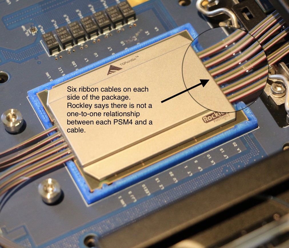
Rockley says it is using 500m-reach PSM4 transceivers for the design and that while a dozen ribbon cables are shown, this does not mean there are 12 100-gigabit PSM4 transceivers. The company is not saying what the total optical input-output is.
 Source: Rockley Photonics (annotated by Gazettabyte).
The company has said it is not looking to enter the marketplace as a switch chip player competing with the likes of Broadcom, Intel, Cavium, Barefoot Networks and Innovium. To develop such a device and remain competitive requires considerable investment and that is not Rockley's focus. Instead, it is using its router chip as a demonstrator to show the marketplace what can be done and that the technology works.
When asked what progress Rockley is making showcasing its technology, its CEO Andrew Rickman said: “It is going very well but nothing we can say publicly."
The switch chip makers continue to use electrical interfaces for their state-of-the-art switches which have a capacity of 12.8 terabits. It still remains to be seen which generation of switch chip will finally adopt in-packaged optics and whether on-board optics designs such as COBO will be adopted first.
For the full interview with CEO Andrew Rickman, click here.
Lumentum jolts the industry with Oclaro acquisition
Lumentum announced on Monday its plan to acquire Oclaro in a deal worth $1.8 billion.
The prospect of consolidation among optical component players has long been mooted yet the announcement provided the first big news jolt at the OFC show, being held in San Diego this week.
 Alan Lowe“Combined, we will be an industry leader in telecom transmission and transport as well as 3D sensing,” said Alan Lowe, president and CEO of Lumentum, on an analyst call discussing the deal.
Lumentum says their joint revenues totalled $1.7 billion with a 39% gross margin over the last year. And $60 million in synergies are forecast in the second year after the deal closes, which is expected to happen later this year.
The $1.8 billion acquisition will comprise 56 percent cash and 44 percent Lumentum stock. Lumentum will also raise $550 million to help finance the deal.
“This is a big deal as it consolidates the telecom part of the component market,” says Daryl Inniss, business development manager at OFS Fitel and former market research analyst.
Background
Lowe said that ever since Lumentum became a standalone company three years ago, the firm concentrated on addressing the increase in optical communications demand that started in late 2015 and then last year on ramping the production of its 3D sensing components. “Execution on major M&As had to wait,” he said.
The company investigated potential acquisitions and evaluated several key technologies including silicon photonics and indium phosphide. This led to it alighting on Oclaro with its indium phosphide and photonic integrated circuit (PIC) expertise.
Lowe also highlighted Oclaro’s strategy of the last five years of first trimming its business lines and then successfully executing on delivering optical transmission products.
Oclaro’s CEO, Greg Dougherty, CEO of Oclaro, described how his company has focussed on delivering differentiated photonic chip products to various growing end markets. “This is a very good combination for both companies and for the industry,” said Dougherty.
There is no overabundance in [optical] chip designers worldwide and together we have the strongest chip designer team in the world
Business plans
Lumentum’s business includes telecom transport components, modules and sub-systems. Its products include reconfigurable optical add/drop multiplexers (ROADMs), pump lasers, optical amplifiers and submarine products. In the second half of 2017, Lumentum’s telecom revenue mix was split three quarters telecom transport with transmission products accounted for the remaining quarter. Other Lumentum businesses include industrial lasers and 3D sensing.
In contrast, Oclaro’s focus in solely transmission components and modules, with the revenue mix in its most recent quarter being 53 percent telecom line side and 47 percent datacom client-side products.
The combined R&D resources of the merged company will allow it to do a much better job at supporting datacom products using the new QSFP-DD and OSFP form factors. “Right now I’m guessing that Alan is spread thin and I know the Oclaro datacom team has been spread thin,” says Dougherty.
The acquisition will also pool the two companies’ fabrication facilities.
Lumentum has already moved its lithium niobate manufacturing to its main gallium arsenide and indium phosphide fab in San Jose, California. San Jose also hosts a separate planar lightwave circuit fab.
Oclaro, which is headquartered in San Jose, has three photonic chip fabrication sites: an indium phosphide laser fab for datacom in Japan that makes directly modulated lasers (DMLs) and electro-absorption modulated lasers (EMLs), an indium phosphide fab in the UK that manufactures coherent optical components and sub-assemblies, and a lithium niobate fab in Italy.
The acquisition will also bolster the company’s chip design resources. “There is no overabundance in [optical] chip designers worldwide and together we have the strongest chip designer team in the world,” says Dougherty.
Lumentum plans to assign some of the chip designers to tackle a burgeoning pipeline of 3D sensing product designs.
In 2017 Lumentum reported three customers that accounted for nearly half of its revenues, while Oclaro had four customers, each accounted for 10 percent or more of its sales, in 4Q 2017. Oclaro selected customers include the webscale players, Amazon, Google and Microsoft, as well as leading systems vendors such as Ciena, Cisco, Coriant, Huawei, Juniper, Nokia and ZTE.
Both Oclaro and Lumentum, along with Neophotonics, signed an agreement with Ciena a year ago to use its WaveLogic Ai DSP in their coherent module designs.
Lumentum plans to provide more deal details closer to its closure. Meanwhile, the two CEOs will continue to run their companies with Oclaro’s Dougherty remaining at least during the transition period.
Further information:
For the link to the acquisition presentation, click here.
Rockley Photonics eyes multiple markets
Andrew Rickman, founder and CEO of silicon photonics start-up, Rockley Photonics, discusses the new joint venture with Hengtong Optic-Electric, the benefits of the company’s micron-wide optical waveguides and why the timing is right for silicon photonics.
 Andrew Rickman
The joint venture between Rockley Photonics and Chinese firm Hengtong Optic-Electric is the first announced example of Rockley’s business branching out.
The start-up’s focus has been to apply its silicon photonics know-how to data-centre applications. In particular, Rockley has developed an Opto-ASIC package that combines optical transceiver technology with its own switch chip design. Now it is using the transceiver technology for its joint venture.
“It was logical for us to carve out the pieces generated for the Opto-ASIC and additionally commercialise them in a standard transceiver format,” says Andrew Rickman, Rockley’s CEO. “That is what the joint venture is all about.”
Rockley is not stopping there. Rickman describes the start-up as a platform business, building silicon photonics and electronics chipsets for particular applications including markets other than telecom and datacom.
Joint venture
Hengtong and Rockley have set up the $42 million joint venture to make and sell optical transceivers.
Known for its optical fibre cables, Hengtong is also a maker of optical transceivers and owns 75.1 percent of the new joint venture. Rockley gains the remaining 24.9 percent share in return for giving Hengtong its 100-gigabit QSFP transceiver designs. The joint venture also becomes a customer of Rockley’s, buying its silicon photonics and electronics chips to make the QSFP modules.
“Hengtong is one of the world’s largest optical fibre cable manufacturers, is listed on the Shanghai stock market, and sells extensively in China and elsewhere into the data centre market,” says Rickman. “It is a great conduit, a great sales channel into these customers.”
The joint venture will make three 100-gigabit QSFP-based products: a PSM4 and a CWDM4 pluggable module and an active optical cable. Rickman expects the joint venture to make other module designs and points out that Rockley participates in the IEEE standards work for 400 gigabits and is one of the co-founders of the 400-gigabit CWDM8 MSA.
Rockley cites several reasons why the deal with Hengtong makes sense. First, a large part of the bill of materials used for active optical cables is the fibre itself, something which the vertically integrated Hengtong can provide.
China also has a ‘Made in China 2025’ initiative that encourages buying home-made optical modules. Teaming with Hengtong means Rockley can sell to the Chinese telecom operators and internet content players.
In addition, Hengtong is already doing substantial business with all of the global data centres as a cable, patch panel and connector supplier, says Rickman:“So it is an immediate sales channel into these companies without having to break into these businesses as a qualified supplier afresh.”
A huge amount of learning happened and then what Rockley represented was the opportunity to start all over again with a clean sheet of paper but with all that experience
Bigger is Best?
At the recent SPIE Photonics West conference held in San Francisco, Rickman gave a presentation entitled Silicon Photonics: Bigger is Better. His talk outlined the advantages of Rockley’s use of three-micron-wide optical waveguides, bucking the industry trend of using relatively advanced CMOS processes to make silicon photonics components.
Rickman describes as seductive the idea of using 45nm CMOS for optical waveguides.“These things exist and work but people are thinking of them in the same physics that have driven microelectronics,” he says. Moving to ever-smaller feature sizes may have driven Moore’s Law but using waveguide dimensions that are smaller than the wavelength of light makes things trickier.
To make his point, he plots the effective index of a waveguide against its size in microns. The effective index is a unitless measure - a ratio of a phase delay in a unit length of a waveguide relative to the phase delay in a vacuum. “Once you get below one micron, you get a waveguide that is highly polarisation-dependent and just a small variation in the size of the waveguide has a huge variation in the effective index,” says Rickman.
Such variations translate to inaccuracies in the operating wavelength. This impacts the accuracy of circuits, for example, arrayed-waveguide gratings built using waveguides to multiplex and demultiplex light for wavelength-division multiplexing (WDM).
“Above one micron is where you want to operate, where you can manufacture with a few percent variation in the width and height of a waveguide,” says Rickman.“But the minute you go below one micron, in order to hit the wavelength registration that you need for WDM, you have got to control the [waveguide’s] film thickness and line thickness to fractions of a percent.” A level of accuracy that the semiconductor industry cannot match, he says.
A 100GHz WDM channel equates to 0.8nm when expressed using a wavelength scale. “In our technology, you can easily get a wavelength registration on a WDM grid of less than 0.1nm,” says Rickman. “Exactly the same manufacturing technology applied to smaller waveguides is 25 times worse - the variation is 2.5nm.”
Moreover, WDM technology is becoming increasingly important in the data centre. The 100-gigabit PSM4 uses a single wavelength, the CWDM4 uses four, while the newer CWDM8 MSA for 400 gigabit uses eight wavelengths. “In telecom, 90-plus wavelengths can be used; the same thing will come to pass in the years to come in data centre devices,” he says.
Rockley also claims it has a compact modulator that is 50 times smaller than competing modulators despite them being implemented using nanometer feature sizes.
We set out to generate a platform that would be pervasive across communications, new forms of advanced computing, optical signal processing and a whole range of sensor applications
Opto-ASIC reference design
Rockley’s first platform technology example is its Opto-ASIC reference design. The design integrates silicon photonics-based transceivers with an in-house 2 billion transistor switch chip all in one package. Rockley demonstrated the technology at OFC 2017.
“If you look around, this is something the industry says is going to happen but there isn't a single practical instantiation of it,” says Rickman who points out that, like the semiconductor industry, very often a reference design needs to be built to demonstrate the technology to customers.“So we built a complete reference design - it is called Topanga - an optical-packaged switch solution,” he says.
Despite developing a terabyte-class packet processor, Rockley does not intend to compete with the established switch-chip players. The investment needed to produce a leading edge device and remain relevant is simply too great, he says.
Rockley has demonstrated its in-package design to relevant companies. “It is going very well but nothing we can say publicly,” says Rickman.
New Markets
Rockley is also pursuing opportunities beyond telecom and datacom.
“We set out to generate a platform that would be pervasive across communications, new forms of advanced computing, optical signal processing and a whole range of sensor applications,” says Rickman.
Using silicon photonics for sensors is generating a lot of interest. “We see these markets starting to emerge and they are larger than the data centre and communications markets,” he says. “A lot of these things are not in the public domain so it is very difficult to report on.”
Moreover, the company’s believes its technology gives it an advantage for such applications. “When we look across the other application areas, we don’t see the small waveguide platforms being able to compete,” says Rickman. Such applications can use relatively high power levels that exceed what the smaller waveguides can handle.
Rockley is sequencing the markets it will address. “We’ve chosen an approach where we have looked at the best match of the platform to the best opportunities and put them in an order that makes sense,” says Rickman.
Rockley Photonics represent Rickman’s third effort to bring silicon photonics to the marketplace.Bookham Technology, the first company he founded, build different prototypes in several different areas but the market wasn't ready. In 2005 he joined start-up Kotura as a board member. “A huge amount of learning happened and then what Rockley represented was the opportunity to start all over again with a clean sheet of paper but with all that experience,” says Rickman.
Back in 2013, Rockley saw certain opportunities for its platform approach and what has happened since is that their maturity and relevance has increased dramatically.
“Like all things it is always down to timing,” says Rickman. “The market is vastly bigger and much more ready than it was in the Bookham days.”
Ayar Labs advances I/O and pens GlobalFoundries deal
Silicon photonics start-up, Ayar Labs, has entered into a strategic agreement with semiconductor foundry, GlobalFoundries.
 Alexandra Wright-GladsteinAyar Labs will provide GlobalFoundries with its optical input-output (I/O) technology. In return, the start-up will gain early access to the foundry’s 45nm CMOS process being tailored for silicon photonics.
GlobalFoundries has also made an investment in the start-up for an undisclosed fee.
“We gain, first and foremost, a close relationship with GlobalFoundries as we qualify our product for customers,” says Alexandra Wright-Gladstein, co-founder and CEO of Ayar Labs. “That will help us speed up availability of our product and have their weight of support behind us.”
Strategy
Ayar Labs is bringing to market technology developed by academics originally at MIT. The research group developed a way to manufacture silicon photonics components using a standard silicon-on-insulator (SOI) CMOS process. The research work resulted in a novel dual-core RISC-V microprocessor demonstrator that used optical I/O to send and receive data, work that was published in the Nature science journal in December 2015.
Ayar Labs is using its optical I/O technology to address the high-performance computing and data centre markets. The optical I/O reaches up to 2km, from chip-to-chip communications to linking equipment between the buildings of a large data centre.
The start-up will offer a die - chiplet - that can be integrated within a multi-chip module, as well as a high-capacity 3.2-terabit optical module.
“We are aggregating the capacity of 4, 8 or 16 pluggable transceivers into a single module to share the cost of production at such high data rates,” says Wright-Gladstein. “This makes us competitive [for applications] where a pluggable transceiver is not.” Offering a chiplet and a high-density optical module on a board will bring to the marketplace the benefits companies are looking for if they are to move from copper to optics, she says.
Ayar Labs will also license its technology. “Our goal is to create an ecosystem for optical I/O for chips,” says Wright-Gladstein.

Technology
Ayar Labs has been a customer of GlobalFoundries for several years, using its existing 45nm SOI CMOS process to make devices as part of the foundry’s multi-project wafer service. The start-up will use the same 45nm CMOS process to make its first product. The CEO points out that using an unmodified electronics process introduces tight design constraints; no new materials can be introduced or layer thicknesses modified.
The start-up will also support GlobalFoundries in the development of its 45nm CMOS process optimised for silicon photonics. “The new process is more geared to traditional applications of optics such as optical transceivers for longer-distance communications,” says Wright-Gladstein.
Our goal is to create an ecosystem for optical I/O for chips
The intellectual property of Ayar Labs includes a micro-ring resonator optical modulator that is tiny compared to a Mach-Zehnder modulator. An issue with a micro-ring resonator is its sensitivity to temperature and manufacturing variances. Ayar’s Labs ability to design the ring resonator using standard CMOS means control circuitry can be added to ensure the modulator’s stability.
Ayar Labs has advanced its technology since the publication of the 2015 Nature paper. It has changed the operating wavelength of its optics from 1180nm to the standard 1310nm. It has also increased the speed of optical transmission from 2.5 to 25 gigabits-per-second (Gbps). The start-up expects to be able to extend the data rate to 50Gbps and even 100Gbps using 4-level pulse-amplitude modulation (PAM-4). The company has already demonstrated PAM-4 technology working with its optics.
The company also has wavelength-division multiplexing technology, using 8 wavelengths on a fibre; the original microprocessor demonstrator used only one wavelength. “We have 8 [micro-resonator] rings that lock on the transmit side and 8 rings that lock on the receive side,” says Wright-Gladstein. The company expects to extend the number of working wavelengths to 16 and even 32.
“We believe this is the process of the future because it can scale,” she says.
A factor of 10
Wright-Gladstein says its technology delivers a tenfold improvement using several metrics when compared to copper interconnect.
Typically a 25Gbps electrical interface will occupy 1 mm2 of chip area whereas Ayar Labs can fit more - potentially much more - than 250Gbps. The use of WDM technology also means that the amount of data passing the chip’s edge is at least 10 times greater.
The energy efficiency for the I/O is also between 5 times and 20 times greater than copper
The latency - how long it takes a signal to arrive at the receiver from the transmitter - is also improved tenfold. The fastest electrical interfaces at 56Gbps that use PAM-4 require forward-error correction which adds 100ns to the latency. Sending light 3m between racks takes 10ns, a tenth of the time. And more wavelengths can be added rather than using PAM-4 to avoid adversely impacting latency. “That matters for HPC customers,” she says.
The energy efficiency for the I/O is also between 5 times and 20 times greater than copper.
Ayar Labs has also developed an integrated laser module that provides the light sources for its optical I/O. Multiple lasers are integrated on a single die and the module outputs several wavelengths of light on several fibres.
The start-up claims the overall optical I/O design is simplified as there is no attachment of laser dies to the silicon and there are no attached driver chips. The result is a die that is flip-chip-attached allowing the use of standard high-volume CMOS packaging techniques.
First samples are expected sometime this year, with general product availability starting in 2019.
Meanwhile, GlobalFoundries is expected to offer the optical I/O as part of its 45nm silicon photonics process library in 2019.
Elenion's coherent and fibre-to-the-server plans
- Elenion’s coherent chip - an integrated modulator-receiver assembly - is now generally available.
- The company has a silicon photonics design library that includes over 1,000 elements.
- Elenion is also developing an optical engine for client-side interfaces.
Elenion Technologies has given an update on its activities and strategy after announcing itself eight months ago. The silicon photonics-based specialist is backed by private equity firm, Marlin Equity Partners, which also owns systems vendor, Coriant. Elenion had already been active for two and a half years and shipping product when it emerged from its state of secrecy last December.
 Larry SchwerinElenion has since announced it is selling its telecom product, a coherent transceiver PIC, to Coriant and now other companies.
It has also progressed its optical engine design for the data centre that will soon be a product. Elenion has been working with Ethernet switch chip maker, Cavium, and data centre player, Microsoft, as part of its datacom work.
“We have moved forward,” says Larry Schwerin, the CEO of Elenion.
Coherent PIC
Elenion’s integrated modulator-receiver assembly is being used by Coriant for two CFP2 Analogue Coherent Optics (CFP2-ACO) modules as part of its Groove G30 platform.
The first is a short-reach CFP2-ACO for point-to-point 200-gigabit links that has a reach of at least 80km. The second is a high-performance CFP2-ACO that has a reach of up to 4,000km at 100 gigabits and 650km at 200 gigabits.
Schwerin says the company is now selling the coherent PIC to “a lot of people”. In addition to the CFP2-ACO, there is the Digital Coherent Optics (DCO) pluggable market where the PIC and the coherent digital signal processor (DSP) are integrated within the module. Examples include the CFP-DCO and the smaller CFP2-DCO which is now being designed into new systems. ADVA Optical Networking is using the CFP2-DCO for its Teraflex, as is its acquisition target MRV with its 200-gigabit coherent muxponder. Infinera’s latest XTM II platforms also use the CFP2-DCO.
We have got a library that has well over 1,000 elements
Using silicon photonics benefits the cost and performance of the coherent design, says Schwerin. The cost benefit is a result of optical integration. “You can look at it as a highly simplified supply chain,” says Schwerin. Coupling the electronics close to the optics also optimises overall performance.
Elenion is also targeting the line-card market for its coherent PIC. “This is one of the reasons why I wanted to stay out of the pluggable business,” says Schwerin. “There are a lot more customers out there if you stay out of pluggables because now you are selling an [optical] engine.”
The company is also developing a coherent PIC design that will support higher data rates such as 400- and 600-gigabit per lambda. “Without being too specific because we do remain stealthy, we have plans to support these applications,” says Schwerin.
Schwerin stresses that the real strength of the company is its design library used to develop its silicon photonics circuits. Elenion emerged out of a silicon photonics design-for-service company. “We have got a library that has well over 1,000 elements,” he says. Elenion says it can address custom design requests of companies using its design library.
Datacom
Elenion announced at the OFC show held in Los Angeles in March that it is working with Jabil AOC Technologies, a subsidiary of the manufacturing firm, Jabil Circuits. Elenion chose the contract manufacturer due to its ability to address both line-card and pluggable designs, the markets for its optical engines.
The two firms have also been working at the chip level on such issues as fibre attach, coupling the laser and adding the associated electronics. “We are trying to make the interface as elegant and streamlined as possible,” says Schwerin. “We have got initiatives underway so that you don't need these complex arrangements.”
Schwerin highlights the disparity between the unit volumes needed for the telecom and datacom markets. According to forecasts from market research firms, the overall coherent market is expected to grow to 800,000 and 1 million units a year by 2020. In contrast, the interfaces used inside one large-scale data centre can be up to 2 million. “To achieve rapid manufacturing and yield, you have got to simplify the process,” he says.
This is what Elenion is tackling. If 1,000 die can be made on a single silicon wafer, and knowing the interface volumes required and the yields, the total number of wafer runs can be determined. And it is the overall time taken from starting a wafer to the finished transceiver PIC output that Elenion is looking to shorten, says the CEO.
We ran that demo from 7 AM to 2 AM every day of the show
At OFC, Elenion hired a hotel suite near the convention centre to demonstrate its technologies to interested companies. One demonstration used its 25Gbps optical engine directly mounted on a Cavium QLogic network interface card (NIC) connecting a server to a high-capacity Cavium Xpliant Ethernet switch chip. The demo showed how 16 NICs could be connected to the switch chip for a total capacity of 400 gigabits. “No more direct-attached cables or active optical cables, literally fibre-to-the-server,” says Schwerin. “We ran that demo from 7 AM to 2 AM every day of the show.”
Elenion’s on-board optics design was based on the emerging Consortium of On-Board Optics (COBO) standard. “The Microsoft folks, we work with them closely, so obviously what we are doing follows their intent,” says Schwerin.
The optical engine will also support 56Gbps links when used with four-level pulse-amplitude modulation (PAM-4) and the company is even eyeing 100Gbps interfaces. For now, Elenion’s datacom optical engine remains a technical platform but a product will soon follow.
The company’s datacom work is also benefiting its telecom designs. “The platform technology that we use for datacom has now found its way into the coherent programme, especially around the packaging,” says Schwerin.
* The article was changed on July 25th to mention that Elenion's PIC is being used in two Coriant CFP-ACOs.
Silicon photonics: concerns but viable and still evolving
Blaine Bateman set himself an ambitious goal when he started researching the topic of silicon photonics. The president of the management consultancy, EAF LLC, wanted to answer some key questions for a broad audience, not just academics and researchers developing silicon photonics but executives working in data centres, telecom and IT.
The result is a 192-page report entitled Silicon Photonics: Business Situation Report, 59 pages alone being references. In contrast to traditional market research reports, there is also no forecast or company profiles.
 Blaine Bateman's risk meter for silicon photonics. Eleven key elements needed to deploy a silicon photonics solution were considered. And these were assessed from the perspective of various communities involved or impacted by the technology, from silicon providers to cloud-computing users. Source: EAF LLC.
“I thought it would be helpful to give people a business view,” says Bateman.
Bateman works with companies on strategy in such areas as antennas, wireless technologies and more recently analytics and machine learning. But a growing awareness of photonics made him want to research the topic. “I could see a convergence between the evolution of telecom switching centres to become more like data centres, and data centres starting to look more like telecoms,” he says.
The attraction of silicon photonics is that it is an emerging technology with wide applicability in communications.
Just watching entirely new technologies emerge and become commercially viable in the span of ten years; it is astonishing
“Silicon Photonics is a good topic to research and publish to help a broader community because it is highly technical,” says Bateman. “It is also a great case study, just watching entirely new technologies emerge and become commercially viable in the span of ten years; it is astonishing.”
Bateman spent two years conducting interviews and reading a vast number of academic papers and trade-press articles before publishing the report earlier this year.
 Blaine BatemanThe main near-term opportunity for silicon photonics he investigated is the data centre. Moreover, not just large-scale data centre players with an obvious need for cheaper optics to interconnect servers but also enterprises facing important decisions regarding their cloud-computing strategy.
“The view that I developed is that it is still very early,” he says. “The price points for a given performance [of optics] are significantly higher than a Facebook thinks they need to meet their long-term business perspectives.”
The price-performance figure commonly floated is one dollar per gigabit but current 100-gigabit pluggable modules, whether using indium phosphide or silicon photonics, are several times more costly than that.
This is an important issue for cloud providers and for enterprises determining their cloud strategy.
Do cloud provider invest money in silicon photonics technologies for their data centres or do they let others be early adopters and come in later when prices have dropped? Equally, an enterprise considering moving their business operations to the cloud is in a precarious position, says Bateman. “If you pick the wrong horse, you could be boxed into a level of price and performance, while you will have competitors starting with cloud providers that have a 30 to 50 percent price-performance advantage,” he says. “In my view, it will trickle all the way to the large consumers of cloud resources.”
Longer term, the market will resolve the relative success of silicon photonics versus traditional optics but, near term, companies have some expensive decisions to make. “The price curve is still in the early phase,” says Bateman. “It just hasn’t come down enough that it is an easy decision.”
Bateman’s advice to enterprises considering a potential cloud provider is to ask about its roadmap plans regarding the deployment of photonics.
Findings
To help understand the technology and business risks associated with silicon photonics, Bateman has created risk meters. These are intuitive graphics that show the status of the different elements making up silicon photonics and the issues involved when making silicon phonics devices. These include the light source, modulation method, formation of the waveguides, fibering the chip and fabrication plants.
“The reason the fab is such a high risk is that even though the idea was to leverage existing foundries, in truth it is very much new processes,” says Bateman. “There is also a limited number of fabs that can build these things.”
The report also includes a risk meter summarising the overall status of silicon photonics (see above).
Bateman says there are concerns regarding silicon photonics which people need to be aware of but stresses that it is a viable technology.
This is one of two main conclusions he highlights. Silicon photonics is not mature enough to be at a commodity price. Accordingly, taking a non-commodity or early adopter technology could damage a company’s business plan in terms of cost and performance.
The second takeaway is that for every single aspect of silicon photonics, much is still open. “One of the reasons I made all these lists in the report - and I studied research from all over the globe - is that I wanted to show the management level that silicon photonics is still emerging,” says Bateman.
China is focused on innovation now, and has formidable resources
This surprised him. When a new technology comes to market, it typically uses R&D developed decades earlier. “In this area, I was shocked by the huge amount of basic research this is still ongoing and more and more is being done every day,” says Bateman. “It is daunting; it is moving so fast.”
Another aspect that surprised him was the amount of research coming out of Asia and in particular China. “This is also something new, seeing original work in China and other parts of the world,” he says.
The stereotypical view that China is a source of cheap manufacturing but little in terms of innovation must change, he says. In the US, in particular, there is still a large body of people that think this way, says Bateman: “I feel they have their head in the sand - China is focused on innovation now, and has formidable resources.”
Meeting the many needs of data centre interconnect
High capacity. Density. Power efficiency. Client-side optical interface choices. Coherent transmission. Direct detection. Open line system. Just some of the requirements vendors must offer to compete in the data centre interconnect market.
“A key lesson learned from all our interactions over the years is that there is no one-size-fits-all solution,” says Jörg-Peter Elbers, senior vice president of advanced technology, standards and IPR at ADVA Optical Networking. “What is important is that you have a portfolio to give customers what they need.”
 Jörg-Peter Elbers
Teraflex
ADVA Optical Networking detailed its Teraflex, the latest addition to its CloudConnect family of data centre interconnect products, at the OFC show held in Los Angeles in March (see video).
The platform is designed to meet the demanding needs of the large-scale data centre operators that want high-capacity, compact platforms that are also power efficient.
A key lesson learned from all our interactions over the years is that there is no one-size-fits-all solution
Teraflex is a one-rack-unit (1RU) stackable chassis that supports three hot-pluggable 1.2-terabit modules or ‘sleds’. A sled supports two line-side wavelengths, each capable of coherent transmission at up to 600 gigabits-per-second (Gbps). Each sled’s front panel supports various client-side interface module options: 12 x 100-gigabit QSFPs, 3 x 400-gigabit QSFP-DDs and lower speed 10-gigabit and 40-gigabit modules using ADVA Optical Networking’s MicroMux technology.
“Building a product optimised only for 400-gigabit would not hit the market with the right feature set,” says Elbers. “We need to give customers the possibility to address all the different scenarios in one competitive platform.”
The Teraflex achieves 600Gbps wavelengths using a 64-gigabaud symbol rate and 64-ary quadrature-amplitude modulation (64-QAM). ADVA Optical Networking is using Acacia’s Communications latest Pico dual-core coherent digital signal processor (DSP) to implement the 600-gigabit wavelengths. ADVA Optical Networking would not confirm Acacia is its supplier but Acacia decided to detail the Pico DSP at OFC because it wanted to end speculation as to the source of the coherent DSP for the Teraflex. That said, ADVA Optical Networking points out that Teraflex’s modular nature means coherent DSPs from various suppliers can be used.
 The 1 rack unit Teraflex
The line-side optics supports a variety of line speeds – from 600Gbps to 100Gbps, the lower the speed, the longer the reach.
The resulting 3-sled 1RU Teraflex platform thus supports up to 3.6 terabits-per-second (Tbps) of duplex communications. This compares to a maximum 800Gbps per rack unit using the current densest CloudConnect 0.5RU Quadflex card.
Markets
The data centre interconnect market is commonly split into metro and long haul.
The metro data centre interconnect market requires high-capacity, short-haul, point-to-point links up to 80km. Large-scale data centre operators may have several sites spread across a city, given they must pick locations where they can find them. Sites are typically no further apart than 80km to ensure a low-enough latency such that, collectively, they appear as one large logical data centre.
“You are extending the fabric inside the data centre across the data-centre boundary, which means the whole bandwidth you have on the fabric needs to be fed across the fibre link,” says Elbers. “If not, then there are bottlenecks and you are restricted in the flexibility you have.”
Large enterprises also use metro data centre interconnect. The enterprises’ businesses involve processing customer data - airline bookings, for example - and they cannot afford disruption. As a result, they may use twin data centres to ensure business continuity.
Here, too, latency is an issue especially if synchronous mirroring of data using Fibre Channel takes place between sites. The storage protocol requires acknowledgement between the end points such that the round-trip time over the fibre is critical. “The average distance of these connections is 40km, and no one wants to go beyond 80 or 100km,” says Elbers, who stresses that this is not an application for Teraflex given it is aimed at massive Ethernet transport. Customers using Fibre Channel typically need lower capacities and use more tailored solutions for the application.
The second data centre interconnect market - long haul - has different requirements. The links are long distance and the data sent between sites is limited to what is needed. Data centres are distributed to ensure continual business operation and for quality-of-experience by delivering services closer to customers.
Hundreds of gigabits and even terabits are sent over the long-distance links between data centres sites but commonly it is about a tenth of the data sent for metro data centre interconnect, says Elbers.
Direct Detection
Given the variety of customer requirements, ADVA Optical Networking is pursuing direct-detection line-side interfaces as well as coherent-based transmission.
At OFC, the system vendor detailed work with two proponents of line-side direct-detection technology - Inphi and Ranovus - as well as its coherent-based Teraflex announcement.
Working with Microsoft, Arista and Inphi, ADVA detailed a metro data centre interconnect demonstration that involved sending 4Tbps of data over an 80km link. The link comprised 40 Inphi ColorZ QSFP modules. A ColorZ module uses two wavelengths, each carrying 56Gbps using PAM-4 signalling. This is where having an open line system is important.
Microsoft wanted to use QSFPs directly in their switches rather than deploy additional transponders, says Elbers. But this still requires line amplification while the data centre operators want the same straightforward provisioning they expect with coherent technology. To this aim, ADVA demonstrated its SmartAmp technology that not only sets up the power levels of the wavelengths and provides optical amplification but also automatically measures and compensates for chromatic dispersion experienced over a link.
ADVA also detailed a 400Gbps metro transponder card based on PAM-4 implemented using two 200Gbps transmitter optical subassemblies (TOSAs) and two 200Gbps receiver optical subassemblies (ROSAs) from Ranovus.
Clearly there is also space for a direct-detection solution but that space will narrow down over time
Choices
The decision to use coherent or direct detection line-side optics boils down to a link’s requirements and the cost an end user is willing to pay, says Elbers.
As coherent-based optics has matured, it has migrated from long-haul to metro and now data centre interconnect. One way to cost-reduce coherent further is to cram more bits per transmission. “Teraflex is adding chunks of 1.2Tbps per sled which is great for people with very high capacities,” says Elbers, but small enterprises, for example, may only need a 100-gigabit link.
“For scenarios where you don’t need to have the highest spectral efficiency and the highest fibre capacity, you can get more cost-effective solutions,” says Elbers, explaining the system vendor’s interest in direct detection.
“We are seeing coherent penetrating more and more markets but still cost and power consumption are issues,” says Elbers. “Clearly there is also space for a direct-detection solution but that space will narrow down over time.”
Developments in silicon photonics that promise to reduce the cost of optics through greater integration and the adoption of packaging techniques from the CMOS industry will all help. “We are not there yet; this will require a couple of technology iterations,” says Elbers.
Until then, ADVA’s goal is for direct detection to cost half that of coherent.
“We want to have two technologies for the different areas; there needs to be a business justification [for using direct detection],” he says. “Having differentiated pricing between the two - coherent and direct detection - is clearly one element here.”
Coherent optics players target the network edge for growth
Part 1: Coherent developments
The market for optical links for reaches between 10km and 120km is emerging as a fierce battleground between proponents of coherent and direct-detection technologies.
Interest in higher data rates such as 400 gigabits is pushing coherent-based optical transmission from its traditional long-distance berth to shorter-reach applications. “That tends to be where the growth for coherent has come from as it has migrated from long-haul to metro,” says Tom Williams, senior director of marketing at Acacia Communications, a coherent technology supplier.
 Source: Acacia Communications, Gazettabyte
Williams points to the Optical Internetworking Forum’s (OIF) ongoing work to develop a 400-gigabit link for data centre interconnect. Dubbed 400ZR, the project is specifying an interoperable coherent interface that will support dense wavelength-division multiplexing (DWDM) links for distances of at least 80km.
Meanwhile, the IEEE standards group defining 400 Gigabit Ethernet has issued a Call-For-Interest to determine whether to form a Study Group to look at 400-Gigabit applications beyond the currently defined 10km 400GBASE-LR8 interface.
“Coherent moving to higher-volume, shorter-reach solutions shows it is not just a Cadillac product,” says Williams. Higher-volume markets will also be needed to fund coherent chip designs using advanced CMOS process nodes. “Seven nanometer [CMOS] becomes a very expensive prospect,” says Williams. “The traditional business case is not going to be there without finding higher volumes.”
Coherent moving to higher-volume, shorter-reach solutions shows it is not just a Cadillac product
Pico DSP
Acacia detailed its next-generation high-end coherent digital signal processor (DSP) at the OFC show held in Los Angeles in March.
 Tom WilliamsDubbed Pico, the DSP will support transmission speeds of up to 1.2 terabits-per-second using two carriers, each carrying 600 gigabits of data implemented using 64-ary quadrature amplitude modulation (64QAM) and a 64 gigabaud symbol rate. The 16nm CMOS dual-core DSP also features an internal crossbar switch to support a range of 100-gigabit and 400-gigabit client interfaces.
ADVA Optical Networking is using the Pico for its Teraflex data centre interconnect product. The Teraflex design supports 3.6 terabits of line-side capacity in a single rack unit (1RU). Each 1RU houses three “sleds”, each supporting two wavelengths operating at up to 600 gigabits-per-second (Gbps).
But ADVA Optical Networking also detailed at OFC its work with leading direct-detection technology proponents, Inphi and Ranovus. For the data centre interconnect market, there is interest in coherent and direct-detection technologies, says ADVA.
Detailing the Pico coherent DSP before it is launched as a product is a new development for Acacia. “We knew there would be speculation about ADVA’s Teraflex technology and we preferred to be up front about it,” says Williams.
The 16nm Pico chip was also linked to an Acacia post-deadline paper at OFC detailing the company’s progress in packaging its silicon photonics chips using ball grid array (BGA) technology. Williams stresses that process issues remain before its photonic integrated circuit (PIC) products will use BGA packaging, an approach that will simplify and reduce manufacturing costs.
“You are no longer running the board with all the electronics through a surface mount line and then have technicians manually solder on the optics,” says Williams. Moreover, BGA packaging will lead to greater signal integrity, an important consideration as the data rates between the coherent DSP and the PIC increase.
It is an endorsement of our model but I do not think it is the same as ours. You still have to have someone providing the DSP and someone else doing the optics
Coherent competition
Ciena's recent announcement that it is sharing its WaveLogic Ai coherent DSP technology with optical module vendors Lumentum, Oclaro and NeoPhotonics is seen as a response to Acacia’s success as a merchant supplier of coherent modules and coherent DSP technologies.
Williams says Acacia’s strategy remains the same when asked about the impact of the partnership between Ciena and the optical module makers: to continue being first to market with differentiated products.
One factor that has helped Acacia compete with merchant suppliers of coherent DSPs - NEL and ClariPhy, now acquired by Inphi - is that it also designs the silicon photonics-based optics used in its modules. This allows a trade-off between the DSP and the optics to benefit the overall system design.
A challenge facing the three optical module makers working with Ciena is that each one will have to go off and optimise their design, says Williams. “It is an endorsement of our model but I do not think it is the same as ours,” he says. “You still have to have someone providing the DSP and someone else doing the optics.”
Coherent roadmap
Acacia has managed to launch a new coherent DSP product every year since 2011 (see diagram, above). In 2015 it launched its Denali DSP, the first to operate at line rates greater than 100Gbps.
Last year it announced the Meru, a low-power DSP for its CFP2-DCO module. The CFP2-DCO operates at 100Gbps using polarisation multiplexing, quadrature phase-shift keying, (PM-QPSK) and two 200Gbps modes: one using 16-ary quadrature amplitude modulation (PM-16QAM) and a longer reach variant, implemented using a higher baud rate and 8-ary quadrature amplitude modulation (PM-8QAM). The CFP2-DCO is already starting to be designed into platforms.
Since 2014, Acacia has launched a low-power DSP design every even year and a high-end DSP every odd year, with the Pico being the latest example.
Acacia has not said when the Pico coherent DSP will be generally available but ADVA Optical Networking has said it expects to launch the Teraflex in early 2018.
Packaging silicon photonics using passive alignment
- An Israeli start-up is tackling a key packaging challenge for silicon photonics
Teramount has developed a way to simplify the packaging of silicon photonics chips. Instead of using active alignment whereby an external laser is required to carefully align a fibre to the optical die, the Israeli start-up has developed a technology that allows passive alignment.
 Hesham Taha“If we want silicon photonics to ramp up to volume, it has to meet CMOS standards both in terms of fabrication and packaging,” says Hesham Taha, Teramount's CEO.
Taha worked at a company developing atomic force microscopy systems before co-founding Teramount. "We got to know of the problem of injecting light into a waveguide and were surprised that the industry was still using active alignment," he says.
This spurred Taha and a colleague to develop optical solutions to match a single-mode fibre core to an optical waveguide, and they founded Teramount in Jerusalem in 2013. "We started real activity at the beginning of 2015 after getting funding," says Taha.
Existing silicon photonics companies either develop their own customised active alignment equipment or outsource the activity to a third party. "If we solve one of the bottlenecks of silicon photonics in terms of packaging, silicon photonics will be more and more adopted," says Taha.
If we want silicon photonics to ramp up to volume, it has to meet CMOS standards both in terms of fabrication and packaging
The design
Teramount's solution includes two elements: a PhotonicsPlug that is flip-chipped onto the silicon photonics die while still part of a wafer, and a 'bump', a design element added on the silicon photonics chip next to the optical waveguide. "Our solution, which we will be selling, is the PhotonicsPlug and we do require them [the designers] to add one element [the bump] to their silicon photonics chip," says Taha.
The main PhotonicsPlug component is a silicon die comprising optics that manipulates the beam using self-aligning optics and focusses it onto the silicon photonics chip via a glass spacer. Teramount’s die also has V-grooves to interface the single-mode ribbon fibre. Teramount says its die is made using an inexpensive mature CMOS process due to the relatively large feature sizes of the optical elements.
The second design element - the bump - is added next to the silicon photonics chip's grating coupler. The grating coupler is one of two techniques used in the industry to interface a fibre to the waveguide, the other being edge coupling.
“We want to place it [the bump] next to the waveguide so that the optics of the PhotonicPlug works in conjunction with it so that it brings the beam to the waveguide with a large tolerance,” says Taha. The bump is accurately placed on the chip using standard lithography techniques.
The resulting tolerance with which the die can be attached to the silicon photonics wafer is up to ± 20 microns in each of the three dimensions such that standard flip-chip machines can attach the PhotonicsPlug to the wafer.
“Flip-chip machines today work with a tolerance of ± 6 microns and can do 1,500 assemblies per hour,” says Taha.
"This is the main philosophy we are bringing here," he says. "Instead of the accurate placement of the fibre next to the grating coupler which requires active alignment, we want to replace that with a cheaper alignment technique that has much better accuracy at the wafer level," says Taha.
Status
Teramount has already shown working devices using the technology. In addition, Teramount is working with several partners and has demonstrated its technology with their silicon photonics chip designs. "With these partners we are doing the integration and qualifying the performance of the device," says Taha. "We will finalise at least two of these partnerships within a few months."
The start-up is also working to enable volume manufacturing by bringing its technology to industrial fabrication plants. This will be completed in the next few months.
Being a small start-up, the company is focussed on developing the grating coupler solution but it has already started work on an edge-coupling technique to a device’s waveguides. Edge coupling is suited to wavelength-division multiplexing (WDM) silicon photonics chips. That is because grating couplers are wavelength-dependent while edge coupling supports a broader range of wavelengths.
An insider's view on the merits of optical integration

Tolstikhin is president and CEO of Intengent, the Ottawa-based consultancy and custom design service provider, and an industry veteran of photonic integration. In 2005 he founded OneChip Photonics, a fabless maker of indium phosphide photonic integrated circuits for optical access.
One important lesson he learned at OneChip was how the cost benefit of a photonic integrated circuit (PIC) can be eroded with a cheap optical sub-assembly made from discrete off-the-shelf components. When OneChip started, the selling price for GPON optics was around $100 a unit but this quickly came down to $6. "We needed sales in volumes and they never came close to meeting $6," says Tolstikhin.
OneChip changed strategy, seeing early the emerging opportunity for 100-gigabit optics for the data centre but despite being among the first to demonstrate fully integrated 100-gigabit transmitter and receiver chips – at OFC 2013 – the company eventually folded.
When OneChip started, the selling price for GPON optics was around $100 a unit but this quickly came down to $6
Integent can be seen as the photonic equivalent of an electronic ASIC design house that was common in the chip industry, acting as the intermediary between an equipment vendor commissioning a chip design and the foundry making the chip.
Integent creates designs for system integrators which it takes to a commercial foundry for manufacturing. The company makes stand-alone devices, device arrays, and multi-function PICs. Integent uses the regrowth-free taper-assistant vertical integration (TAVI) indium phosphide process of the California-based foundry Global Communication Semiconductors (GCS). "We have also partnered with a prominent PIC design house, VLC Photonics, for PIC layout and verification testing,” says Tolstikhin. Together, Intengent, VLC and GCS offer a one-stop-shop for the development and production of PICs.
III-V and silicon photonics
Tolstikhin is a big fan of indium phosphide and related III-V semiconductor materials, pointing out that they can implement all the optical functions required for telecom and datacom applications. He is a firm believer that III-V will continue to be the material system of choice for various applications and argues that silicon photonics is not so much a competitor to III-V but a complement.
"Silicon photonics needs indium-phosphide-based sources but also benefits from III-V modulators and detectors, which have better performance than their silicon photonics counterparts," he says.
He admits that indium phosphide photonics cannot compete with the PIC scalability that silicon photonics offers. But that will benefit indium phosphide as silicon photonics matures. Intengent already benefits from this co-existence, offering specialised indium phosphide photonic chip development for silicon photonics as well.
"Silicon photonics cannot compete with indium phosphide photonics in relatively simple yet highest volume optical components for telecom and datacom transceivers," says Tolstikhin. Partly this is due to silicon photonics' performance inferiority but mainly for economical reasons.
Silicon photonics will have its chance, but only where it beats competing technologies on fundamentals, not just cost
There are also few applications that need monolithic photonic integration. Tolstikhin highlights coherent optics as one example but that is a market with limited volumes. Meanwhile, the most promising emerging market - transceivers for the data centre, whether 100-gigabit (4x25G NRZ) PSM or CWDM4 designs or in future 400-gigabit (4x100G PAM4) transceivers, will likely be implemented using optical sub-assembly and hybrid integration technologies.
Tolstikhin may be a proponent of indium phosphide but he does not dismiss silicon photonics' prospects: "It will have its chance, but only where it beats competing technologies on fundamentals, not just cost."
One such area is large-scale optoelectronic systems, such as data processors or switch fabrics for large-scale data centres. These are designs that cannot be assembled using discretes and go beyond the scalability of indium phosphide PICs. "This is not silicon photonics-based optical components instead of indium phosphide ones but a totally different system and possibly network solutions," he says. This is also where co-integration of CMOS electronics with silicon photonics makes a difference and can be justified economically.
He highlights Rockley Photonics and Ayar Labs as start-ups doing just this: using silicon photonics for large-scale electro-photonic integration targeting system and network applications. "There may also be more such companies in the making," says Tolstikhin. "And should they succeed, the entire setup of optics for the data centre and the role of silicon photonics could change quite dramatically."