
ECOC 2015 Review - Final Part
Part 2 - Client-side component and module developments
- The first SWDM Alliance module shown
- More companies detail CWDM4, CLR4 and PSM4 mid-reach modules
- 400 Gig datacom technologies showcased
- The CFP8 MSA for 400 Gigabit Ethernet unveiled
 The CFP MSA modules including the newest CFP8. Source: Finisar
- Lumentum and Kaiam use silicon photonics for mid-reach modules
- Finisar demonstrates a 10 km 25 Gig SFP28, and low-latency 25 Gig and 100 Gig SR4 interfaces
Shortwave wavelength-division multiplexing
Finisar demonstrated the first 100 gigabit shortwave wavelength-division multiplexing (SWDM) module at ECOC. Dubbed the SWDM4, the 100 gigabit interface supports WDM over multi-mode fibre. Finisar showed a 40 version at OFC earlier this year. “This product [the SWDM4] provides the next step in that upgrade path,” says Rafik Ward, vice president of marketing at Finisar.
The SWDM Alliance was formed in September to exploit the large amount of multi-mode fibre used by enterprises. The goal of the SWDM Alliance is to extend the use of multi-mode fibre by enabling link speeds beyond 10 gigabit.
“We believe if you can do something with multi-mode fibre, you can achieve cost points that are not achievable with single-mode fibre,” says Ward. “SWDM4 allows us to have not only low-cost optics on either end, but allows customers to reuse their installed fibre.”
The SWDM4 interface uses four 25 gigabit VCSELs operating at wavelengths sufficiently apart that cooling is not required. “By having this [wavelength] gap, you can keep to relatively low-cost components like for multiplexing and de-multiplexing,” says Ward.
The 100 Gig SWDM4 achieves 70 meters over OM3 fibre and 100 meters over OM4 fibre. SWDM can scale beyond 100 gigabit, says Ward, but the challenge with multi-mode fibre remains the tradeoff between speed and distance.
Finisar is already shipping SWDM4 alpha samples to customers.
The SWDM Alliance founding members include CommScope, Corning, Dell, Finisar, H3C, Huawei, Juniper Networks, Lumentum, and OFS.
CWDM4, CLR4 and PSM4
Oclaro detailed a 100 gigabit mid-reach QSFP28 module that supports both the CWDM4 multi-source agreement (MSA) and the CLR4 MSA. “We can support either depending on whether, on the host card, there is forward-error correction or not,” says Robert Blum, director of strategic marketing at Oclaro.
Both MSAs have a 2 km reach and use four 25 gigabit channels. However, the CWDM4 uses a more relaxed optical specification as its overall performance is complemented with forward-error correction (FEC) on the host card. The CLR4, in contrast, does not use FEC and therefore requires a more demanding optical specification.
“The requirements are significantly harder to meet for the CLR4 specification,” says Blum. By avoiding FEC, the CLR4 module benefits low-latency applications such as financial trading.
Oclaro showed its dual-MSA module achieving a 10 km reach at ECOC even though the two specifications call for 2 km only. “We have very large margins for the module compared to the specification,” says Blum, adding that customers now need to only qualify one module to meet their CWDM4 or CLR4 line card needs.
Other optical module vendors that announced support for CWDM4 in a QSFP28 module include Source Photonics, whose module is also CLR4-compliant. Kaiam is making CWDM4 and CLR4 modules using silicon photonics as part of its designs.
Lumentum also detailed its CWDM4 and the PSM4, a QSFP28 that uses a single-mode ribbon cable to deliver 100 Gig over 500 meters. Lumentum says its CWDM4 and PSM4 QSFP28 products will be available this quarter. “These 100 gigabit modules are what the hyper-scale data centre operators are clamouring for,” says Brandon Collings, CTO of Lumentum.
The question is who can ramp and support the 100 Gig deployments that are going to happen next year
Lumentum says it is using silicon photonics technology for one of its designs but has not said which. “We have both technologies [indium phosphide and silicon photonics], we use both technologies, and silicon photonics is involved with one of these [modules],” says Collings.
There is demand for both the PSM4 and CWDM4, says Lumentum. Which type a particular data centre operator chooses depends on such factors as what fibre they have or plan to deploy, whether they favour single-mode fibre pairs or ribbon cable, and if their reach requirements are beyond 500 meters.
Quite a few module companies have already sampled [100 Gig] products, says Oclaro’s Blum: “The question is who can ramp and support the 100 Gig deployments that are going to happen next year.”
Technologies for 400 gigabit
Several companies demonstrated technologies that will be needed for 400 gigabit client-side interfaces.
NeoPhotonics and chip company InPhi partnered to demonstrate the use of PAM-4 modulation to achieve 100 gigabit. “To do PAM-4, you need not only the optics but a special PAM-4 DSP,” says Ferris Lipscomb, vice president of marketing at NeoPhotonics.
The 400 Gigabit Ethernet standard under development by the IEEE 802.3bs supports several configurations using PAM-4 including a four-channel parallel single-mode fibre configuration, each at 100 gigabit that will have a 500m reach, and two 8 x 50 gigabit, for 2 km and 10 km links.
The company showcased its 4x28 Gig transmitter optical sub-assembly (TOSA) that uses a photonic integrated circuit comprising electro-absorptive modulated lasers (EMLs). Combined with InPhi’s PAM-4 chip, two channels were combined to achieve 100 gigabit. NeoPhotonics says its EMLs are also capable of supporting 56 gigabaud rates which, coupled with PAM-4, would achieve 100 gigabit single channels.
Lipscomb points out that not only are there several interfaces under development but also various optical form factors. “For 100 Gig and 400 Gig client-side data centre links, there are several competing MSA groups,” says Lipscomb. “The final winning approach has not yet emerged and NeoPhotonics wants its solution to be generic enough so that it supports this winning approach once it emerges.”
Meanwhile, Teraxion announced its silicon photonics-based modulator technology for 100 gigabit (4 x 25 Gig) and 400 gigabit datacom interfaces. “People we talk to are interested in WDM applications for short-reach links,” says Martin Guy, Teraxion’s CTO and strategic marketing.
Teraxion says a challenge using silicon photonics for WDM is supporting a broad band of wavelengths. “People use surface gratings to couple light into the silicon photonics,” says Guy. “But surface gratings have a strong wavelength-dependency over the C-band.”
Teraxion has developed an edge coupler instead which is on the same plane as the propagating light. This compares to a surface grating where light is coupled vertical to the plane.
You hear a lot about the cost of silicon photonics but one of the key advantages is the density you can achieve on the chip itself. Having many modulators in a very small footprint has value for the platform; you can make smaller and smaller transceivers.
“We can couple light efficiently with large-tolerance alignment and our approach can be used for WDM applications,” says Guy. Teraxion’s modulator array can be used for CWDM4 and CLR4 MSAs as well as optical engines for future 400 gigabit datacom systems.
“You hear a lot about the cost of silicon photonics but one of the key advantages is the density you can achieve on the chip itself,” says Guy. “Having many modulators in a very small footprint has value for the platform; you can make smaller and smaller transceivers.”
CFP8 MSA
Finisar demonstrated a 400 gigabit link that included a mock-up of the CFP8 form factor, the latest CFP MSA member being developed to support emerging standards such as 400 Gigabit Ethernet.
The 400 gigabit demonstration implemented the 400GE-SR16 multi-mode standard. A Xilinx FPGA was used to implement an Ethernet MAC and generated 16, 25 Gig channels that were fed to four CFP4 modules, each implementing a 100GBASE-SR4 but collectively acting as the equivalent of the 400GE-SR16. The 16 fibre outputs were then fed to the CFP8 prototype which performed an optical loop-back function, sending the signals back to the CFP4s and FPGA.

The CFP8 will be able to support 6.4 terabit of switching on a 1U card when used in a 2 row by 8 module configuration. The CFP8 has a similar size and power consumption profile of the CFP2. “There is still a lot of work putting an MSA together for 400 gigabit,” says Ward, adding that there is still no timeframe as to when the CFP8 MSA will be completed.
25 Gig SFP28
Finisar also announced at ECOC a 1310nm SFP28 supporting 25 gigabit Ethernet over 10 km, complementing the 850nm SFP28 short reach module it announced at OFC 2015.
Ethernet vendors are designing their next-generation series of switches that use the SFP28, says Finisar, while the IEEE is completing standardising 25 Gigabit Rthernet over copper and multi-mode fibre options.
“There hasn’t yet been a motion to standardise a long-wave interface,” says Ward. “With the demo at ECOC, we have come out with a 25 Gig long-wave interface in advance of a standard.”
Ward points out that the large-scale data centres several years ago only had 40 gigabit as a higher speed option beyond 10 gigabit. Now enterprises will also have a 25 gigabit option.
Ward points out that 25 gigabit compared to 40 Gig delivers an attractive cost-performance. Forty gigabit short-reach and long-reach interfaces are based on four channels at 10 gigabit, whereas 25 gigabit uses one laser and one photo-detector that fit in an SFP28. This compares to a QSFP for 40 Gig.
“25 Gigabit Ethernet is a very interesting interface for the next set of customers after the Web 2.0 players that are looking to migrate beyond 10 gigabit,” said Ward.
Low-latency 25 Gig SR and 100 Gig Ethernet SR4 modules
Also announced by Finisar are 25 Gigabit Ethernet SFP28 SR and 100GE QSFP28 SR4 transceivers that can operate without accompanying FEC on the host board. The transceivers achieve a 30 meter reach on OM3 fibre and 40 meters using OM4 fibre.
“Using FEC simplifies the optical link,” says Ward. “It can take the cost out of the optics by having FEC which gives you additional gain.” But some customers have requested the parts for use without FEC to reduce link latency, similar to those that choose the CLR4 MSA for mid-reach 100 Gig.
Finisar has not redesigned its modules but offering modules that have its higher performing VCSELs and photo-detectors. “Think of it as a simple screen,” says Ward.
Click here for the ECOC 2015 Review - Part 1.
ECOC '15 Reflections: Part 2
Martin Zirngibl, head of network enabling components and technologies at Bell Labs.
Silicon Photonics is seeming to gain traction, but traditional component suppliers are still betting on indium phosphide.
There are many new start-ups in silicon photonics, most seem to be going after the 100 gigabit QSFP28 market. However, silicon photonics still needs a ubiquitous high-volume application for the foundry model to be sustainable.
There is a battle between 4x25 Gig CWDM and 100 Gig PAM-4 56 gigabaud, with most people believing that 400 Gig PAM-4 or discrete multi-tone with 100 Gig per lambda will win.
Will coherent make it into black and white applications - up to 80 km - or is there a role for a low-cost wavelength-division multiplexing (WDM) system with direct detection?
One highlight at ECOC was the 3D integrated 100 Gig silicon photonics by Kaiam.
In coherent, the analogue coherent optics (ACO) model seems to be winning over the digital coherent one, and people are now talking about 400 Gig single carrier for metro and data centre interconnect applications.
As for what I’ll track in the coming year: will coherent make it into black and white applications - up to 80 km - or is there a role for a low-cost wavelength-division multiplexing (WDM) system with direct detection?
Yukiharu Fuse, director, marketing department at Fujitsu Optical Components
There were no real surprises as such at ECOC this year. The products and demonstrations on show were within expectations but perhaps were more realistic than last year’s show.
Most of the optical component suppliers demonstrated support to meet the increasing demand of data centres for optical interfaces.
The CFP2 Analogue Coherent Optics (CFP2-ACO) form factor’s ability to support multiple modulation formats configurable by the user makes it a popular choice for data centre interconnect applications. In particular, by supporting 16-QAM, the CFP2-ACO can double the link capacity using the same optics.
Lithium niobate and indium-phosphide modulators will continue to be needed for coherent optical transmission for years to come
Recent developments in indium phosphide designs has helped realise the compact packaging needed to fit within the CFP2 form factor.
I saw the level of integration and optical engine configurations within the CFP2-ACO differ from vendor to vendor. I’m interested to see which approach ends up being the most economical once volume production starts.
Oclaro introduced a high-bandwidth lithium niobate modulator for single wavelength 400 gigabit optical transmission. Lithium niobate continues to play an important role in enabling future higher baud rate applications with its excellent bandwidth performance. My belief is that both lithium niobate and indium-phosphide modulators will continue to be needed for coherent optical transmission for years to come.
Chris Cole, senior director, transceiver engineering at Finisar
ECOC technical sessions and exhibition used to be dominated by telecom and long haul transport technology. There is a shift to a much greater percentage focused on datacom and data centre technology.
What I learned at the show is that cost pressures are increasing
There were no major surprises at the show. It was interesting to see about half of the exhibition floor occupied by Chinese optics suppliers funded by several Chinese government entities like municipalities jump-starting industrial development.
What I learned at the show is that cost pressures are increasing.
New datacom optics technologies including optical packaging, thermal management, indium phosphide and silicon integration are all on the agenda to track in the coming year.
ECOC 2015: Reflections
Valery Tolstikhin, head of a design consultancy, Intengent

ECOC was a big show and included a number of satellite events, such as the 6th European Forum on Photonic Integration, the 3rd Optical Interconnect in Data Center Symposium and Market Focus, all of which I attended. So, lots of information to digest.
My focus was mainly on data centre optical interconnects and photonic integration.
Data centre interconnects
What became evident at ECOC is that 50 Gig modulation and the PAM-4 modulation format will be the basis of the next generation (after 100 Gig) data centre interconnect. This is in contrast to the current 100 Gig non-return-to-zero (NRZ) modulation using 25 Gig lanes.
This paves the way towards 200 Gig (4 x PAM-4 lanes at 25 Gig) and 400 Gig (4 x PAM-4 lanes at 50 Gig) as a continuation of quads of 4 x NRZ lanes at 25 Gig, the state-of-the-art data centre interconnect still to take off in terms of practical deployment.
The transition from 100 Gig to 400 Gig seems to be happening much faster than from 40Gig to 100 Gig. And 40 Gig serial finally seems to have gone; who needs 40 Gig when 50 Gig is available?
Another observation is that despite the common agreement that future new deployments should use single-mode fibre rather than multi-mode fibre, given the latter’s severe reach limitation that worsens with modulation speed, the multi-mode fibre camp does not give up easily.
That is because of the tons of multi-mode fibre interconnects already deployed, and the low cost of gallium arsenide 850 nm VCSELs these links use. However, the spectral efficiency of such interconnects is low, resulting in high multi-mode fibre count and the associated cost. This is a strong argument against such fibre.
Now, a short-wave WDM (SWDM) initiative is emerging as a partial solution to this problem, led by Finisar. Both OM3 and OM4 multi-mode fibre can be used, extending link spans to 100m at 25 Gig speeds.
Single mode fibre 4 x 25 Gig QSFP28 pluggables with a reach of up to 2 km, which a year ago were announced with some fanfare, seems to have become more of a commodity.
The SWDM Alliance was announced just before ECOC 2015, with major players like Finisar and Corning on board, suggesting this is a serious effort not to be ignored by the single mode fibre camp.
Lastly, single mode fibre 4 x 25 Gig QSFP28 pluggables with a reach of up to 2 km, which a year ago were announced with some fanfare, seems to have become more of a commodity. Two major varieties – PSM and WDM – are claimed and, probably shipping, by a growing number of vendors.
Since these are pluggables with fixed specs, the only difference from the customer viewpoint is price. That suggests a price war is looming, as happens in all massive markets. Since the current price still are an order of magnitude or more above the target $1/Gig set by Facebook and the like, there is still a long way to go, but the trend is clear.
This reminds me of that I’ve experienced in the PON market: a massive market addressed by a standardised product that can be assembled, at a certain time, using off-the-shelf components. Such a market creates intense competition where low-cost labour eventually wins over technology innovation.
Photonic integration
Two trends regarding photonic integration for telecom and datacom became clear at ECOC 2015.
One positive development is an emerging fabless ecosystem for photonic integrated circuits (PICs), or at least an understanding of a need for such. These activities are driven by silicon photonics which is based on the fabless model since its major idea is to leverage existing silicon manufacturing infrastructure. For example, Luxtera, the most visible silicon component vendor, is a fabless company.
There are also signs of the fabless ecosystem building up in the area of III-V photonics, primarily indium-phosphide based. The European JePPIX programme is one example. Here you see companies providing foundry and design house services emerging, while the programme itself supports access to PIC prototyping through multi-project wafer (MPW) runs for a limited fee. That’s how the ASIC business began 30 to 40 years ago.
A link to OEM customers is still a weak point, but I see this being fixed in the near future. Of course, Intengent, my design house company, does just that: links OEM customers and the foundries for customised photonic chip and PIC development.
As soon as PICs give a system advantage, which Infinera’s chips do, they become a system solution enabler, not merely ordinary components made a different way
The second, less positive development, is that photonic integration continues to struggle to find applications and markets where it will become a winner. Apart from devices like the 100 Gig coherent receiver, where phase control requirements are difficult to meet using discretes, there are few examples where photonic integration provides an edge.
Even a 4 x 25 Gig assembly using discrete components for today’s 100 Gig client side and data centre interconnect has been demonstrated by several vendors. It then becomes a matter of economies of scale and cheap labour, leaving little space for photonic integration to play. This is what happened in the PON market despite photonic integrated products being developed by my previous company, OneChip Photonics.
On a flip side, the example of Infinera shows where the power of photonic integration is: its ability to create more complicated PICs as needed without changing the technology.
One terabit receiver and transmitter chips developed by Infinera are examples of complex photonic circuits, simply undoable by means of an optical sub-assembly. As soon as PICs give a system advantage, which Infinera’s chips do, they become a system solution enabler, not merely ordinary components made a different way.
However, most of the photonic integration players - silicon photonics and indium phosphide alike - still try to do the same as what an optical sub-assembly can do, but more cheaply. This does not seem to be a winning strategy.
And a comment on silicon photonics. At ECOC 2015, I was pleased to see that, finally, there is a consensus that silicon photonics needs to aim at applications with a certain level of complexity if it is to provide any advantage to the customer.
Silicon photonics must look for more complex things, maybe 400 Gig or beyond, but the market is not there yet
For simpler circuits, there is little advantage using photonic integration, least of all silicon photonics-based ones. Where people disagree is what this threshold level of complexity is. Some suggest that 100 Gig optics for data centres is the starting point but I’m unsure. There are discrete optical sub-assemblies already on the market that will become only cheaper and cheaper. Silicon photonics must look for more complex things, maybe 400 Gig or beyond, but the market is not there yet.
One show highlight was the clear roadmap to 400 Gig and beyond, based on a very high modulation speed (50 Gig) and the PAM-4 modulation format, as discussed. These were supported at previous events, but never before have I seen the trend so clearly and universally accepted.
What surprised me, in a positive way, is that people have started to understand that silicon photonics does not automatically solve their problems, just because it has the word silicon in its name. Rather, it creates new challenges, cost efficiency being an important one. The conditions for cost efficient silicon photonics are yet to be found, but it is refreshing that only a few now believe that the silicon photonics can be superior by virtue of just being ‘silicon’.
I wouldn’t highlight one thing that I learned at the show. Basically, ECOC is an excellent opportunity to check on the course of technology development and people’s thoughts about it. And it is often better seen and felt on the exhibition floor than attending the conference’s technical sessions.
For the coming year, I will continue to track data centre interconnect optics, in all its flavours, and photonic integration, especially through a prism of the emerging fabless ecosystem.
Vishnu Shukla, distinguished member technical staff in Verizon’s network planning group.
There were more contributions related to software-defined networking (SDN) and multi-layer transport at ECOC. There were no new technology breakthroughs as much as many incremental evolutions to high-speed optical networking technologies like modulation, digital signal processors and filtering.
I intend to track technologies and test results related to transport layer virtualisation and similar efforts for 400 Gig-and-beyond transport.
Vladimir Kozlov, CEO and founder of LightCounting
I had not attended ECOC since 2000. It is a good event, a scaled down version of OFC but just as productive. What surprised me is how small this industry is even 15 years after the bubble. Everything is bigger in the US, including cars, homes and tradeshows. Looking at our industry on the European scale helps to grasp how small it really is.
What is the next market opportunity for optics? The data centre market is pretty clear now, but what next?
Listening to the plenary talk of Sir David Paine, it struck me how infinite technology is. It is so easy to get overexcited with the possibilities, but very few of the technological advances lead to commercial success.
The market is very selective and it takes a lot of determination to get things done. How do start-ups handle this risk? Do people get delusional with their ideas and impact on the world? I suspect that some degree of delusion is necessary to deal with the risks.
As for issues to track in the coming year, what is the next market opportunity for optics? The data centre market is pretty clear now, but what next?
Rockley demos a silicon photonics switch prototype
Rockley Photonics has made a prototype switch to help grow the number of servers that can be linked in a data centre. The issue with interconnection networks inside a data centre is that they do not scale linearly as more servers are added.
 Dr. Andrew Rickman
“If you double the number of servers connected in a mega data centre, you don’t just double the complexity of the network, it goes up exponentially,” explains Andrew Rickman, co-founder, chairman and CEO at Rockley Photonics. “That is the problem we are addressing.”
By 2017 and 2018, it will still be possible to build the networks that large-scale data centre network operators require, says Rickman, but at an ever increasing cost and with a growing power consumption. “The basic principles of what they are doing needs to be rethought,” he says.
Network scale
Modern data centre networks must handle significant traffic flow between servers, referred to as east-west traffic. A common switching arrangement in the data centre is the leaf-spine architecture, used to interconnect thousands of servers.
A ‘leaf’ may be a top-of-rack switch that is linked to multiple server chassis on one side and larger-capacity, ‘spine’ switches on the other. The result is a switch network where each leaf is connected to all the spine switches, while each spine switch is linked to all the leaves. In the example shown, four spine switches connect to 32 leaf switches.
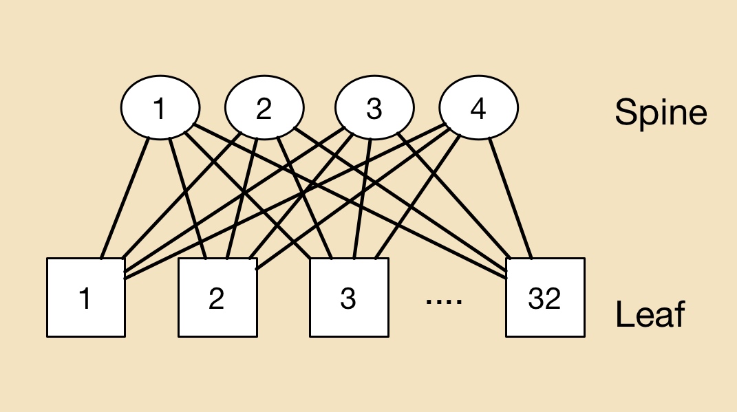 A leaf-spine architecture
The leaf and spine switches are built using ASICs, with the largest ICs typically having 32, 100 gigabit ports. One switch ASIC may be used in a platform but as Rickman points out, larger switches may implement multiple stages such as a three-stage Clos architecture. As a result, traffic between servers on different leaves, travelling up and down the leaf-spine, may pass through five stages or hops but possibly as many as nine.
There is no replacement performance in this area
It is the switch IC’s capacity and port count that dictates the overall size of the leaf-spine network and therefore the number of servers that can be connected. Rockley’s goal is to develop a bigger switch building block making use of silicon photonics.
“The fundamental thing to address is making bigger switching elements,” says Rickman. “That way you can keep the number of stages in the network the same but still make bigger and bigger networks.” Rockley expects its larger building-block switch will reduce the switch stages needed.
The UK start-up is not yet detailing its switch beyond saying it uses optical switching and that the company is developing a photonic integrated circuit (PIC) and a controlling ASIC.
“In the field of silicon photonics, for the same area of silicon, you can produce a larger switch; you have more capacity than you do in electronics,” says Rickman. Moreover, Rockley says that its silicon photonics-based PIC will scale with Moore’s law, with its switch's data capacity approximately doubling every two years. “Previously, the network did not scale with Moore’s law,” says Rickman.
Customers can see something is real and that it works. We are optimising all the elements of the system before taping out the fully integrated devices
Status
The company has developed a switch prototype that includes ‘silicon photonics elements’ and FPGAs. “Customers can see something is real and that it works,” says Rickman. “We are optimising all the elements of the system before taping out the fully integrated devices.” Rockley expects to have its switch in volume production in 2017.
Last year the company raised its first round of funding and said that it would undergo a further round in 2015. Rockley has not said how much it has raised or the status of the latest round. “We are well-funded and we have a very supportive group of investors,” says Rickman.
Rickman has long been involved in silicon photonics, starting out as a researcher at the University of Surrey developing silicon photonics waveguides in the early 1990s, before founding Bookham Technologies (now Oclaro). He has also been chairman of silicon photonics start-up Kotura that was acquired by Mellanox Technologies in 2013. Rickman co-founded Rockley in 2013.
“What I’ve learned about silicon photonics, and about all those electronics technologies, is how to design stuff from a process point of view to make something highly manufacturable and at the same time having the performance,” says Rickman.
There is no replacement performance in the area of data centre switching, he stresses: “The benefit of our technology is to deliver the performance, not the fact that it is cheap or [offers] average performance.”
For Part 2, Interconnection networks - an introduction, click here
Silicon photonics economics set to benefit III-V photonics
Silicon photonics promises to deliver cheaper optical components using equipment, processes and fabrication plants paid for by the chip industry. Now, it turns out, traditional optical component players using indium phosphide and gallium arsenide can benefit from similar economies, thanks to the wireless IC chip industry.
 Valery TolstikhinSilicon photonics did a good thing; it turned the interest of the photonics industry to the operational ways of silicon
So argues Valery Tolstikhin, head of a design consultancy, Intengent, and former founder and CTO of Canadian start-up OneChip Photonics. The expectations for silicon photonics may yet to be fulfilled, says Tolstikhin, but what the technology has done is spark interest in the economics of component making. And when it comes to chip economics, volumes count.
“For III-V photonics - indium phosphide and related materials - you have all kinds of solutions, designs and processes, but all are boutique,” says Tolstikhin. “They are not commercialised in a proper way and there is no industrial scale.” The reason for this is simple: optical components is a low-volume industry.
This is what Tolstikhin seeks to address by piggybacking on high-volume indium phosphide and gallium arsenide fabrication plants that make monolithic microwave integrated circuits (MMICs) for wireless.
“To take photonics out of boutique fabs, you need to do some standardisation and move to a fabless model, then you can load the fabs day and night with wafers,” says Tolstikhin. “That is the only way to make a process mature, reproducible and reliable.”
Tolstikhin has spent the last decade pursuing this approach. “The idea is to use something available in indium phosphide which is relatively close to a pure-play foundry.” A pure-play foundry is a fab that makes chips but does not design, market or sell them as its own products.
Tolstikhin’s first involvement was at start-up OneChip Photonics which developed an indium-phosphide platform that used a variety of photonic devices to make photonic integrated circuits (PICs), based on a commercial MMIC process.
The issue with III-V integrated photonics is that to implement different functions - a passive waveguide and a laser, for example - different materials are needed. “What makes a low-loss passive waveguide, does not work for the laser,” says Tolstikhin.
To overcome this, the wafer is repeatedly etched in certain areas, to remove unwanted material, and new layers grown instead with the required material, a process known as selective-area etch and regrowth. This is a complicated and relatively low-yield process that is custom to companies and their fabs, he says: “This is how all commercial lasers and PICs are made.”
In contrast, MMICs using indium phosphide do not need regrowth, simplifying the process considerably. To use a MMIC fab for an optical design, however, it must be developed in a way that avoids the need for regrowth stages.
“At OneChip we believe we did the first commercial laser - not just the laser but the PIC with it - regrowth-free,” says Tolstikhin. “It was made in a MMIC fab, that is the key.”
“To take photonics out of boutique fabs, you need to do some standardisation and move to a fabless model, then you can load the fabs day and night with wafers”
Wafer economics
To understand the relative economics, Tolstikhin compares the number of wafers - wafer starts - processed in silicon, indium phosphide and gallium arsenide.
One large TSMC fab has 400,000 12-inch CMOS wafer starts a year whereas globally the figure is equivalent to some 70 million such wafers a year. For MMICs, one fab Tolstikhin works with has 15,000 4-inch indium phosphide wafer starts a year whereas a large optical component company uses just a couple of thousand 3-inch indium phosphide wafers a year.
“In photonics, the [global] volumes – even for components going into the most massive markets like PON and the data centre interconnects – are still very low,” says Tolstikhin.
Gallium arsenide is somewhere in between: Win’s fab in Taiwan, which makes power amplifiers for wireless and other MMICs, has 250,000 6-inch wafers starts a year, while TriQuint’s fab in USA, with similar product line in wireless, totals 150,000 6-inch wafer starts a year.
Such volumes are not negligible and exceed all the needs of photonics, he says, enabling photonics to make claims similar to those trumpeted for silicon photonics: a mature process with a well-established quality system and, with its volumes, delivers better economics.
Moreover, if applications that currently are based on indium phosphide could be transferred to gallium arsenide, that would give an order of magnitude economies of scale, says Tolstikhin: “One example is mid-reach single-mode optical interconnects with an operating wavelength around 1060 nm, with gallium arsenide used for the transmitter, receiver and transceiver PICs”.
And while the scale of III-V semiconductor manufacturing may still be much lower than CMOS, the up-front cost involved in using a III-V fab is also much less.
Using III-V semiconductors for analogue electronics like the laser /modulator drivers or the trans-impedance amplifier also delivers a speed advantage: heterojunction bipolar transistors (HBTs) in indium phosphide have been demonstrated working at up to 400 GHz, and these, being vertical devices, do not have their speed scaled with lithography. In contrast, CMOS analog electronics is much slower and its device speed is scalable with lithography resolution. A 130 nm CMOS process, the starting point for silicon photonics, cannot support optical components with bit rates beyond 10 Gbps.
Design house
Intengent, Tolstikhin’s company, acts as a bridge between OEMs building optical components and sub-systems and the III-V foundries making photonic chips for them.
He compares Intengent to what application-specific IC (ASIC) companies used to do for the electronic chip industry. Intengent works with the OEM to specify and design the photonic chip based on its system application and then works with the fab to develop and turn the chip into a product by meeting its design rules and process capabilities.
“The aim is that you can go and design within existing fabs and processes something that meets the customer’s application and requirements,” he says.
Tolstikhin is also working with ELPHiC, a Canadian start-up that is raising funding to develop single-mode mid-board optics. The indium-phosphide design combines analogue electronic circuitry with the photonics.
“It appears the best way [to do mid-board optics] is based on electronic and photonic integration onto one substrate and indium phosphide is a natural choice for such a substrate,” he says.
Tolstikhin makes clear he is not against silicon photonics. “It did a good thing; it turned the interest of the photonics industry to the operational ways of silicon: standardised processes, pure-play foundries, device designs separate from the semiconductor physics, and circuit designs separate from the wafer processing.”
As a result, something similar is now being pursued in III-V photonics.
IBM demos a 100 Gigabit silicon photonics transceiver
“It is a demonstration vehicle illustrating the complex design capabilities of the technology and the functionality of the optical and electrical components,” says Will Green, manager of IBM’s silicon integrated nano-photonics group.
 Will Green
IBM has been developing silicon photonics technology for over a decade, starting with building-block optical functions based on silicon, to its current monolithic system-on-chip technology that includes design tools, testing and packaging technologies.
Now this technology is nearing commercialisation.
“We do plan to have the technology available for use within IBM’s systems but also within the larger market; large-volume applications such as the data centre and hyper-scale data centres in particular,” says Green.
IBM is already working with companies developing their own optical component designs using its technology and design tools. “These are tools that circuit designers are familiar with, such that they do not need to have an in-depth knowledge of photonics in order to build, for example, an optical transceiver,” says Green.
We do plan to have the technology available for use within IBM’s systems but also within the larger market
100 gig demonstrator
IBM refers to its silicon photonics technology as CMOS-integrated nano-photonics. CMOS-integrated refers to the technology’s monolithic nature that combines CMOS electronics with photonics on one substrate. Nano-photonics highlights the dimensions of the feature sizes used.
IBM is rare among the silicon photonics community in combining electronics and photonics on one chip; other players implement photonics and electronics on separate dies before combining the two. What is not included is the laser which is externally attached using fibre.
The platform supports 25 gigabit speeds as well as wavelength division multiplexing. Originally, IBM started with 90 nm CMOS using bulk silicon before transferring to a silicon-on-insulator (SOI) substrate. An SOI wafer is ideal for creating optical waveguides that confine light using the large refractive index difference between silicon and silicon dioxide. However, to make the electrical devices run at 25 gigabit, the resulting transistor gate length ended up being closer to a 65 nm CMOS process.
 Source: IBM Corporation.
IBM's optical waveguides are sub-micron, having dimensions of a few hundred nanometers. This is the middle ground, says Green, trading off the density of smaller-dimensioned waveguides with larger, micron-plus ones that deliver low propagation loss.
Also used are sub-wavelength optical 'metamaterial' structures that transition between the refractive index of the fibre and that of the optical waveguide to achieve a good match between the two. “These very tiny sub-wavelength structures are made using lithography near the limits of what is available,” says Green. “We are engineering the optical properties of the waveguide in order to achieve a low insertion loss when bringing the fibre onto the chip.” The single mode fibre to the chip is attached using passive alignment.
The 100 gigabit transceiver demonstrator uses four 25 gigabit coarse wavelengths around 1310 nm. The technology is suited to implement the CWDM4 MSA.
The whole technology is available to be commercialised by any chip manufacturer
“We are working with four wavelengths today but in the same way as telecom uses many wavelengths, we can follow a similar path,” says Green.
The chip design features transmitter electronics - a series of amplifiers that boost the voltage to drive the Mach-Zehnder Interferometer modulators - and a multiplexer to combine the four wavelengths onto the fibre while the receiver circuitry includes a demultiplexer, four photo-detectors and trans-impedance amplifiers and limiting amplifiers, says Green. What is lacking to make the 100 gigabit transceiver functional is a micro-controller, feedback loops to control the temperature of key circuits, and the circuitry to interface to standard electrical input/ output.
Green highlights how the bill of materials of a chip is only a fraction of the total cost since assembly and testing must also be included.
“We reduce the cost of assembly through automated passive optical alignment and the introduction of custom structures onto the wafer,” he says. “We believe we can make an impact on the cost structure of the optical transceiver and where this technology needs to be to access the data centre.” IBM has also developed a way to test the transceiver chips at the wafer level.
Green admits that its CMOS-integrated nanophotonics process will not scale beyond 25 gigabit as the 90-65 nm CMOS is not able to implement faster serial rates. But IBM has already shown an optical implementation of the PAM-4 modulation scheme that doubles a link's rate to 50 gigabit.
Meanwhile, IBM’s process design kit (PDK) is already with customers. A PDK includes documents and data files that describe the fabrication process and enable a user to complete a design. A PDK includes a fab’s process parameters, mask layout instructions, and the library of silicon photonics components; grating couplers, waveguides, modulators and the like [1].
“They [customers] have used the design kit provided by IBM but have built their own designs,” says Green. “And now they are testing hardware.”
IBM is keen that its silicon photonics technology will be licensed and used by circuit design houses. "Houses that bring their own IP [intellectual property], use the enablement tools and manufacture at a site that is licensing the technology from IBM,” says Green. "The whole technology is available to be commercialised by any chip manufacturer.”
Reference
[1] Silicon Photonics Design: From Devices to Systems, Lukas Chrostowski and Michael Hochberg, Cambridge University Press, 2015. Click here
Altera’s 30 billion transistor FPGA
- The Stratix 10 features a routing architecture that doubles overall clock speed and core performance
- The programmable family supports the co-packaging of transceiver chips to enable custom FPGAs
- The Stratix 10 family supports up to 5.5 million logic elements
- Enhanced security features stop designs from being copied or tampered with
Altera has detailed its most powerful FPGA family to date. Two variants of the Stratix 10 family have been announced: 10 FPGAs and 10 system-on-chip (SoC) devices that include a quad-core 64-bit architecture Cortex-A53 ARM processor alongside the programmable logic. The ARM processor can be clocked at up to 1.5 GHz.
The Stratix 10 family is implemented using Intel’s 14nm FinFET process and supports up to 5.5 million logic elements. The largest device in Altera’s 20nm Arria family of FPGAs has 1.15 million logic elements, equating to 6.4 billion transistors. “Extrapolating, this gives a figure of some 30 billion transistors for the Stratix 10,” says Craig Davis, senior product marketing manager at Altera.
 Altera's HyperFlex routing architecture. Shown (pointed to by the blue arrow) are the HyperFlex registers that sit at the junction of the interconnect traces. Also shown are the adaptive logic module blocks. Source: Altera.
The FPGA family uses a routing fabric, dubbed HyperFlex, to connect the logic blocks. HyperFlex is claimed to double the clock speed compared to designs implemented using Altera’s Stratix V devices, to achieve gigahertz rates. “Having that high level of performance allows us to get to 400 gigabit and one terabit OTN (Optical Transport Network) systems,” says Davies.
The FPGA company detailed the Stratix 10 a week after Intel announced its intention to acquire Altera for US $16.7 billion.
Altera is also introducing with the FPGA family what it refers to as heterogeneous 3D system packaging and integration. The technology enables a designer to customise the FPGA’s transceivers by co-packaging separate transceiver integrated circuits (ICs) alongside the FPGA.
Different line-rate transceivers can be supported to meet a design's requirements: 10, 28 or 56 gigabit-per-second (Gbps), for example. It also allows different protocols such as PCI Express (PCIe), and different modulation formats including optical interfaces. Altera has already demonstrated a prototype FPGA co-packaged with optical interfaces, while Intel is developing silicon photonics technology.
HyperFlex routing
The maximum speed an FPGA design can be clocked is determined by the speed of its logic and the time it takes to move data from one part of the chip to another. Increasingly, it is the routing fabric rather than the logic itself that dictates the total delay, says Davis.
This has led the designers of the Stratix 10 to develop the HyperFlex architecture that adds a register at each junction of the lines interconnecting the logic elements.
Altera first tackled routing delay a decade ago by redesigning the FPGA’s logic building block. Altera went from a 4-input look-up table logic building block to a more powerful 8-input one that includes output registers. Using the more complex logic element - the adaptive logic module (ALM) - simplifies the overall routing. “You are essentially removing one layer of routing from your system,” says Davies.
When an FPGA is programmed, the file is presented that dictates how the wires and hence the device’s logic are connected. The refinement with HyperFlex is that there are now registers at those locations where the switching between the traces occurs. A register can either be bypassed or used.
“It allows us to put the registers anywhere in the design, essentially placing them in an optimum place for a given route across the FPGA,” says Davies. The number of hyper-registers in the device's routing outnumber the standard registers in the ALM blocks by a factor of ten.
Using the registers, designers can introduce data pipelining to reduce overall delay and it is this pipelining, combined with the advanced 14nm CMOS process, that allows a design to run at gigahertz rates.
“We have made the registers small but they add one or two percent to the total die area, but in return it gives us the ability to go to twice the performance,” says Davies. “That is a good trade-off.
The biggest change getting HyperFlex to work has been with the software tools, says Davies. HyperFlex and the associated tools has taken over three years to develop.
“This is a fundamental change,” says Davies. “It [HyperFlex] is relatively simple but it is key; and it is this that allows customers to get to this doubling of core performance.”
The examples cited by Altera certainly suggest significant improvements in speed, density, power dissipation, but I want to see that in real-world designs
Loring Wirbel, The Linley Group
Applications
Altera says that over 100 customer designs have now been processed using the Stratix 10 development tools.
It cites as an example a current 400 gigabit design implemented using a Stratix V FPGA that requires a bus 1024-bits wide, clocked at 390MHz. The wide bus consumes considerable chip area and routing it to avoid congestion is non-trivial.
Porting the design to a Stratix 10 enables the bus to be clocked at 781MHz such that the bus width can be halved to 512 bits. “It reduces congestion, makes it easier to do timing closure and ship the design,” says Davies. “This is why we think Stratix 10 is so important for high-performance applications like OTN and data centres.” Timing closure refers to the tricky part of a design where the engineer may have to iterate to ensure that a design meets all the timing requirements.
For another, data centre design, a Stratix 10 device can replace five Stratix V ICs on one card. The five FPGAs are clocked at 250MHz, run PCIe Gen2 x8 interfaces and DDR3 x72 memory clocked at 800MHz. Overall the power consumed is 120W. Using one Stratix 10 chip clocked at 500MHz, faster PCIe Gen3 x8 can be supported as can a wider DDR3 x144 memory clocked at 1.2GHz, with only 44W consumed.
Loring Wirbel, senior analyst at The Linley Group, says that Altera’s insertion of pipelined registers to cut average trace lengths is unique.
“The more important question is, can the hyper-register topology regularly gain the type of advantages claimed?” says Wirbel. “The examples cited by Altera certainly suggest significant improvements in speed, density, power dissipation, but I want to see that in real-world designs.”
We are also looking at optical transceivers directly connected to the FPGA
Craig Davies, Altera
Connectivity tiles
Altera recognises that future FPGAs will support a variety of transceiver types. Not only are there different line speeds to be supported but also different modulation schemes. “You can’t build one transceiver that fits all of these requirements and even if you could, it would not be an optimised design,” says Davies.
Instead, Altera is exploiting Intel’s embedded multi-die interconnect bridge (EMIB) technology to interface the FPGA and transceivers, dubbed connectivity tiles. The bridge technology is embedded into the chip’s substrate and enables dense interconnect between the core FPGA and the transceiver IC.
Intel claims fewer wafer processing steps are required to make the EMIB compared to other 2.5D interposer processes. An interposer is an electrical design that provides connectivity. “This is a very simple ball-grid sort of interposer, nothing like the Xilinx interposer,” says Wirbel. “But it is lower cost and not intended for the wide range of applications that more advanced interposers use.”
Using this approach, a customer can add to their design the desired interface, including optical interfaces as well as electrical ones. “We are also looking at optical transceivers directly connected to the FPGA,” says Davies.
Wirbel says such links would simplify interfacing to OTN mappers, and data centre designs that use optical links between racks and for the top-of-rack switch.
“Intel wants to see a lot more use of optics directly on the server CPU board, something that the COBO Alliance agrees with in part, and they may steer the on-chip TOSA/ ROSA (transmitter and receiver optical sub-assembly) toward intra-board applications,” he says.
But this is more into the future. “It's fine if Intel wants to pursue those things, but it should not neglect common MSAs for OTN and Ethernet applications of a more traditional sort,” says Wirbel.
The benefit of the system-in-package integration is that different FPGAs can be built without having to create a new expensive mask set each time. “You can build a modular lego-block FPGA and all that it has different is the packaged substrate,” says Davies.
Security and software
Stratix 10 also features security features to protect companies’ intellectual property from being copied or manipulated.
The FPGA features security hardware that protects circuitry from being tampered with; the bitstream that is loaded to configure the FPGA must be decrypted first.
The FPGA is also split into sectors such that parts of the device can have different degrees of security. The sectoring is useful for cloud-computing applications where the FPGA is used as an accelerator to the server host processor. As a result, different customers’ applications can be run in separate sectors of the FPGA to ensure that they are protected from each other.
The security hardware also allows features to be included in a design that the customer can unlock and pay for once needed. For example, a telecom platform could be upgraded to 100 Gigabit while the existing 40 Gig live network traffic runs unaffected in a separate sector.
Altera has upgraded its FPGA software tools in anticipation of the Stratix 10. Features include a hierarchical design flow to simplify the partitioning of a design project across a team of engineers, and the ability to use cloud computing to speed up design compilation time.
What applications will require such advanced FPGAs, and which customers will be willing to pay a premium price for? Wirbel says the top applications will remain communications.
“The emergence of new 400 Gig OTN transport platforms, and the emergence of all kinds of new routers and switches with 400 Gig interfaces, will keep a 40 percent communication base for FPGAs overall solid at Altera,” he says.
Wirbel also expects server accelerator boards where FPGA-based accelerators are used for such applications as financial trading and physics simulation will also be an important market. “But Intel must consider the accelerator board market as an ideal place for Stratix 10 on its own, and not merely as a vehicle for promoting a future Xeon-plus-FPGA hybrid,” he says.
Altera will have engineering samples of the Stratix 10 towards the end of 2015, before being shipped to customers.
Moore's law and silicon photonics
Chip pioneer Gordon E. Moore’s article appeared in the magazine Electronics in 1965. Dr. Moore was the director of the R&D labs at Fairchild Semiconductor, an early maker of transistors. Moore went on to co-found Intel, then a memory company, becoming its second CEO after Robert Noyce.
Moore’s article was written in the early days of integrated circuits. At the time, silicon wafers were one inch in diameter and integrating 50 components on a chip was deemed a state-of-the-art design.
Moore observed that, at any given time, there was an ideal number of components that achieved a minimum cost. Add a few more components and the balance would be tipped: the design would become overly complex, wafer yields would go down and costs would rise.
His key insight, later to become known as Moore’s law, was that integrated circuit complexity at this minimum cost was growing over time. Moore expected the complexity to double each year for at least another decade.
In his article he predicted that, by 1970, the manufacturing cost per component would be a tenth of the cost in 1965. Extrapolating the trend further, Moore believed that “by 1975, the number of components per integrated circuit for minimum cost will be 65,000 components.” Moore was overly optimistic, but only just: in 1975, Intel was developing a chip with 32,000 transistors.
“Perhaps we can say that the future of silicon photonics is the future of electronics itself.”
One decade after his article, Moore amended his law to a doubling of complexity every 24 months. By then the industry had started talking about transistors rather than components - circuit elements such as transistors, resistors and capacitors - after alighting on complementary metal oxide semiconductor (CMOS) technology to make the bulk of its chips. And in the years that followed, the period of complexity-doubling settled at every 18 months.
Moore has received less credit for his article's remarkable foresight regarding the importance of integrated circuits, especially when, in 1965, their merits were far from obvious. Such devices would bring a proliferation of electronics, he said, “pushing this science into many new areas”.
He foresaw home computers “or at least terminals connected to a central computer’, automatic control for automobiles and even mobile phones - ‘personal portable communications equipment’ as he called them. The biggest potential of ICs, he said, would be in the making of systems, with Moore highlighting computing, and telephone communications and switches.
The shrinking transistor
The shrinking of the transistor has continued ever since. And the technological and economic consequences have been extraordinary.
As a recent 50th anniversary Moore’s law article in IEEE Spectrum explains (link above), the cost of making a transistor in 1965 was $30 at today’s costs, in 2015 it is one billionth of a dollar. And in 2014, the semiconductor industry made 250 billion billion transistors, more transistors than had been made in all the years of the semiconductor industry up to 2011.
But the shrinking of the transistor cannot continue indefinitely, especially as certain transistor dimensions approach the atomic scale. As a result, many of the benefits that resulted with each shift to a new, smaller feature-sized CMOS process no longer hold.
To understand why, some understanding of CMOS and in particular, the MOS field effect transistor (MOSFET), is required.
Current flow between a MOSFET’s two terminals - the source and the drain - is controlled by a voltage placed on a third, electrical contact known as a gate. The gate comprises a thin layer of metal oxide, an oxide insulator on which sits a metal contact.
Several key dimensions define the MOSFET including the thickness of the oxide, the width of the source and the drain, and the gate length - the distance between the source and the drain.
Dennard scaling, named after IBM engineer and inventor of the DRAM, Robert Dennard, explains how the key dimensions of the transistor can all shrunk by the same factor, generation after generation. It is the effect of this scaling that makes Moore’s law work.
From the 1970s to the early 2000s, shrinking the transistor’s key dimension by a fixed factor returned a guaranteed bounty. More transistors could be placed on a chip allowing more on-chip integration, while each transistor became cheaper.
In turn, for a given chip area, the chip’s power density - the power consumption over a given area - remained constant. There may be more transistors crammed into a fixed area but the power each one consumes is less.
The predictable era of scaling transistors, after 50 years, is coming to an end and the industry is set to change
The transistor gate length feature size is used to define the CMOS technology or process node. In 1980, the minimum feature size was around 3 microns, nowadays CMOS chips typically use a 28 nanometer feature size - a 100 fold reduction. The metal oxide thickness has also been reduced one hundred times over the years.
But in the last decade Dennard scaling has come to an end.
The gate’s oxide thickness can no longer be trimmed as its dimensions are only a few atoms thick. The voltage threshold, the voltage applied to the gate to turn the transistor on, has also stopped shrinking, which in turn has stopped the scaling of the transistor’s upper voltage.
Why is this important? Because no longer being able to scale all these key parameters has meant that while smaller transistors can still be made, their switching speed is no longer increasing, nor is the power density constant.
Moreover, the very success of the relentless scaling means that the transistors are so tiny that new effects have come into play.
Transistors now leak current even when they are in the ‘off’ state. This means they consume power not only when they are being switched at high speed - the active power - but also they consume leakage power when they are off due to this current.
Process engineers now must work harder, to develop novel transistor designs and new materials to limit the leakage current. A second issue associated with the prolonged success of Dennard scaling is variability. Transistors are now less reliable and their performance less predictable.
The end of Dennard scaling means that the chip companies’ motivation to keep shrinking transistors is more to do with device cost rather than performance.
If, before, the power density stayed fixed with each new generation of CMOS process, more recently it has been the cost of manufacturing of a given area of silicon that has stayed fixed.
As the IEEE Spectrum Moore’s law article explains, this has been achieved by a lot of engineering ingenuity and investment. Device yield has gone up from 20 percent in the 1970s to between 80 and 90 percent today. The size of the silicon wafers on which the chips are made has also increased, from 8 inches to 12 inches. And while the lithography tools now cost one hundred-fold more than 35 years ago, they also pattern the large wafers one hundred times faster.
But now even the cost of making a transistor has stopped declining, according to The Linley Group, with the transition point being around the 28nm and 20nm CMOS.
Silicon manufacturing innovation will continue, and transistors will continue to shrink. Leading chip companies have 14nm CMOS while research work is now at a 7nm CMOS process. But not everyone will make use of the very latest processes, given how these transistors will be more costly.
Beyond Moore’s law
The industry continues to debate how many years Moore’s law still has. But whether Moore’s law has another 10 years or not, it largely does not matter.
Moore’s law has done its job and has brought the industry to a point where it can use billions of transistors for its chip designs.
But to keep expanding computing performance, new thinking will be required at many levels, spanning materials, components, circuit design, architectures and systems design.
The predictable era of scaling transistors, after 50 years, is coming to an end and the industry is set to change.
IBM announced last year its plan to invest US $3 billion over five years to extend chip development. Areas it is exploring include quantum computing, neurosynaptic computing, III-V technologies, carbon nanotubes, graphene, next-generation low-power transistors, and silicon photonics.
Silicon photonics
The mention of silicon photonics returns us to Gordon Moore’s 1965 article. The article starts with a bang: “The future of integrated electronics is the future of electronics itself".
Can the same be said of photonics?
Is the future of integrated photonics the future of photonics itself?
Daryl Inniss, vice president of Ovum’s components practice, argues this is certainly true. Photonics may not have one optical building block like electronics has the transistor, nor is there any equivalent of Dennard scaling whereby shrinking photonic functions delivers continual performance benefits.
But photonic integration does bring cost benefits, and developments in optical interconnect and long-haul transmission are requiring increasing degrees of integration, the sort of level of component integration associated with the chip industry at the time of Moore’s article.
And does the following statement hold true? “The future of silicon photonics is the future of photonics itself.”
“I think silicon photonics is bigger than photonics itself,” says Inniss. “Where do you draw the line between photonics and electronics? IBM, Intel and STMicroelectronics are all suppliers of electronics.”
Inniss argues that silicon photonics is an electronics technology. “Perhaps we can say that the future of silicon photonics is the future of electronics itself.”
Graphene prototype modulator shown working at 10 Gigabit
- Imec's graphene electro-absorption modulator works at 10 Gigabit-per-second
- The modulator is small and has be shown to be thermally stable
- Much work is required to develop the modulator commercially
 Cross-section of the graphene electro-absorption modulator. The imec work was first detailed in a paper at the IEDM conference held in December 2014 in San Francisco. Source: imec
Imec has demonstrated an optical modulator using graphene operating at up to 10 Gigabit. The Belgium nano-electronics centre is exploring graphene - carbon atoms linked in a 2D sheet - as part of its silicon photonics research programme investigating next-generation optical interconnect. Chinese vendor Huawei joined imec's research programme late last year.
Several characteristics are sought for a modulator design. One is tiny dimensions to cram multiple interfaces in as tight a space as possible, as required for emerging board-to-board and chip-to-chip optical designs. Other desirable modulator characteristics include low power consumption, athermal operation, the ability to operate over a wide range of wavelengths, high speed (up to 50 Gbps) and ease of manufacture.
Imec's interest in graphene stems from the material's ability to change its light-absorbing characteristics over a wide spectral range. "Graphene has a high potential for a wide-band modulator solution and also for an athermal design," says Joris Van Campenhout, programme director for optical I/O at imec.
 Source: Gazettabyte
Modulation
For optical modulation, either a material's absorption coefficient or its refractive index is used. Silicon photonics has already been used to implement Mach-Zehnder interferometer and ring resonator modulators. These designs modifying their refractive index and use interference to induce light intensity modulation.
"Mach-Zehnder modulators have been optimised dramatically over the last decade," says Van Campenhout. "They can generate at very high bit rates but they are still pretty big - 1mm or longer - and that prevents further scaling."
Ring resonators are more compact and have been shown working at up to 50 Gigabit. "But they are resonant devices; they are wavelength-specific and thermally dependent," says Van Campenhout. "A one degree change can detune the ring resonance from the laser's wavelength."
The other approach, an electro-absorption modulator, uses an electric field to vary the absorption coefficient of the material and this is the graphene modulator approach imec has chosen.
Electro-absorption modulators using silicon germanium meet the small footprint requirement, have a small capacitance and achieve broadband operation. Capacitance is an important metric as it defines the modulator's maximum data rate as well as such parameters as insertion loss (how many dBs of signal are lost passing through the modulator) and the extinction ratio (a measure of the modulator's on and off intensity).
"Silicon germanium offers a pretty decent modulation quality," says Van Campenhout but the wavelength drifts with temperature. Thermal drift is something that graphene appears to solve.
Imec's graphene electro-absorption modulator comprises a 50 micron graphene-oxide-silicon capacitor structure residing above a silicon-on-insulator rib waveguide. The waveguides are implemented using a 200mm wafer whereas the graphene is grown on a copper substrate before being placed on the silicon die. Van Campenhout refers to the design as hybrid or heterogenous silicon photonics.
The graphene modulator exhibits a low 4dB insertion loss and an extinction ratio of 2.5dB. The device's performance is stable over a broad spectrum: an 80nm window centred around the 1550nm wavelength. The performance of up to 10Gbps was achieved over a temperature range of 20-49°C.
"The key achievement is that we have been able to show that you can operate at 10 Gigabit with very clean modulation eye diagrams," says Van Campenhout. However, much work is needed before the device becomes a viable technology.
 Source: Gazettabyte, imec
What next?
Imec has modelled the graphene modulator using a simple resistor-capacitor circuit. "We have been able to identify sources of capacitance and resistance," says Van Campenhout. "We can now better optimise the design for speed or for efficiency."
The speed of the modulator is dictated by the resistance-capacitance product. Yet the higher the capacitance, the greater the efficiency: the better the extinction ratio and the lower the insertion loss. "So it comes down to reducing the resistance," says Van Campenhout. "We think we should be able to get to 25 Gigabit."
With the first prototype, the absorption effect induced by the electric field is achieved between a single graphene plate and the silicon. Imec plans to develop a design using two graphene plates. "If two slabs of graphene are used, we expect to double the effect," says Van Campenhout. "All the charge on both plates of the capacitor will contribute to the modulation of the absorption."
However the integration is more difficult with two plates, and two metal contacts to graphene are needed. "This is still a challenge to do," says Van Campenhout.
Imec has also joined the Graphene Flagship, the European €1 billion programme that spans materials production, components and systems. "One of the work packages is to show you can process on a manufacturing scale graphene-based devices in a CMOS pilot line," he says. Another consideration is to use silicon nitride waveguides rather than silicon ones as these can be more easily deposited.
One challenge still to be overcome is the development of an efficient graphene-based photo-detector. "If this technology is ever going to be used in a real application, there should be a much more efficient graphene photo-detector being developed," says Van Campenhout.