
Marvell exploits 5nm CMOS to add Octeon 10 DPU smarts

The Octeon family has come a long way since the networking infrastructure chip was introduced by Cavium Networks in 2005.
Used for data centre switches and routers, the original chip family featured 1 to 16, 64-bit MIPS cores and hardware acceleration units for packet processing and encryption. The devices were implemented using foundry TSMC’s 130nm CMOS process.
Marvell, which acquired Cavium in 2018, has taped out the first two devices of its latest, seventh-generation Octeon 10 family.
The devices, coined data processing units (DPU), will feature up to 36 state-of-the-art ARM cores, support a 400-gigabit line rate, 1 terabit of switching capacity, and dedicated hardware for machine-learning and vector packet processing (VPP).
Marvell is using TSMC’s latest 5nm CMOS process to cram all these functions on the DPU system-on-chip.
The 5nm-implemented Octeon 10 coupled with the latest ARM cores and improved interconnect fabric will triple data processing performance while halving power consumption compared to the existing Octeon TX2 DPU.
DPUs join CPUs and GPUs
The DPU is not a new class of device but the term has become commonplace for a processor adept at computing and moving and processing packets.
Indeed, the DPU is being promoted as a core device in the data centre alongside central processing units (CPUs) and graphic processing units (GPUs).
As Marvell explains, a general-purpose CPU can perform any processing task but it doesn’t have the computational resources to meet all requirements. For certain computationally-intensive tasks like graphics and artificial intelligence, for example, the GPU is far more efficient.
The same applies to packet processing. The CPU can perform data-plane processing tasks but it is inefficient when it comes to intensive packet processing, giving rise to the DPU.
“The CPU is just not effective from a total cost of ownership, power and performance point of view,” says Nigel Alvares, vice president of solutions marketing at Marvell.
Data-centric tasks
The DPU is used for smart network interface controller (SmartNIC) cards found in computer servers. The DPU is also suited for standalone tasks at the network edge and for 5G.
Marvell says the Octeon DPU can be used for data centres, 5G wireless transport, SD-WAN, and fanless boxes for the network edge.
Data centre computation is moving from application-centric to more data-centric tasks, says Marvell. Server applications used to host all the data they needed when executing algorithms. Now applications gather data from various compute clusters and locations.
“The application doesn’t have all the data but there is a lot of data that needs to be pumped into the application from many points,” says Jeffrey Ho, senior product manager at Marvell. “So a lot of network overlay, a lot of East-West traffic.”
This explains the data-centric nature of tasks or, as Ho describes it, the data centre appearing as a mesh of networks: “It’s a core network, it is a router network, it is an enterprise network – all in one block.”
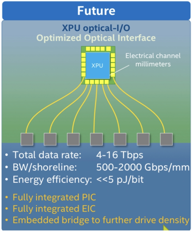
Octeon 10 archtecture
The Octeon 10 family uses ARM’s latest core architecture, the Neoverse N2 processor, Arm’s first Armv9 Infrastructure CPU, for general-purpose computational tasks. Each ARM core has access to hierarchical cache memory and external DDR5 SDRAM memory.
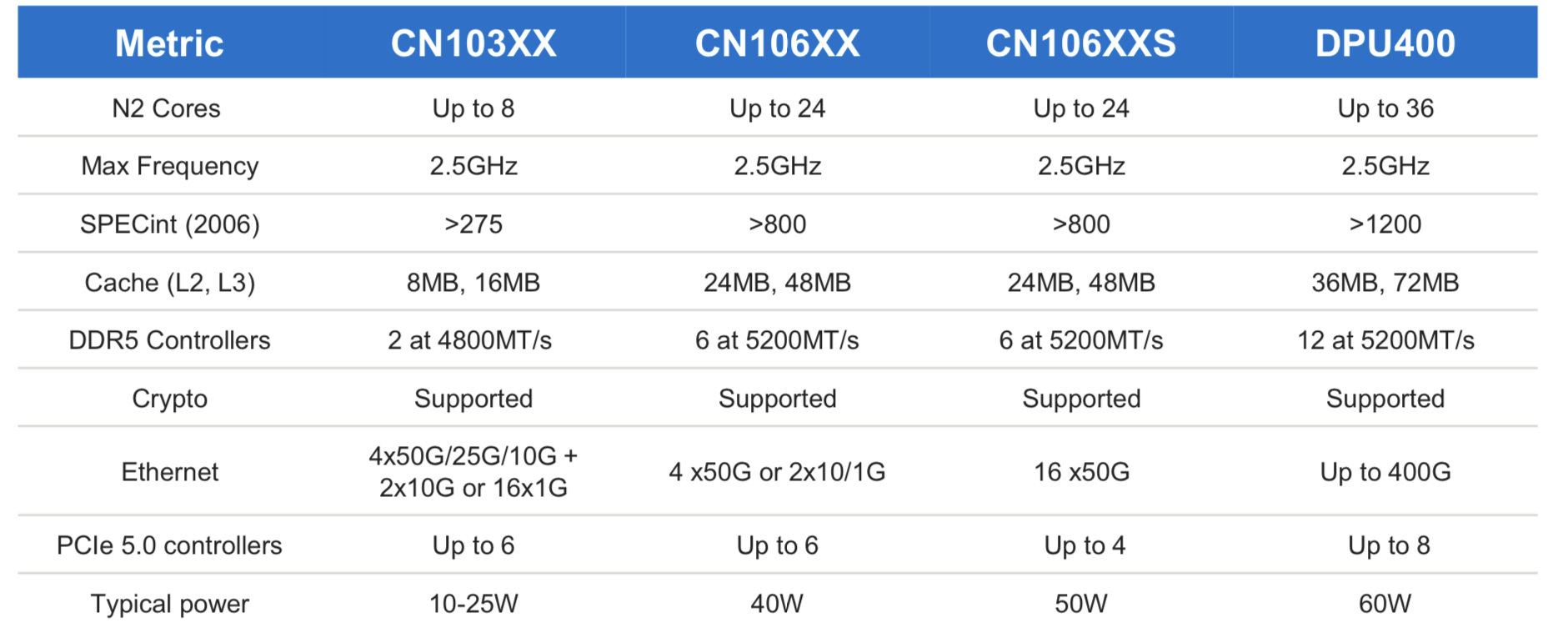
The initial Octeon 10 family members range from the CN103XX which has up to eight ARM N2 cores, each with Level 1 and private Level 2 cache and shared level 2 and 3 caches (8MB and 16MB, respectively).
The most powerful DPU of the Octeon 10 family is the DPU400 which will have up to 36 ARM cores and 36MB level 2 and 72MB level 3 caches.
“Then you have the acceleration hardware that is very friendly to this generic compute,” says Ho.
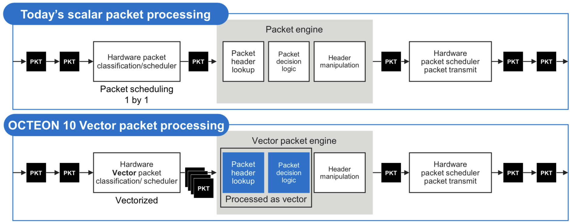
One custom IP block is for vector packet processing (VPP). VPP has become popular since becoming available as open-source software that batch-processes packets with similar attributes. Marvell says that until now, the hardware processed the packets one at a time such that the potential of VPP has not been fully realised.
The Octean 10 is the first device family to feature hardware for VPP acceleration. Accordingly, only one look-up table operation and one logical decision may be required before header manipulation is performed for each of the grouped packets. The specialised hardware accelerates VPP by between 3-5x.
The DPU also integrates on-chip hardware for machine-learning inferencing tasks.
Machine learning can be applied to traffic patterns on a compute cluster such that every day or so, newly learned models can be downloaded onto the DPU for smart malware detection. This is learnt behaviour; no rules need be written in code, says Marvell. Machine learning can determine if a packet is malware to an accuracy of 80 per cent, says Ho.
The hardware can even identify suspect packets by learning application types even when the packets themselves are encrypted using the IPSec protocol.
The DPU’s machine learning inference hardware can also be used for other tasks such as beamforming optimisation in cellular networks.
As for the 400-gigabit rating of the Octeon DPU, this is the maximum input and output that a CPU can cope with if every packet needs processing. And when each packet passes through the IPsec encyption engines, the maximum line rate is 400 gigabits.
In turn, if a packet need not pass through the CPU or no cryptography is required, one terabit of Layer 2/ Layer 3 switching can be done on-chip.
“All these are separate accelerator capability of the platform,” says Ho. The data path bandwidth of the DPU is 400Gbps+, IPSec throughput is 400Gbps+, and the switch capability is 1 terabit.”
Using software, the DPU accelerators are configured according to the data processing needs which may use all or some of the on-chip accelerators, he says.

4G and 5G cellular systems
For radio access networks, the radio head units talk to a distributed unit (DU) and a centralised unit (CU). (See diagram.)

The DU chassis houses six or eight line cards typically. The DU has a main controller that connects all the signals and backhauls them to the CU. This requires a two-chip solution with a switch chip next to each Octeon.
Using a 5nm process, the switch-integrated Octeon DPU reduces the DU’s overall power consumption and bill of materials. This Octeon DPU can be used for the DU, the fronthaul gateway and even the CU.
The DPU also exploits the 1-terabit switching capacity for the DU chassis example. Here, six Octeon Fusion-O chips, which perform Layer 1 processing, are connected to six radio units. Each of the six Fusion-O chips connects to the DPU via a 50-gigabit serialiser/ deserialiser (serdes).
Typical DU designs may use two Octeon DPUs, the second being a standby host DPU. This accounts for six line cards and two Octeon DPUs per DU chassis.
Market status
Marvell says that for 100-gigabit-throughput DPUs, up to 60 per cent of volumes shipped are used in the cloud and 40 per cent at the network edge.
Since throughput rates in the cloud are growing faster than the network edge, as reflected with the advent of 200- and 400-gigabit SmartNIC cards, the overall ratio of devices used for the cloud will rise.
The first two Octeon 10 devices taped out two months ago were the CN106XX and CN106XXS. These devices will sample in the second half of 2021.
The two will be followed by the CN103XX which is expected around spring 2022 and following that will be the DPU400.
Intel details its 800-gigabit DR8 optical module

The company earmarks 2023 for its first co-packaged optics product
Intel is sampling an 800-gigabit DR8 in an OSFP pluggable optical module, as announced at the recent OFC virtual conference and show.
“It is the first time we have done a pluggable module with 100-gigabit electrical serdes [serialisers/ deserialisers],” says Robert Blum, Intel’s senior director, marketing and new business. “The transition for the industry to 100-gigabit serdes is a big step.”
The 800-gigabit DR8 module has eight electrical 100-gigabit interfaces and eight single-mode 100-gigabit optical channels in each transmission direction.
Intel demonstrated a prototype 12.8-terabit co-packaged optics design
The attraction of the single-module DR8 design, says Blum, is that it effectively comprises two 400-gigabit DR4 modules. “The optical interface allows you the flexibility that you can break it out into 400-gigabit DR4,” says Blum. “You can also do single 100-gigabit breakouts or you can do 800-gigabit-to-800-gigabit traffic.”
Intel expects volume production of the DR8 in early 2022. Developing a DR8 in a QSFP-DD800 form factor will depend on customer demand, says Blum.
Intel will follow the 800-gigabit DR8 module with a dual 400G FR4, expected later in 2022. The company is also developing a 400-gigabit FR4 module that is expected then.
Meanwhile, Intel is ramping its 200-gigabit FR4 and 400-gigabit DR4 modules.
51.2-terabit co-packaged optics
Intel demonstrated a prototype 12.8-terabit co-packaged optics design, where the optics is integrated alongside its Tofino 2 Ethernet switch chip, at last year’s OFC event.
The company says its first co-packaged optics design will be for 51.2-terabit switches and is scheduled in late 2023. “We see smaller-scale deployments at 51.2 terabits,” says Blum.
Moving the industry from pluggable optical modules to co-packaged optics is a big shift, says Intel. The technology brings clear system benefits such as 30 per cent power savings and lower cost but these must be balanced against the established benefits of using pluggable modules and the need to create industry partnerships for the production of co-packaged optics.
The emergence of 800-gigabit client-side pluggable modules such as Intel’s also means a lesser urgency for co-packaged optics. “You have something that works even if it is more expensive,” says Blum.
Thirty-two 800-gigabit modules can serve a 25.6-terabit switch in a one rack unit (1RU) platform.
However, for Intel, the crossover point occurs once 102.4-terabit switch chips and 200-gigabit electrical interfaces emerge.
“We see co-packaged optics as ubiquitous; we think pluggables will no longer make sense at that point,” says Blum.
FPGA-based optical input-output
Intel published a paper at OFC 2021 highlighting its latest work a part of the U.S. DARPA PIPES programme.
The paper describes a co-packaged optics design that adds 8 terabits of optical input-output (I/0) to its Stratix 10 FPGA. The design uses Ayar Labs’ TeraPHY chiplet for the optical I/O.
The concept is to use optical I/O to connect compute nodes – in this case, FPGAs – that may be 10s or 100s of meters apart.
Intel detailed its first Stratix 10 with co-packaged optical I/O two years ago.
The latest multi-chip package also uses a Stratix 10 FPGA with Intel’s Advanced Interface Bus (AIB), a parallel electrical interface technology, as well as the Embedded Multi-die Interconnect Bridge (EMIB) technology which supports the dense I/O needed to interface the FPGA to the TeraPHY chiplet. The latest design integrates five TeraPHYs compared to the original one that used two. Each chiplet offers 1.6 terabits of capacity such that the FPGA-based co-package has 8 terabits of I/O in total.
Optically enabling Ethernet silicon or an FPGA is part of the industry’s vision to bring optics close to the silicon. Other devices include CPUs and GPUs and machine-learning devices used in computing clusters that require high-density interconnect (see diagram below).
“It is happening first with some of the highest bandwidth Ethernet switches but it is needed with other processors as well,” says Blum.
The Intel OFC 2021 paper concludes that co-packaged optics is inevitable.
Milestones, LiDAR and sensing
Intel has shipped a total of over 5 million 100-gigabit optical modules, generating over $1 billion of revenues.
Blum also mentioned Intel’s Mobileye unit which in January announced its LiDAR-on-a-chip design for autonomous vehicles.
“We have more than 6,000 individual components on this LiDAR photonic integrated circuit,” says Blum. The count includes building blocks such as waveguides, taps, and couplers.
“We have this mature [silicon photonics] platform and we are looking at where else it can be applied,” says Blum.
LiDAR is one obvious example: the chip has dozens of coherent receivers on a chip and dozens of semiconductor optical amplifiers that boost the output power into free space. “You really need to integrate the different functionalities for it to make sense,” says Blum.
Intel is also open to partnering with companies developing biosensors for healthcare and for other sensing applications.
Certain sensors use spectroscopy and Intel can provide a multi-wavelength optical source on a chip as well as ring-resonator technology.
“We are not yet at a point where we are a foundry and people can come but we could have a collaboration where they have an idea and we make it for them,” says Blum.

Making optical networking feel like cycling downhill

BT’s chief architect, Neil McRae, is a fervent believer in the internet, a technology built on the continual progress of optical networking. He discussed both topics during his invited talk at the recent OFC 2021 virtual conference and exhibition.
Neil McRae’s advocacy of the internet as an educational tool for individuals from disadvantaged backgrounds stems from his childhood experiences.
“When I was a kid, I lived in a deprived area and the only thing that I could do was go to the library,” says McRae, chief architect and managing director for architecture and technology strategy at BT.
His first thought on discovering the internet was just how much there was to read.
“If I’m honest, everything I’ve learnt in technology has been pretty much self-taught,” says McRae.
This is why he so values the internet. It has given him a career where he has travelled widely and worked with talented and creative people.
“Anyone who is out there in the world can do the same thing,” he says. “I strongly believe that the internet brings opportunities to people who are willing to spend the time to learn.”
Optical networking
McRae surveyed the last 20 years of optical networking in his OFC talk. He chose the period since it was only at the end of the last century that the internet started to have a global impact.
“The investment in networking [during this period] has been orders of magnitude bigger than prior years,” says McRae. “There has also been a lot of deregulation across the world, more telecoms companies, more vendors and ultimately more people getting connected.”
In 2000, networks used the SONET/SDH protocol and fixed wavelengths. “We have brought in many new technologies – coherent, coloured optics, programable lasers and silicon photonics – and they have been responsible for pretty significant changes.”
McRae likens optical network to gears on a bike. “It powers the rest of what we do in the network and without those advances, we wouldn’t be the digitally connected society we are today,” says McRae. “If I think about the pandemic of the last year, can you imagine what the pandemic would have been like if it had happened in the year 2000?”
McRae says he spends a fifth of his time on optical networking. This is more than previously due to the relentless growth in network bandwidth.
“Ultimately, if you get optical wrong, it feels like you are in the wrong gear cycling uphill,” says McRae. “If you get it right, you are in the right gear, you are going as fast as you can go and it feels like a downhill ride.”
And it’s not just bandwidth but also from a cost, capability and customer experience perspective. “We recognise the value that it brings to all the other layers right up to the application,” he says.
Research
BT Labs has an optical networking programme that is run by Professor Andrew Lord. The programme’s remit is to help BT address existing and future issues.
“There is a longer-term research aspect to what Andrew and his team do, but there are some here-and-now issues that they support me on like the hollow-core fibre work and some of the 400-gigabit [coherent] platforms we have been reviewing recently,” he says.
He cites as examples the work the programme did for BT’s next-generation optical platform that was designed for growth and which indeed has grown massively in the last decade. “We have launched optical services as a product because of the platform,” says McRae.
The programme has also helped Openreach, BT Group’s copper and fibre plant subsidiary, with its fibre-to-the-premise (FTTP) deployments that use such technologies as GPON and XGS-PON.
Reliable, dynamic, secure networks
McRae admits he is always nervous about predicting the future. But he is confident 400 gigabits will be a significant optical development over the next decade.
This includes inside the data centre, driven by servers, and in the network including long haul.
“The challenge will be around getting the volume and interoperability as quickly as we possibly can,” says McRae.
The other big opportunity is the increased integration of IP and optical using a control plane aligned to both.
“The biggest networking technology out there is IP,” says McRae. “And that will not change in the coming decade.”
The Layer-3 capabilities include working around issues but it is bad at managing bandwidth. Optical is the opposite: great at managing bandwidth but less dynamic for working around problems. Merging the two promises significant benefits.
This idea, advocated as IP-over-DWDM, has long been spoken of but has not been deployed widely. The advent of 400-gigabit coherent implemented using client-side modules means that the line-side interface density can equal that of the host. And other developments such as software-defined networking and artificial intelligence also help.
Software-defined networking will make a big difference because it will enable the move to automation and that will enable new technologies such as artificial networking (AI) and machine-learning to be introduced.
McRae talks of a control plane capable of deciding which interface to send packets down and also determine what paths to create across the optical infrastructure.
“We have seen some of that but we have not seen enough,” says McRae. AI and machine-learning technologies will provide networks with almost autonomous control over which paths to use and enable for the various traffic types the network sees.
McRae stresses that it is getting harder to get the maximum out of the network: “If we maintain human intervention, the network will never see its full potential because of complexity, demands and scale.”
He predicts that once the human component is taken out of the network, some of the silos between the different layers will be removed. Indeed, he believes networks built by AI and aided by automation will look very different to today’s networks.
Another technology McRae highlights is hollow-core fibre which BT Labs has been researching.
“Increasingly, we are starting to reach some limits although many folks have said that before, but hollow-core fibre gives us some interesting and exciting opportunities around latency and the total use of a fibre,” says McRae.
There are still challenges to be overcome such as manufacturing the fibre at scale but he sees a path in many parts of the network where hollow-core fibre could be valuable to BT.
Quantum key distribution (QKD) and the importance of network security is another area starting to gain momentum.
“We have gone from a world where people were scared to send an email rather than a fax to one where the network is controlling mission-critical use cases,” says McRae. “The more secure and reliable we make those networks, the more it will help us in our everyday lives.”
McRae believes this is the decade where the underlying optical network capability coupled with QKD security will take effect.
Making a difference
McRae has run several events involving children with autism although during the pandemic this has not happened. He uses gaming as a way to demonstrate how electronics works – switching things on and off – and then he introduces the concept of computer programming.
“I find that kids with autism get it really quickly” he says. BT runs such events two or three times a year.
McRae also works with children who are learning to program but find it difficult. “Again, it is something self-taught for me,” he says although he quips that the challenge he has is that he teaches them bad programming habits.
“I’m keen to find the next generation of fantastic engineers; covid has shown us that we need them more than ever,” he says.

AI: “It is an astonishing time to be a technologist.”
Want to master artificial intelligence (AI) techniques? A new book, The Supervised Learning Workshop, teaches you how to create machine-learning models using the Python programming language. A conversation with the co-author, Blaine Bateman.
Blaine Bateman is a business strategy consultant, helping companies identify growth strategies and opportunities.
Several years ago he decided to focus on data analysis or, more accurately, predictive analytics using machine learning.
“I started to see that clients had lots of data, frequently they didn’t know anything about it and they weren’t using it,” he says. “At the same time, I started to see that AI and machine learning were really on the uptick.”
Machine learning work is also rewarding, he says: “You build stuff and when you get it to work, you do something that helps someone.”
But it is not all fun: there is a lot of “data wrangling”, preparatory work to get the data ready for modelling.
First, the data may need to be integrated if it comes from several sources, and it may need to be scaled. It also pays to study the data, to discover as much as possible about it before modelling. All this takes time.
“Everyone likes the idea that you shovel data into a machine-learning black box and insights come out, but it is not that simple,” says Bateman.
Coming of age
AI and machine learning are terms commonly always mentioned together although machine learning is, in fact, a subset of AI.
There is also no real intelligence here, says Bateman. Machine learning, or what he calls predictive analytics, is the application of tools, algorithms and methodologies to train models.
“That is the learning part and it is using machine – a computer,” he says. “AI sounds a lot cooler but the vast majority of times you see the two, it is one and the same thing.”
AI is also not a new topic: neural networks, genetic algorithms and fuzzy logic were the subjects of much attention in the 1980s and ’90s. But developments in recent years has caused AI to finally hit its stride.
One factor is the maturity of silicon for AI, another is the advent of cloud computing. Bateman also highlights how the AI and machine-learning community embraced the open-source software movement. “It means there is a tremendous amount of commercial-scale work being done using open-source software,” he says.
Google’s TensorFlow, an example of open-source software, is one of the most used libraries for neural networks, while Keras is a software layer that sits on top, simplifying the use of TensorFlow in a Python environment.
“Coding languages such as Python and R have been around a long time and, with the open-source movement, these have grown and been extended into incredibly capable platforms,” says Bateman.
Another important catalyst for AI has been the development of e-learning, or massively open online courses (MOOC).
People used to go to college, learn a skill, enter industry and learn on the job before developing a career. “Now, people are jump-starting that,” he says.
There is an entire industry of people using online courses to learn as fast as possible. “Which is the reason for the books like the one I’ve participated on,” says Bateman.
Supervised learning
Supervised learning refers to data which has a characteristic or property that is known in advance, also referred to as labelled data.
Examples of such data could be numerous images of car registration plates to train an automated road-tolling system, or labelled images of lung abnormalities to train a medical scanning tool.
“We train a model by giving it a picture and telling it the answer,” says Bateman. “Then, once the model is built, you can translate a new picture into an answer.”
There is also unsupervised learning which refers to another aspect of machine learning. Here, data is applied to a clustering algorithm, for example, the MNIST handwritten digits database used to train algorithms to recognise ZIP or postcodes.
The MNIST database can be used for supervised learning, training a model to recognise each of the digits. But in unsupervised learning, the algorithm segregates the digits into clusters without being told what they are.
There are sophisticated clustering methods such as the uniform manifold approximation and projection (UMAP) approach that can reduce complex data sets into smaller dimensions. “It can take up to 80 dimensions and project them onto three and oftentimes find meaningful patterns,” he says.
Yet so far unsupervised learning is not used that much whereas supervised learning accounts for over 80 per cent of all machine learning applications used today, says Bateman.
Book
Packt Publishing wanted to issue a new edition of its machine learning book that included the latest supervised-learning practices. The publisher approached Bateman after seeing his work in the open-source community.
The resulting book – The Supervised Learning Workshop – is aimed at undergraduates and engineers. “Since it jumps into supervised learning, the expectation is that you have some coding skills and know enough Python to work through the exercises,” says Bateman.
The book uses Jupyter Notebooks, an open-source web application for developing Python code. “A lot of people use it to do small projects,” he says.
The topics addressed in the book can all be run using a decent laptop. “A huge amount of people working in AI are working on laptops; it is definitely doable with today’s technology,” he says.
And for larger data sets and bigger problems, there is always the cloud service providers such as Amazon Web Services, Google, Microsoft and others.
After a short introduction covering supervised and unsupervised learning, the book starts with linear regression, which remains an extremely important tool in machine learning.
His advice to students is to build a linear model first and see how well it performs. “That gives you a baseline,” says Bateman.
The topic of gradient-descent is then introduced, a technique used to train more sophisticated algorithms such as neural networks. Further into the book, more sophisticated techniques are introduced.
“The most sophisticated thing we talk about is ways to combine these algorithms into ensembles,” says Bateman.
Ensembling refers to using several less powerful models – what Bateman calls ‘weak learners’ – that are combined in some way, their results may be averaged or their outputs voted on.
Ensembling provides superior results compared with using a single model, even a sophisticated one
Bateman feels lucky to be working in the field of machine learning.
“We have this explosion of freely-available technology that you can use on a laptop to solve amazing problems,” he says. “It is an astonishing time to be a technologist.”

800G MSA defines PSM8 while eyeing 400G’s progress

A key current issue regarding data centres is forecasting the uptake of 400-gigabit optics.
If a rapid uptake of 400-gigabit optics occurs, it will also benefit the transition to 800-gigabit modules. But if the uptake of 400-gigabit optics is slower, some hyperscalers could defer and wait for 800-gigabit pluggables instead.
So says Maxim Kuschnerov, a spokesperson for the 800G Pluggable MSA (multi-source agreement).
The 800G MSA has issued its first 800-gigabit pluggable specification.
Dubbed the PSM8, the design uses the same components as 400-gigabit optics, doubling capacity in the same QSFP-DD pluggable form factor.
“Four-hundred-gigabit modules hitting volume is crucially important because the 800-gigabit specification leverages 400-gigabit components,” says Kuschnerov. “The more 400-gigabit is delayed, it impacts everything that comes after.”
PSM8
The PSM8 is an eight-channel parallel single-mode (PSM) fibre design, each fibre carrying 100 gigabits of data.
The 100m-reach PSM8 version 1.0 specification was published in August, less than a year after the 800G MSA was announced.
The 800G Pluggable MSA is developing two other 800-gigabit specifications based on 200-gigabit electrical and optical lanes.
One is a 500m four-fibre 800-gigabit implementation, each fibre a 200-gigabit channel. This is an 800-gigabit equivalent of the existing 400-gigabit IEEE DR4 standard.
The second design is a single-fibre four-channel coarse wavelength-division multiplexing (CWDM) with a 2km reach, effectively an 800-gigabit CWDM4.
Specifications
The 800G MSA chose to tackle a parallel single-mode fibre design because the components needed already exist. In turn, a competing initiative, the IEEE’s 100-gigabit-per-lane multi-mode fibre approach, will have a lesser reach.
“The IEEE has an activity for 100-gigabit per lane for multi-mode but the reach is 50m,” says Kuschnerov. “How much market will you get with a limited-reach objective?”
In contrast, the 100m reach of the PSM8 better serves applications in the data centre and offers a path for single-mode fibre which, long-term, will provide general data centre connectivity, argues Kuschnerov, whether parallel fibre or a CWDM approach.
Investment will also be needed to advance multi-mode optics to achieve 100 gigabits whereas PSM8 will use 50 gigabaud optics already used by 400-gigabit modules.
Kuschnerov stresses that the PSM8 is not a repackaging of two IEEE 400-gigabit DR4s designs. The PSM8 uses more relaxed specifications to reduce cost; a possibility given PSM8’s 100m reach compared to the DR4’s 500m.
“We have relaxed various specifications to enable more choice,” says Kuschnerov. For example, externally modulated lasers (EMLs), directly modulated lasers (DMLs) and silicon photonics-based designs can all be used.
The transmitter power has also been reduced by 2.5dB compared to the DR4, while the extinction ratio of the modulator is 1.5dB less.
The need for an 800-gigabit in a QSFP-800DD form factor is to serve emerging 25.6-terabit Ethernet switches. Using 400-gigabit optics, a 2-rack-unit-high (2RU) switch is needed whereas a 1RU switch platform is possible using 800-gigabit pluggables.
“The big data centre players all have different plans and their own roadmaps,” says Kuschnerov. “From our observation of the industry, the upgrading speed for 400 gigabit and 800 gigabit is slower than what was expected a year ago.”
First samples of the PSM8 module are expected in the second half of 2021 with volume production in 2023.
800-gigabit PSM4 and CWDM4
The members of the MSA have already undertaking pre-development work on the two other specifications that use 200-gigabit-per-lane optics: the 800-gigabit PSM4 and the CWDM4.
“It was a lot of work discussing the feasibility of 200-gigabit-per-lane,” says Kuschnerov. There is much experimental work to be done regarding the choice of modulation format and forward error correction (FEC) scheme which will need to be incorporated in future 4-level pulse-amplitude modulation (PAM-4) digital signal processors.
“We are progressing, the key is low power and low latency which is crucial here,” says Kushnerov. A tradeoff will be needed in the chosen FEC scheme ensuring sufficient coding gain while minimising its contribution to the overall latency.
As for the modulation scheme, while different PAM schemes are possible, PAM-4 already looks like the front runner, says Kuschnerov.

The 800G Pluggable MSA is at the proof-of-concept stage, with a demonstration of working 200-gigabit-per-lane optics at the recent CIOE show held in Shenzhen, China. “Some of the components used are not just prototypes but are designed for this use case although we are not there yet with an end-to-end product.”
The designs will require 200-gigabit electrical and optical lanes. The OIF has just started work on 200-gigabit electrical interfaces and will likely only be completed in 2025. Achieving the required power consumption will also be a challenge.
Catalyst
Since the embrace of 200-gigabit-per-lane technology by the 800G Pluggable MSA just over a year ago, other initiatives are embracing the rate.
The IEEE has started its ‘Beyond 400G’ initiative that is defining the next Ethernet specification and both 800-gigabit and 1.6 terabit optics are under consideration. As has the OIF with its next-generation 224-gigabit electrical interface.
“These activities will enable a 200-gigabit ecosystem,” says Kuschnerov. “Our focus is on 800-gigabit but it is having a much wider impact beyond 4×200-gigabit, it is impacting 1.6 terabits and impacting serdes (serialisers/ deserialisers).”
The 800G Pluggable MSA is doing its small part but what is needed is the development of an end-to-end 200-gigabit ecosystem, he says: “This is a challenging undertaking.”
The 800G Pluggable MSA now has 40 members including hyperscalers, switch makers, systems vendors, and component and module makers.

Telecoms embraces 400ZR optics for IP-over-DWDM

Verizon Media has trialled 400-gigabit coherent pluggable optics to improve the delivery of video content to subscribers.
Verizon Media added a 400ZR QSFP-DD module from Inphi to a switch already using 100-gigabit optics.
Adding dense wavelength-division multiplexing (DWDM) optics to a switch enables it to send IP traffic (IP-over-DWDM) directly without needing a separate DWDM data centre interconnect box and additional client-side optics to link the two platforms (see diagram).
“Verizon Media, showing leadership outside the hyperscalers, is moving to IP-over-DWDM,” says Tomas Maj, senior director, marketing, optical interconnect at Inphi. “It shows the maturity of the ecosystem and the confidence of more and more operators in IP-over-DWDM and 400ZR.”
Content distribution network
Inphi cites three applications driving traffic growth between data centres: cloud network virtualisation, content distribution and edge analytics, and data mirroring and backup.
The primary users of these applications are the hyperscalers – it is the hyperscalers that spurred the creation of the OIF’s 120km 400ZR standard – but these applications increasingly apply to the telcos.
Verizon Media uses its content delivery network to share and back-up video between its data centres dubbed super PoPs (points-of-presence). Video is also sent to smaller outlying sites, closer to subscribers, where the most popular content is hosted.
ColorZ II
Verizon Media’s network uses Inphi’s existing 100-gigabit ColorZ QSFP28 pluggable optics.
The ColorZ is a direct-detect module that uses 4-level pulse amplitude modulation (PAM-4) to convert 4×25-gigabit electrical signals to two 50-gigabit PAM-4 optical wavelengths that fit within a 100GHz channel.
The ColorZ module, of which Inphi has now shipped over 100,000 units, has an 80km reach.
Inphi’s second-generation ColorZ II uses the OIF’s 400ZR coherent standard. Both generations employ an silicon photonics chip to implement the optics.
“As you go up in PAM-4 speed, you are taking hits in optical signal-to-noise ratio and receiver sensitivity and the design becomes costly,” says Maj. “At some point, you look at coherent and you have better yield and optical performance.”
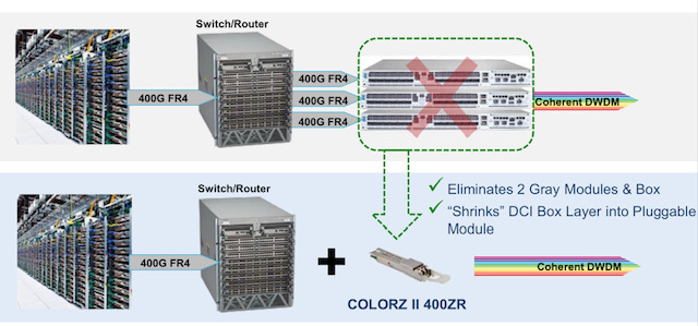
For Verizon Media’s trial, the ColorZ II 400ZR QSFP-DD was added to switches from Arista Networks. Using ColorZ II optics in the same 100GHz channels quadruples fibre capacity from 4 to 16 terabits while halving the transmission cost-per-bit.
Nitin Batta, principal infrastructure architect at Verizon Media, said in a press release that the ColorZ II was chosen to enable it to “rapidly, easily and cost-effectively add terabits of capacity in response to customer demand.”
The 400ZR standard ensures interoperability and gives customers confidence by having several module companies to choose from, says Maj. Adopting the module also provides important diagnostic information regarding a link’s performance.
All the elements for a 400-gigabit ecosystem are coming together, says Inphi.
Four-hundred-gigabit client-side optical modules are leading the way and now 400-gigabit coherent pluggables are at the testing and validation stage before volume deployment.
The ColorZ II will be generally available at the year’s end.

Telecoms' innovation problem and its wider cost
Imagine how useful 3D video calls would have been this last year.
The technologies needed – a light field display and digital compression techniques to send the vast data generated across a network – do exist but practical holographic systems for communication remain years off.
But this is just the sort of application that telcos should be pursuing to benefit their businesses.
A call for innovation
“Innovation in our industry has always been problematic,” says Don Clarke, formerly of BT and CableLabs and co-author of a recent position paper outlining why telecoms needs to be more innovative.
Entitled Accelerating Innovation in the Telecommunications Arena, the paper’s co-authors include representatives from communications service providers (CSPs), Telefonica and Deutsche Telekom.
In an era of accelerating and disruptive change, CSPs are proving to be an impediment, argues the paper.
The CSPs’ networking infrastructure has its own inertia; the networks are complex, vast in scale and costly. The operators also require a solid business case before undertaking expensive network upgrades.
Such inertia is costly, not only for the CSPs but for the many industries that depend on connectivity.
But if the telecom operators are to boost innovation, practices must change. This is what the position paper looks to tackle.
NFV White Paper
Clarke was one of the authors of the original Network Functions Virtualisation (NFV) White Paper, published by ETSI in 2012.
The paper set out a blueprint as to how the telecom industry could adopt IT practices and move away from specialist telecom platforms running custom software. Such proprietary platforms made the CSPs beholden to systems vendors when it came to service upgrades.

The NFV paper also highlighted a need to attract new innovative players to telecoms.
“I see that paper as a catalyst,” says Clarke. “The ripple effect it has had has been enormous; everywhere you look, you see its influence.”
Clarke cites how the Linux Foundation has re-engineered its open-source activities around networking while Amazon Web Services now offers a cloud-native 5G core. Certain application programming interfaces (APIs) cited by Amazon as part of its 5G core originated in the NFV paper, says Clarke.
Software-based networking would have happened without the ETSI NFV white paper, stresses Clarke, but its backing by leading CSPs spurred the industry.
However, building a software-based network is hard, as the subsequent experiences of the CSPs have shown.
“You need to be a master of cloud technology, and telcos are not,” says Clarke. “But guess what? Riding to the rescue are the cloud operators; they are going to do what the telcos set out to do.”
For example, as well as hosting a 5G core, AWS is active at the network edge including its Internet of Things (IoT) Greengrass service. Microsoft, having acquired telecom vendors Metaswitch and Affirmed Networks, has launched ‘Azure for Operators’ to offer 5G, cloud and edge services. Meanwhile, Google has signed agreements with several leading CSPs to advance 5G mobile edge computing services.
“They [the hyperscalers] are creating the infrastructure within a cloud environment that will be carrier-grade and cloud-native, and they are competitive,” says Clarke.
The new ecosystem
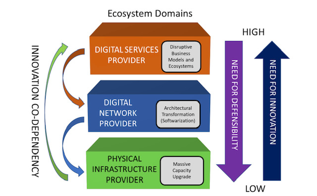
The position paper describes the telecommunications ecosystem in three layers (see diagram).
The CSPs are examples of the physical infrastructure providers (bottom layer) that have fixed and wireless infrastructure providing connectivity. The physical infrastructure layer is where the telcos have their value – their ‘centre of gravity’ – and this won’t change, says Clarke.
The infrastructure layer also includes the access network which is the CSPs’ crown jewels.
“The telcos will always defend and upgrade that asset,” says Clarke, adding that the CSPs have never cut access R&D budgets. Access is the part of the network that accounts for the bulk of their spending. “Innovation in access is happening all the time but it is never fast enough.”
The middle, digital network layer is where the nodes responsible for switching and routing reside, as do the NFV and software-defined networking (SDN) functions. It is here where innovation is needed most.
Clarke points out that the middle and upper layers are blurring; they are shown separately in the diagram for historical reasons since the CSPs own the big switching centres and the fibre that connect them.
But the hyperscalers – with their data centres, fibre backbones, and NFV and SDN expertise – play in the middle layer too even if they are predominantly known as digital service providers, the uppermost layer.
The position paper’s goal is to address how CSPs can better address the upper two network layers while also attracting smaller players and start-ups to fuel innovation across all three.
Paper proposal
The paper identifies several key issues that curtail innovation in telecoms.
One is the difficulty for start-ups and small companies to play a role in telecoms and build a business.
Just how difficult it can be is highlighted by the closure of SDN-controller specialist, Lumina Networks, which was already engaged with two leading CSPs.
In a Telecom TV panel discussion about innovation in telecoms, that accompanied the paper’s publication, Andrew Coward, the then CEO of Lumina Networks, pointed out how start-ups require not just financial backing but assistance from the CSPs due to their limited resources compared to the established systems vendors.
It is hard for a start-up to respond to an operator’s request-for-proposals that can be thousands of pages long. And when they do, will the CSPs’ procurement departments consider them due to their size?
Coward argues that a portion of the CSP’ capital expenditure should be committed to start-ups. That, in turn, would instill greater venture capital confidence in telecoms.
The CSPs also have ‘organisational inertia’ in contrast to the hyperscalers, says Clarke.
“Big companies tend towards monocultures and that works very well if you are not doing anything from one year to the next,” he says.
The hyperscalers’ edge is their intellectual capital and they work continually to produce new capabilities. “They consume innovative brains far faster and with more reward than telcos do, and have the inverse mindset of the telcos,” says Clarke.
The goals of the innovation initiative are to get CSPs and the hyperscalers – the key digital service providers – to work more closely.
“The digital service providers need to articulate the importance of telecoms to their future business model instead of working around it,” says Clarke.
Clarke hopes the digital service providers will step up and help the telecom industry be more dynamic given the future of their businesses depend on the infrastructure improving.
In turn, the CSPs need to stand up and articulate their value. This will attract investors and encourage start-ups to become engaged. It will also force the telcos to be more innovative and overcome some of the procurement barriers, he says.
Ultimately, new types of collaboration need to emerge that will address the issue of innovation.
Next steps
Work has advanced since the paper was published in June and additional players have joined the initiative, to be detailed soon.
“This is the beginning of what we hope will be a much more interesting dialogue, because of the diversity of players we have in the room,” says Clarke. “It is time to wake up, not only because of the need for innovation in our industry but because we are an innovation retardant everywhere else.”
Further information:
Telecom TV’s panel discussion: Part 2, click here
Tom Nolle’s response to the Accelerating Innovation in the Telecommunications Arena paper, click here

Nokia shares its vision for cost-reduced coherent optics
Nokia explains why coherent optics will be key for high-speed short-reach links and shares some of its R&D activities. The latest in a series of articles addressing what next for coherent.
Part 3: Reducing cost, size and power
Coherent optics will play a key role in the network evolution of the telecom and webscale players.
The modules will be used for ever-shorter links to enable future cloud services delivered over 5G and fixed-access networks.
The first uses will be to link data centres and support traffic growth at the network edge.
This will be followed with coherent optics being used within the data centre, once traffic growth requires solutions that 4-level pulse-amplitude modulation (PAM4) direct-detect optics can no longer address.
“If you look at PAM4 up to 100 gigabit for long reach and extended reach optics – distances below 80km – it does not scale to higher data rates,” says Marc Bohn, part of product management for Nokia’s optical subsystem group. ”It only scales if you use 100-gigabit in parallel.”
However, to enable short-reach coherent optics, its cost, size and power consumption will need to be reduced significantly. Semiconductor packaging techniques will need to be embraced as will a new generation of coherent digital signal processors (DSPs).
Capacity growth
The adoption of network-edge and on-premise cloud technologies are fueling capacity growth, says Tod Sizer, smart optical fabric & devices research lab leader at Nokia Bell Labs.
Nokia says capacity growth is at 50 per cent per annum and is even faster within the data centre; for every gigabyte entering a data centre, ten gigabytes are transported within the data centre.
“All of this is driving huge amounts of growth in optical capacity at shorter distances,” says Sizer. “To meet that [demand], we need to have coherent solutions to take over where PAM-4 stops.”
Sizer oversees 130 engineers whose research interests include silicon photonics, coherent components and coherent algorithms.
Applications
As well as data centre interconnect, coherent optics will be used for 5G, access and cable networks; markets also highlighted by Infinera and Acacia Communications.

Nokia says the first driver is data centre interconnect.
The large-scale data centre operators triggered the market for 80-120km coherent pluggables with the 400ZR specification for data centre interconnect.
“Right now, with the different architectures in data centres, these guys are saying 80-120km may be an overshoot, maybe we need something for shorter distances to be more efficient,” says Bohn. “Certainly, coherent can tackle that and that is what we are preparing for because there is no alternative, only coherent can cover that space.”
5G is also driving the need for greater bandwidth.
“Traditionally a whole load of processing has been done at the remote ratio head but increasingly, for cost and performance reasons, people are looking at pulling the processing back into the data centre,” says Sizer.
Another traffic driver is how each cellular antenna has three sectors and can use multiple frequency bands.
“Some research we are looking at requires 400 gigabits and above,” says Sizer. “If you want to do a full [mobile] front haul for a massive MIMO (multiple input, multiple output) array, for example.”
Challenges
Several challenges need to be overcome before coherent modules are used widely for shorter-reach links.
To reduce coherent module cost, the optics and DSP need to be co-packaged, borrowing techniques developed by the chip industry.
“Optical and electrical should be brought close together,” says Bohn. “[They should be] co-designed and co-packaged, and the ideal candidate for that is to combine silicon photonics and the DSP.”
The aim is to turn complex designs into a system-on-chip. “Both [the DSP and silicon photonics] are CMOS and you can apply 2D and 3D [die] stacking multi-chip module techniques,” says Bohn, who contrasts it with the custom and manual manufacturing techniques used today.
The coherent DSP also needs to be much simpler than the high-end DSPs used for long-distance optical transport.
For example, the dispersion compensation, which accounts for a significant portion of the chip’s circuitry, is less demanding for shorter links. The forward-error-correction scheme used can also be relaxed as can the bit precision of the analogue-to-digital and digital-to-analogue converters.
Nokia can co-design the silicon photonics and the DSP following its acquisition of Elenion. Nokia is also exploiting Elenion’s packaging know-how and the partnerships it has developed.
Inside the data centre
Nokia highlights two reasons why coherent will eventually be used within the data centre.
The first is the growth in capacity needed inside the data centre. “For the same reason we believe coherent will be the right solution for data centre interconnect and access, the same argument can be made within the data centre,” says Sizer.
A campus data centre is distributed across several buildings and linking them is driving a need for 400-gigabit lanes or more.
This requires a ZR-like solution but for 2km or so rather than 80km.
“It is one of the solutions certainly but that will be driven an awful lot by whether we can make cost-effective solutions to meet the cost targets of the data centre,” says Sizer. That said, there are other ways this can be addressed such as adding fibre.
“Having parallel systems is another area of ongoing research,” says Sizer. “We may need to have unique solutions if traffic grows faster inside the data centre than outside such as spatial-division multiplexing as well as coherent.”
The use of coherent interfaces for networking inside the data centre will take longer.
Bohn points out that 51.2-terabit and 102.4-terabit switches will continue to be served using direct-detect optics but after that, it is unclear because direct-detect optics tops out at 100-gigabits or perhaps 200-gigabits per lane.
“With coherent, it is much easier to get to higher data rates especially over shorter distances,” says Bohn.
Another development benefitting the use of coherent is the next Ethernet standard after 400 Gigabit Ethernet (GbE).
“My research team is looking at that and, in particular, 1.6 Terabit Ethernet (TbE) which is fairly out in the future,” says Sizer. “It will demand a coherent solution, as I expect 800GbE will as well.”
Work to define the next Ethernet standard is starting now and will only be completed in 2025 at the earliest.

Acacia targets access networks with coherent QSFP-DD

- Acacia Communications has announced a 100-gigabit coherent QSFP-DD pluggable module.
- The module is the first of several for aggregation in the access network.
The second article addressing what next for coherent
Part 2: 100-gigabit coherent QSFP-DD
Acacia Communications has revisited 100-gigabit coherent but this time for access rather than metro networks.
Acacia’s metro 100-gigabit coherent pluggable product, a CFP, was launched in 2014. The pluggable has a reach from 80km to 1,200km and consumes 24-26W.
The latest coherent module is the first QSFP-DD to support a speed lower than the 400-gigabit 400ZR and ZR+ applications that have spurred the coherent pluggable market.
The launching of a 100-gigabit coherent QSFP-DD reflects a growing need to aggregate 10 Gigabit Ethernet (GbE) links at the network edge as 5G and fibre are deployed.
“The 10GbE links in all the different types of access networks highlight a need for a cost-effective way to do this aggregation,” says Tom Williams, vice president of marketing at Acacia.
Why coherent?
The deployment of 5G, business services, 10-gigabit passive optical networking (PON) and distributed access architecture (DAA) are driving greater traffic at the network edge.
Direct-detection optics is the main approach used for aggregation but Acacia argues coherent is now a contender.
Until now, Acacia has only been able to offer coherent metro products for access. The company believes a 100-gigabit coherent module is timely given the network edge traffic growth coupled with the QSFP-DD form factor being suited for the latest aggregation and switch platforms. Such platforms are not the high-capacity switches used in data centres yet port density still matters.
“We think we can trigger a tipping point and drive coherent adoption for these applications,” says Williams.
Using coherent brings robustness long associated with optical transport networks. “You just plug both ends in and it works,” he says.
In access, the quality of fibre in the network varies. With coherent, there is no need for an engineer to do detailed characterisations of the link thereby benefiting operational costs.
Adopting coherent technology for access also provides a way to scale. “You may only need 100 gigabits today but there is a clear path to 200 and 400 gigabit and the use of DWDM [dense wavelength-division multiplexing],” says Williams.
100-gigabit QDFP-DD
Acacia’s 100-gigabit QSFP-DD uses a temperature-controlled fixed laser and has a reach of 120km. The 120km span may rarely be needed in practice – up to 80km will meet most applications – but the extra margin will accommodate any vagaries in links.
The module uses Acacia’s 7nm CMOS low-power Greylock coherent digital signal processor (DSP). The Greylock is Acacia’s third-generation low power DSP chip that is used for its 400ZR and ZR+ modules.
The 100-gigabit QSFP-DD shares the same packaging as the 400ZR and ZR+ modules. The DSP, silicon-photonics photonic integrated circuit (PIC), modulator driver and trans-impedance amplifier (TIA) are all assembled into one package using chip-stacking techniques, what Acacia calls an opto-electronic multi-chip module (OEMCM).
“Everything other than the laser is in a single package,” says Williams. “The more we make optics look like electronics and the fewer interconnect points we have, the higher the reliability will be.”
The packaging approach brings size and optical performance benefits. The optics and DSP must be tightly coupled to ensure signal integrity as the symbol rates go up for 400-gigabit and soon 800-gigabit data rates. But this is less of an issue at 100-gigabit given the symbol rate is 32-gigabaud only.
Opportunities
The 100-gigabit QSFP-DD is now sampling and undergoing qualification. Acacia has yet to announce its general availability.
The company is planning other coherent modules for access including a tunable laser-based QSFP-DD as well as designs that meet various environmental requirements.
“We view coherent as moving into the access market and that will require solutions that address the entire market,” says Williams. That said, Acacia admits uncertainty remains as to how widely coherent will be adopted.
“The market has to play out and there are other competitive solutions,” says Williams. “We believe coherent will be the right solution but how that plays out near- to mid-term is uncertain.”
Inphi unveils first 800-gigabit PAM-4 signal processing chip
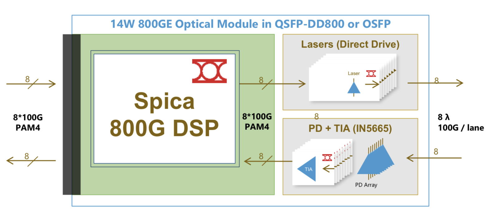
Inphi has detailed what it claims is the industry’s first digital signal processor (DSP) chip family for 800-gigabit client-side pluggable modules.
Dubbed Spica, the 4-level pulse-amplitude modulation (PAM-4) DSP family is sampling and is in the hands of customers.
The physical-layer company has also announced its third-generation Porrima family of PAM-4 DSPs for 400-gigabit pluggables.
The Porrima DSP with integrated laser driver has being made using a 7nm CMOS process; until now a 16nm CMOS has been used. Fabricating the chip using the more advanced process will reduce the power consumption of 400-gigabit module designs.
Applications
Eight-hundred-gigabit multi-source agreements (MSAs) will enable a new generation of high-speed optical transceivers to come to market.
The 800G Pluggable MSA developing optical specifications for 800-gigabit pluggable modules, is one that Inphi is promoting, while the QSFP-DD800 MSA is extending the double density form factor for 800 gigabits.

The main two markets driving a need for 800-gigabit modules are artificial intelligence (AI) and data centre switching, says Eric Hayes, senior vice president, networking interconnect at Inphi.
“AI, while still in its infancy, has all these applications and workloads that it can drive,” he says. “But one thing they have in common when we look at the data centres building large AI clusters is that they have very large data sets and lots of data flow.”
The speed of the input-output (I/O) of the AI processors used in the clusters is rising to cope with the data flows.
The second application that requires 800-gigabit modules is the advent of 25.6-terabit Ethernet switches used to network equipment within the data centre.
Inphi says there are two types of 25.6-terabit switch chips emerging: one uses 50-gigabit PAM-4 while the second uses 100-gigabit PAM-4 electrical interfaces.
“The 25.6-terabyte switch with 100-gigabit I/O is wanted for one-rack-unit (1RU) platforms,” says Hayes. “To do that, you need an 800-gigabit module.” Such switches have yet to reach the marketplace.
The first-generation AI processors used 25-gigabit non-return-to-zero (NRZ) signalling for the I/O while many of the devices shipping today use 50-gigabit PAM-4. “The latest designs that are coming to market have 100-gigabit I/O and we have the first DSP offering 100-gigabit on the host side,” says Hayes.
Spica and Porrima ICs
The Spica DSP takes 100-gigabits PAM-4 electrical signals from the host and performs retiming and pre-emphasis to generate the 100-gigabit PAM-4 signals used for modulation the optics before transmission. The laser driver is integrated on-chip.
The transmit path is a simpler design than the Porrima in that the signalling rate is the same at the input and the output. Accordingly, no gearbox circuitry is needed.
The main signal processing is performed at the receiver to recover the sent PAM-4 signals. A hybrid design is used combining analogue and digital signal processing, similar to the design used for the Porrima.
The Spica device supports 2×400-gigabit or 8×100-gigabit module designs and enables 800-gigabit or 8×100-gigabit optical interconnects. The 800-gigabit form factors used are the QSFP-DD800 and the OSFP. Inphi says both designs consume under 14W.
“The first module being built [using the Spica] is the OSFP because the end-user is demanding that, but we also have customers building QSFP-DDs,” says Hayes.
Meanwhile, Inphi’s Porrima family of devices is targeted at the 400G DR4 and 400G FR4 specifications as well as 100-gigabit module designs that use 100-gigabit PAM-4.
The two module types can even be combined when a 400-gigabit pluggable such as a QSFP-DD or an OSFP is used in breakout mode to feed four 100-gigabit modules implement using such form factors as the QSFP, uQSFP or SFP-DD.
Transitioning the Porrima to a 7nm process saves 1.5W of power, says Hayes, resulting in an 8W 400-gigabit module. The latest Porrima is sampling and is with customers.
Roadmap
Inphi says optical modules using the Spica DSP will be deployed in volume from the second half of 2021.
Before then, the DSP will be tested as part of customers’ module designs, then be integrated with the software before the complete 800-gigabit module is tested.
“There will then be interoperability testing between the modules once they become available and then small pilot networks using 800-gigabit modules will be built and tested before the go-ahead to mass deployment,” says Hayes.
All these stages will require at least a year’s work.