
Companies gear up to make 800 Gig modules a reality
Nine companies have established a multi-source agreement (MSA) to develop optical specifications for 800-gigabit pluggable modules.
The MSA has been created to address the continual demand for more networking capacity in the data centre, a need that is doubling roughly every two years. The largest switch chips deployed have a 12.8 terabit-per-second (Tbps) switching capacity while 25.6-terabit and 51-terabit chips are in development.
“The MSA members believe that for 25.6Tbps and 51.2Tbps switching silicon, 800-gigabit interconnects are required to deliver the required footprint and density,” says Maxim Kuschnerov, a spokesperson for the 800G Pluggable MSA.
A 1-rack-unit (1RU) 25.6-terabit switch platform will use 32, 800-gigabit modules while a 51.2-terabit 2RU platform will require 64.
The MSA has been founded now to ensure that there will be optical and electrical components for 800-gigabit modules...
Motivation
The founding members of the 800G MSA are Accelink, China Telecommunication Technology Labs, H3C, Hisense Broadband, Huawei Technology, Luxshare, Sumitomo Electric Industries, Tencent, and Yamaichi Electronics. Baidu, Inphi and Lumentum have since joined the MSA.
The MSA has been founded now to ensure that there will be optical and electrical components for 800-gigabit modules when 51.2-terabit platforms arrive in 2022.
And an 800-gigabit module will be needed rather than a dual 400-gigabit design since the latter will not be economical.
“Historically, the cost of optical short-reach interfaces has always scaled with laser count,” says Kuschnerov. “Pluggables with 8, 10 or 16 lasers have never been successful in the long run.”
He cites such examples as the first 100-gigabit module implemented using 10×10-gigabit channels, and the early wide-channel 400 Gigabit Ethernet designs such as the SR16 parallel fibre and the FR8 specifications. The yield for optics doesn’t scale in the same way as CMOS for parallel designs, he says.
That said, the MSA will investigate several designs for the different reaches. For 100m, 8-channel and 4-channel parallel fibre designs will be explored while for the longer reaches, single-fibre coarse wavelength division multiplexing (CWDM) technology will be used.

Shown from left to right are a PSM8 and a PSM4 module for 100m spans, and the CWDM4 design for 500m and 2km reaches. Source: 800G Pluggable MSA.
“Right now, we are discussing several technical options, so there’s no conclusion as to which design is best for which reach class,” says Kuschnerov.
The move to fewer channels is similar to how 400 Gigabit Ethernet modules have evolved: the 8-channel FR8 and LR8 module designs address early applications but, as demand ramp, they have made way for more economical four-channel FR4 and LR4 designs.
Specification work
The MSA will focus on several optical designs for the 800G Pluggable MSA, all using 112Gbps electrical input signals.
The first MSA design, for applications up to 100m, will explore 8×100-gigabit optical channels as a fast-to-market solution. This is a parallel single-mode 8-channel (PSM8) design, with each 100-gigabit channel carried over a dedicated fibre. The module will use 16 fibres overall: eight for input and eight for output. The MSA will also explore a PSM4 design – ‘the real 800G’ – where each fibre carries 200 gigabits.
The CWDM designs, for 500m and 2km, will require a digital signal processor (DSP) to implement four-level pulse-amplitude modulation (PAM4) signalling that generates the 200-gigabit channels. An optical multiplexer and demultiplexer will also be needed for the two designs.

The MSA will explore the best technologies for each of the three spans. The modulation technologies to be investigated include silicon photonics, directly modulated lasers (DML) and externally modulated lasers (EML).
Challenges
The MSA foresees several technical challenges at 800 gigabits.
One challenge is developing 100-gigabaud direct-detect optics needed to generate the four 200 gigabit channels using PAM4. Another is fitting the designs into a QSFP-DD or OSFP pluggable module while meeting their specified power consumption limitations. A third challenge is choosing a low-power forward error correction scheme and a PAM4 digital signal processor (DSP) that meet the MSA’s performance and latency requirements.
“We expect first conclusions in the fourth quarter of 2020 with the publication of the first specification,” says Kuschnerov.
The 800G Pluggable MSA is also following industry developments such as the IEEE proposal for the 8×100-gigabit SR8 over multi-mode fibre that uses VCSELs. But the MSA believes VCSELs represent a higher risk.
“Our biggest challenge is creating sufficient momentum for the 800-gigabit ecosystem, and getting key industry contributors involved in our activity,” says Kuschnerov.
Arista Networks, the switch vendor that has long promoted 800-gigabit modules, says it has no immediate plans to join the MSA.
“But as one of the supporters of the OSFP MSA, we are aligned in the need to develop an ecosystem of technology suppliers for components and test equipment for OSFP pluggable optics at 800 gigabits,” says Martin Hull, Arista’s associate vice president, systems engineering and platforms.
Hull points out that the OSFP pluggable module MSA was specified with 800 gigabits in mind.
Next-generation Ethernet
The fact that there is no 800 Gigabit Ethernet standard will not hamper the work, and the MSA cannot wait for the development of such a standard.
“The IEEE is in the bandwidth assessment stage for beyond 400-gigabit rates and we haven’t seen too many contributions,” says Kuschnerov. The IEEE would then need to start a Call For Interest and define an 800GbE Study Group to evaluate the technical feasibility of 800GbE. Only then will an 800GbE Task Force Phase start. “We don’t expect the work on 800GbE in IEEE to progress in line with our target for component sampling,” says Kuschnerov. First prototype 800G MSA modules are expected in the fourth quarter of 2021.
Arista’s Hull stresses that an 800GbE standard is not needed given that 800-gigabit modules support standardised rates based on 2×400-gigabit and 8×100-gigabit.
Moreover, speed increments for Ethernet are typically more than 2x. “That would suggest an expectation for 1 Terabit Ethernet (TbE) or 1.6TbE speeds,” says Hull. This was the case with the bandwidth transition from 10GbE to 40GbE (4x), and 40GbE to 100GbE (2.5x).
“It would be unusual for Ethernet’s evolution to slow to a 2x rate and make 800 Gigabit Ethernet the next step,” says Hull. “The introduction of 112Gbps serdes allows for a doubling of input-output (I/O) on a per-physical interface but this is not the next Ethernet speed.”
Pluggable versus co-packaged optics
There is an ongoing industry debate as to when switch vendors will be forced to transition from pluggable optics on the front panel to photonics co-packaged with the switch ASIC.
The issue is that with each doubling of switch chip speed, it becomes harder to get the data on and off the chip at a reasonable cost and power consumption. Driving the ever faster signals from the chip to the front-panel optics is also becoming challenging.
Packaging the optics with the switch chip enables the high-speed serialiser-deserialiser (serdes), the circuitry that gets data on and off the chip, to be simplified; no longer will the serdes need to drive high-speed signals across the printed circuit board (PCB) to the front panel. Adopting co-packaged optics simplifies the PCB design, constrains the switch chip’s overall power consumption given how hundreds of serdes are used, and reduces the die area reserved for the serdes.
But transitioning to co-packaged optics represents a significant industry shift.
The consensus at a panel discussion at the OFC show, held in March, entitled Beyond 400G for Hyperscaler Data Centres, was that the use of front-panel pluggable optics will continue for at least two more generations of switch chips: at 25.6Tbps and at 51.2Tbps.
It is a view shared by the 800G Pluggable MSA and one of its motivating goals.
“The MSA believes that 800-gigabit pluggables are technically feasible and offer clear benefits versus co-packaging,” says Kuschnerov. “As long as the industry can support pluggables, this will be the preferred choice of the data centre operators.”
It has always paid off to bet on the established technology as long as it is technically feasible due to the sheer amount of investment already made, says Kuschnerov.
Major shifts in interconnects such as coherent replacing direct detect, or PSM/ CWDM pushing out VCSELs, or optics replacing copper have happened only when legacy technologies approach their limits and which can’t be overcome easily, he says: “We don’t believe in such fundamental limitations for 800-gigabit pluggables.”
So when will the industry adopt co-packaged optics?
“We believe that beyond 51.2Tbps there is a very high risk surrounding the serdes and thus co-packaging might become necessary to overcome this limitation,” says Kuschnerov.
Switch-chip-maker, Broadcom, has said that co-packaged optics will be adopted alongside pluggables, enabling the hyperscalers to lessen the risk of the new technology’s introduction. Broadcom believes that co-packaged optics solutions will appear as early as the advent of 25.6-terabit switch chips.
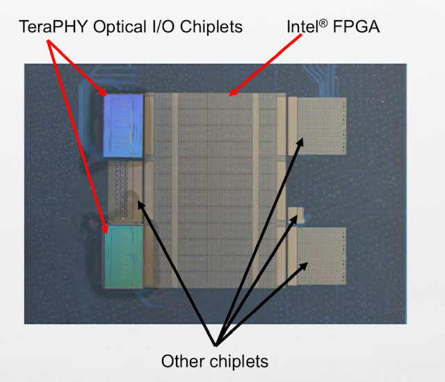
An earlier transitional introduction is also a view shared by Hugo Saleh, vice president of marketing and business development at silicon photonics specialist at Ayar Labs, which recently unveiled its optical I/O chiplet technology is being co-packaged with Intel’s Stratix 10 FPGA.
Saleh says the consensus is that the node past 51.2Tbps must use in-packaged optics. But he also expects overlap before then, especially for high-end and custom solutions.
“It [co-packaged optics] is definitely coming, and it is coming sooner than some folks expect,” says Saleh.
Several companies have contacted the MSA since its 800-gigabit announcement. The 800G MSA is also in discussion with several component and module vendors that are about to join, from Asia and elsewhere. Inphi and Lumentum have joined since the MSA was announced.
Discussions have started with system vendors and hyperscale data center operators; Baidu is one that has since signed up.

Ayar Labs and Intel add optical input-output to an FPGA
Start-up Ayar Labs, working with Intel, has interfaced its TeraPHY optical chiplet to the chip giant’s Stratix10 FPGA.
Hugo SalehIntel has teamed with several partners in addition to Ayar Labs for its FPGA-based silicon-in-package design, part of the US Defense Advanced Research Projects Agency’s (DARPA) project.
Ayar Labs used the Hot Chips conference, held in Palo Alto, California in August, to detail its first TeraPHY chiplet product and its interface to the high-end FPGA.
Origins
Ayar Labs was established to commercialise research that originated at MIT. The MIT team worked on integrating both photonics and electronics on a single die without changing the CMOS process.
The start-up has developed such building-block optical components in CMOS as a vertical coupler grating and a micro-ring resonator for modulation, while the electronic circuitry can be used to control and stabilise the ring resonator’s operation.
Ayar Labs has also developed an external laser source that provides an external light source that can power up to 256 optical channels, each operating at either 16, 25 or 32 gigabits-per-second (Gbps).
The company has two strategic investors: Intel Capital, the investment arm of Intel, and semiconductor firm GlobalFoundries.
The start-up received $24 million in funding late last year and has used the funding to open a second office in Santa Clara, California, and double its staff to about 40.
Markets
Ayar Labs has identified four markets for its silicon photonics technology.
The first is the military, aerospace and government market segment. Indeed, the Intel FPGA system-in-package is for a phased-array radar application.
Two further markets are high-performance computing and artificial intelligence, and telecommunications and the cloud.
Computer vision and advanced driver assisted systems is the fourth market segment. Here, the start-up’s expertise in silicon photonics is not for optical I/O but a sensor for LIDAR, says Hugo Saleh, Ayar Labs’ vice president of marketing and business development.
Stratix 10 system-in-package
The Intel phased-array radar system-in-package is designed to takes in huge amounts of RF data that is down-converted and digitised using an RF chiplet. The data is then pre-processed on the FPGA and sent optically using Ayar Labs’ TeraPHY chiplets for further processing in the cloud.
“To digitise all that information you need multiple TeraPHY chiplets per FPGA to pull the information back into the cloud,” says Saleh. A single phased-array radar can use as many as 50,000 FPGAs.
Such a radar design can be applied to civilian and to military applications where it can track 10,000s of objects.
Moreover, it is not just FPGAs that the TeraPHY chiplet can be interfaced to.
Large aerospace companies developing flight control systems also develop their own ASICs. “Almost every single aerospace company we have talked to as part of our collaboration with Intel has said they have custom ASICs,” says Saleh. “They want to know how they can procure, package and test the chiplets and bring them to market.”
It is one thing to integrate a chiplet but photonics is tricky
TeraPHY chiplet
Two Intel-developed technologies are used to interface the TeraPHY chiplet to the Stratix 10 FPGA.
The first is Intel’s Advanced Interface Bus (AIB), a parallel electrical interface technology. The second is the Embedded Multi-die Interconnect Bridge (EMIB) which supports the dense I/O needed to interface the main chip, in this case, the FPGA to a chiplet.
EMIB is a sliver of silicon designed to support I/O. The EMIBs are embedded in an organic substrate on which the dies sit; one is for each chiplet-FPGA interface. The EMIB supports various bump pitches to enable dense I/O connections.
Ayar Labs’ first TeraPHY product uses 24 AIB cells for its electrical interface. Each cell supports 20 channels, each operating at 2Gbps. The result is that each cell supports 40Gbps and the overall electrical bandwidth of the chiplet is 960 gigabits.
The TeraPHY’s optical interface uses 10 transmitter-receiver pairs, each pair supporting 8 optical channels that can operate at 16Gbps, 25Gbps or 32Gbps. The result is that the TeraPHY support a total optical bandwidth ranging from 1.28Tbps to 2.56Tbps.
The optical bandwidth is deliberately higher than the electrical bandwidth, says Saleh: “Just because you have ten [transmit/ receive] macros on the die doesn’t mean you have to use all ten.”
Also, the chiplet supports a crossbar switch that allows one-to-many connections such that an electrical channel can be sent out on more than one optical interface and vice versa.
For the Intel FPGA system-in-package, two TeraPHY chiplets are used, each supporting 16Gbps channels such that the chiplet’s total optical I/O is up to 5.12 terabits.
Ramifications
Saleh stresses the achievement in integrating optics in-package: “It is one thing to integrate a chiplet but photonics is tricky.”
Ayar Labs flip-chips its silicon and etches on the backside. “Besides all the hard work that goes into figuring how to do that, and keeping it hermetically sealed, you still have to escape light,” he says. “Escaping light out of the package that is intended to be high volume requires significant engineering work.” This required working very closely with Intel’s packaging department.
Now the challenge is to take the demonstrator chip to volume manufacturing.
Saleh also points to a more fundamental change that will need to take place with the advent of chip designs using optical I/O.
Over many years compute power in the form of advanced microprocessors that incorporate ever more CPU cores has doubled every two years or so. In contrast, I/O has advanced at a much slower pace – 5 or 10 per cent annually.
This has resulted in application software for high-performance computing being written to take this BW-compute disparity into account, reducing the number of memory accesses and minimising I/O transactions.
“Software now has to be architected to take advantage of all this new performance and all this new bandwidth,” he says. “We are going to see tremendous gains in performance because of it.”
Ayar Labs says it is on schedule to deliver its first TeraPHY chiplet product in volume to lead customers by the second half of 2020.

Infinera unveils first platforms using its latest PIC & DSP

- The Cloud Xpress 2 platform for data centre interconnects packs 1.2 terabits in a 1 rack unit (1RU) box.
- Infinera has also unveiled two DTN-X XT ‘meshponder’ platforms that aggregate client signals and offer sliceable transponder functionality that delivers wavelengths to multiple destinations.
- The company also announced an open flexible grid line system that supports the C and L bands
- Three of the top four US internet content providers are Infinera customers.
Infinera has started to unveil its platform portfolio based on its Infinite Capacity Engine that combines the company’s latest-generation photonic integrated circuit (PIC) and coherent DSP-ASIC technology.
The first platform using the technology is the Cloud Xpress 2, Infinera second-generation data centre interconnect platform, was unveiled in September. More recently, it has added two DTN-X meshponder platforms – the XT-3300 and the XT-3600 – as well as upgrading two of its existing DTN-X platforms.
“It is impressive that Infinera has turned its Infinite Capacity Engine into products fairly quickly,” says Sterling Perrin, senior analyst at Heavy Reading.
Cloud Express 2
The Cloud Xpress 2 uses a PIC that supports six wavelengths, each transmitting at 200 gigabits-per-second (Gbps) using polarisation-multiplexed, 16 quadrature amplitude modulation (PM-16QAM).
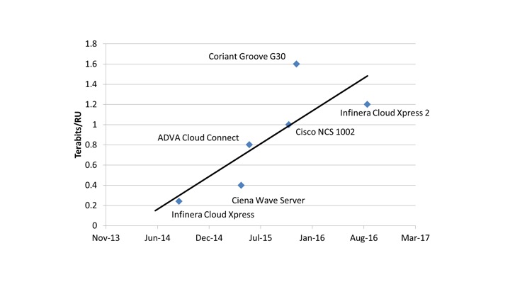
According to Infinera, the 1.2-terabit Cloud Xpress 2 is a 1 rack unit (1RU) box can be stacked to deliver a total of 27.6 terabits of capacity using the C-band. The platform also consumes the equivalent of 0.57W-per-gigabit, half the power consumption of the Cloud Xpress that was launched in 2014.
Infinera was the first vendor to unveil a specific product for data centre interconnect when it launched the Cloud Xpress, says Perrin. “Then everyone else came out with products that were not PIC-based, each one leapfrogging the others,” he says. “So Infinera had to do something with the Cloud Xpress because it was falling behind.”
Now, with the Cloud Xpress 2, Infinera is once again at the leading edge of platform performance for data centre interconnect.
The Cloud Xpress 2 also includes integrated multiplexing and amplification. Geoff Bennett, director, solutions and technology at Infinera, points out that competitor data centre interconnect platforms that use CFP2-ACO optical modules have wavelength outputs that need to be multiplexed onto fibre whereas Infinera’s PIC has a single fibre-pair output. The platform also integrates amplification to enable a reach of up to 130km without requiring external line amplification, an important requirement for data centre operators. Using line amplification, the Cloud Xpress 2 has a reach of some 600km.
Infinera’s Infinite Capacity Engine supports up to 12 wavelengths and a range of modulation schemes including PM-16QAM but the company has chosen to use six wavelengths rather than the full 12-wavelength PIC for the Cloud Xpress 2.
The Cloud Xpress 2 already delivers a 4.8x improvement in line-side capacity density compared to the Cloud Xpress, explains Bennett. The Cloud Xpress 2 supports 1.2 terabits in 1RU rack compared to 500 gigabits in the 2RU Cloud Xpress box. “That is already a big jump,” says Bennett.
“We have to see what happens next year. Is everybody else going to come out with round-two products using conventional optics that go ahead of the Cloud Xpress 2? Or is the Infinera platform cemented in there at the leading edge?
There is also an economic consideration in terms of how much bandwidth the compact data centre interconnect platform delivers. Cloud Xpress 2 delivers 1.2 terabits which may not be fully used when installed, with Infinera only being paid for those wavelengths used. “There are breakeven points – granularity points – that are important with this platform,” says Bennett.
A third consideration is the power consumption. “2.4 terabits [a full 12-wavelength PIC] in a rack unit will probably go way beyond what can be powered and cooled,” says Bennett. “In a data centre, a key thing is the power drawn per rack unit.”
Financial analyst George Notter of Jefferies visited Infinera during a recent analyst day. In a research note, he commented how Infinera has been delivering new product offerings in 4-year cycles. Notter said that while PIC development cycle times are still in the four-year range, Infinera is now working on two generations of PICs concurrently.
Infinera expects its fifth-generation PIC to be generally available in 2018. The PIC should provide up to 9.6 terabits, he says.
This suggests Infinera’s next-generation Cloud Xpress could be launched in two years’ time and would use the fifth-generation PIC rather than the existing Infinite Capacity Engine PIC using all 12 wavelengths.
Perrin says that when the Cloud Xpress was first announced, he thought it proved conclusively that a PIC is best suited for data centre interconnect. But given how rapidly the industry responded with platforms based on conventional optics, he is now unsure.
“We have to see what happens next year,” says Perrin. “Is everybody else going to come out with round-two products using conventional optics that go ahead of the Cloud Xpress 2? Or is the Infinera platform cemented in there at the leading edge?”
Cloud Xpress 2 is expected to be generally available early in 2017.
Web-scale transport
Infinera’s two new DTN-X meshponder platforms, the 1.2-terabit XT-3300 and the 2.4-terabit XT-3600, are designed for longer-reach mesh networks. In effect, the two meshponder platforms have enhanced telecom capabilities compared to the Cloud Xpress 2 designed for data centre interconnect, just as Infinera launched the DTN-X XT-500 muxponder after it first launched the Cloud Xpress.
However, the XT-3300 and XT-3600 platforms reflect the growing influence of data centre traffic as part of the overall traffic carried by networks, says Infinera, such that telecom equipment need to accommodate both traffic types.
Data centre operators must cope with massive increases in capacity demand, says Bennett. Their traffic requirements are made up of single ‘linear’ traffic flows, each occupying the full capacity of an optical channel.
Such flows may be 10 gigabits or increasingly 100-gigabit and are typically point-to-point. “All the classical telco strategies for dealing with over-demand don’t work in such web-scale networks because they have ‘elephant’ flows that can’t be broken up,” says Bennett.
How do you allow telcos to take on cloud architectures but still solve telco problems? And how do you allow web-scale data centre operators to scale out to a network that is telco-grade?
In contrast, telcos must support combinations of many, smaller traffic flows from hundreds or thousands of locations. But as operators start to re-engineer their networks to support technologies such as network function virtualisation and cloud services, they increasingly face the same challenges the data centre operators face, says Infinera.
“This is the nub of the problem in how the intelligent transport layer must evolve to be cloud-scale,” says Bennett. “How do you allow telcos to take on cloud architectures but still solve telco problems? And how do you allow web-scale data centre operators to scale out to a network that is telco-grade?”
Meshponders
Infinera’s XT-3300 is styled on the Cloud Xpress 2. It is a stackable 1.2-terabit line-side 1 rack-unit box that is telco grade: it is NEBS-compliant and is designed to work on a dense WDM open line system. The XT-3300 has a dozen 100 Gigabit Ethernet client side ports and like the Cloud Xpress 2, six wavelengths are used to deliver a total of 1.2 terabits of line-side capacity.
“The XT-3300 is more of a data centre product,” says Bennett. “With the Cloud Xpress, we tend to operate over fairly short distances; the XT-3300 is a souped-up version of that.”
In contrast, the XT-3600, at 4RU, is four times the height of the XT 3300, and at 2.4 terabits supports double the line side capacity by using 12 wavelengths. The platform also supports electronic switching and multiplexing.
Both meshponders supports all the advanced coherent toolkit features that Infinera detailed at the start of the year such as sub-carriers, gain sharing and matrix-enhanced phase-shift keying for long-haul links. Both platforms have a maximum reach of 6,000km.
The XT-3600 works with two existing Infinera DTN-X platforms – the XTC-4 and the XTC-10. Accordingly, these platforms have been given a mid-life upgrade with new Infinite Capacity Engine line cards and higher capacity OTN switching to accommodate the traffic from the faster line cards. The XTC-4’s OTN switching capacity has been upgraded to 4.8 terabits, while the XTC-10 OTN switching capacity is upgraded to 12 terabits.
The two XT platforms are dubbed meshponders. With a traditional muxponder, multiple client signals are aggregated before being sent out on a higher capacity single optical channel. A meshponder extends the concept by allowing multiple client signals sent on optical channels that are sent to multiple destinations (see diagrams).
The muxponder is made possible because Infinera’s PIC is ‘sliceable’, the wavelengths supported by the PIC can be used in different optical channel combinations – single channel and super-channels – such that ROADMs within the network can split the optical channels and route them to their destinations.
“The PIC has been redesigned to allow it to be sliced,” says Bennett. To do this, guard bands are added each side of a channel. As such, a sliceable channel is less spectrally efficient than a super-channel whose constituent wavelengths are packed more closely together as all are sent to one destination.
The line side capacity, either a sliced super-channel or a single super-channel, can be terminated on one of Infinera’s core boxes such as the XTC-4 or XTC-10.
Heavy Reading’s Perrin views the meshponders products as an incremental announcement: using its latest PIC, users now have the ability to go point to multipoint using a network of Infinera’s XT systems. The latest XT platforms will appeal to web-scale companies that have metro reaches or greater, says Perrin: “Infinera has got wholesale providers in Europe that transport big chunks of traffic across a greater distance than the Cloud Xpress 2 can do.”
Infinera expects its fifth-generation PIC to be generally available in 2018. The PIC should provide up to 9.6 terabits
Flexible-grid open line systems
Infinera has also announced the MTC-6 flexible grid open line system platform. Infinera’s current FlexILS line system is the 9-slot MTC-9. “The FlexILS is the industry’s most widely deployed flex-grid line system,” says Bennett.
Infinera has also been working with Lumentum to demonstrate its platforms working with Lumentum’s white box open line system. “We have a lot of experience working with open line systems,” says Bennett. Infinera and Lumentum are also part of the open packet optical transport, part of the Telecom Infra Project (TIP) industry initiative co-founded by Facebook, Deutsche Telecom and SK Telecom.
The MTC-6 flexible open line system occupies 6 slots and uses the same cards as its larger counterpart MTC-9. These boards include FlexROADM cards, EDFA amplifiers, RAMAN amplifiers and gain flatteners. The MTC-6 supports the C and L bands, effectively doubling overall transmission capacity from 25.6 terabits using Infinera’s platforms in the C-band to 51.2 terabits using both bands.
Infinera says three of the top four US internet content providers are using its platforms. “We are in the privileged position of the network architects in those companies telling us what they want,” says Bennett.
The MTC-6 FlexILS open line system is available now. The XT-3300 will be available in the first quarter of 2017 with the remaining platforms scheduled for the second quarter of 2017.