
Marvell’s latest acquisition: switch-chip firm Innovium

- Innovium will be Marvell’s fifth acquisition in four years
Marvell is buying switch-chip maker, Innovium, for $1.1 billion to bolster its revenues from the lucrative data centre market.
The combination of Innovium with Inphi, Marvell’s most recent $10 billion acquisition, will enable the company to co-package optics alongside the high-bandwidth, low-latency switch chips.
Marvell returns to the market to gain a scalable, low-latency architecture
“Inphi has quite a bit of experience shipping silicon photonics with the ColorZ and ColorZ II [modules],” says Nariman Yousefi, executive vice president, automotive, coherent DSP and switch group at Marvell. “And we have programmes inside the company to do co-packaged optics as well.”
Innovium
Innovium’s Teralynx family addresses the needs of large-scale data centres and will complement Marvell’s Prestera switch-chip portfolio that addresses enterprise and carrier applications.
Formed in 2014, Innovium is a private company with a staff of 230, 185 of which are engaged in R&D. The company has also raised a total of $400 million in funding.
Innovium is already shipping its 12.8-terabit Teralynx 7 to a leading cloud provider and expects revenues of $150 million in 2022. And earlier this year, it announced it shipped over 1 million 400-gigabit switch-silicon ports in 2020.
“The top cloud players are the ones that drive most of the revenues,” says Yousefi. “But there is a long list of customers that are engaged with Innovium at different capacities and there are a bunch of Tier-2s [data centre operators].”
Marvell gained the Xpliant programmable switch-chip architecture for the data centre when it acquired Cavium Networks in 2018, says Devan Adams, principal analyst at LightCounting.
But soon after the acquisition, the Xpliant switch chip line was discontinued as Marvell decided to concentrate on expanding its Prestera chip family.
Now Marvell has returned to the market to gain a scalable, low-latency architecture that addresses the needs of the mega data centre players.
“When you think of the overall data centre market and how it is booming, Innovium makes Marvell’s solutions more attractive to the key cloud customers by helping them expand their switch-chip offerings,” says Adams.

Marvell says it was impressed with the Innovium design team and with the Teralynx architecture when assessing the company as a potential buy. “We also liked the fact that customers have validated the architecture and that it is shipping and in live networks,” says Yousefi.
Broadcom dominates the switch-chip market. According to the market research company, 650 Group, Broadcom had 72 per cent of the 50-gigabit serialiser-deserialiser (serdes) cloud-based switch market in the first quarter, 2021, while Innovium had 27 per cent.
The cloud players want a choice of suppliers, not just for procurement reasons but to ensure sufficiently strong suppliers that can address their needs.
This latest acquisition, expected to close before the year-end, will be Marvell’s fifth acquisition in four years.
Marvell acquired Inphi earlier this year and two custom ASIC companies in 2019: Avera Semiconductor, originally the ASIC group of IBM Microelectronics, and Aquantia that has multi-gigabit PHY expertise. A year before that, Marvell acquired Cavium, as mentioned.
Marvell will use its sales force to promote Innovium’s products to a larger customer base including customers using its Prestera switch chips.
Adams also notes that Marvell has a broad supply chain and a strategic relationship with leading foundry TSMC that will benefit Innovium in the making of its chips, especially when semiconductors are currently in short supply.
Switch chip styles
There are two types of Ethernet switch chips. For the mega data centres, what is important is capacity and the chip’s throughput per Watt (gigabit-per-second/ Watt). Cloud players need to move traffic efficiently in the data centre and with a low latency. Such chips have a streamlined packet-processing capability. Examples include Broadcom’s Tomahawk and Innovium’s Teralynx lines.
In contrast, enterprises need to support various networking protocols and that requires a broad feature set and packet-processing capability. Marvell’s Prestera and Broadcom’s Trident portfolios fall into this category.
“It is hard to design one device that addresses both,” says Yousefi. “That is why there are two different architectures, design teams, databases and chips.”
Marvell highlights Innovium’s Teralynx portfolio’s low power and low latency. “Even though the application for these devices is supposed to be streamlined, Innovium has managed to put in programmability features that makes the architecture more flexible,” says Yousefi. “These are important differentiators.”
Innovium’s Teralynx 8 family includes a 7nm CMOS, 25.6-terabit chip with 112 gigabit-per-second (Gbps) serialisers-deserialisers (serdes). “The Teralynx 8 switch chip is in the bring-up phase with customers; it is not shipping in volume yet,” says Yousefi.
A future Teralynx 9 has also been mentioned.
Yousefi confirms there will be a next-generation 51.2-terabit switch chip and devices beyond that; what the next device will be called is to be determined.
The Marvell acquisition will also combine the serdes expertise of Inphi and Innovium. “We are going to help, but right now we can’t really do much as two separate companies,” says Yousefi.
Integration
Yousefi is also definitive about Marvell’s co-packaged optics plans but points out that the adoption of the technology will take time for the whole industry.
The integration of the Innovium team within Marvell will be fine-tuned once the two companies formally merge. At a high-level, the Innovium team will continue to focus on what it does best: the high-capacity product line, says Yousefi.
“The real opportunity is how do you leverage the collective teams’ knowledge and efficiencies, share the best practices, help each other out during peak resource crunches, and release products more efficiently,” he says.
More acquisitions
The Innovium deal follows the likes of Intel buying Barefoot Networks and Nvidia buying networking specialist Mellanox which designs its own switch chips.
For Adams, it was those deals that suggested it was only a question of time before someone bid for Innovium.
Adams admits he has no insight into Marvell’s acquisition plans, but he points to how Marvell had its own server CPU chip, the ThunderX3 chip based on ARM cores, which was cancelled last year. Could Marvell decide to re-enter the market via the acquisition route?
Another potential technology Marvell could acquire is programmable logic. FPGAs are used in the data centre as accelerators. Adams also points out that certain switch vendors have added FPGAs to their platforms for niche applications such as high-frequency trading.
As for artificial intelligence (AI) hardware, Marvell has its own IP and has added hardware blocks for AI as part of it Octean 10 design. So perhaps the buying of an AI chip start-up is less likely for now.
Yousefi does not rule out more Marvell acquisitions. “The industry is all about growth and how you can position yourself to do many things,” he says.
But he stresses it will take Marvell time to absorb the latest acquisitions of Inphi and Innovium: “That is just as important as acquiring the right assets.”

ADVA’s 800-gigabit CoreChannel causes a stir

ADVA’s latest addition to its FSP 3000 TeraFlex platform provides 800-gigabit optical transmission. But the announcement has caused a kerfuffle among its optical transport rivals.
ADVA’s TeraFlex platform supports various coherent optical transport sleds, a sled being a pluggable modular unit that customises a platform’s functionality.
The coherent sleds use Cisco’s (formerly Acacia Communication’s) AC1200 optical engine. Cisco completed the acquisition of Acacia in March.
The AC1200 comprises a 16nm CMOS Pico coherent digital signal processor (DSP) that supports two wavelengths, each up to 600-gigabit, and two photonic integrated circuits (PICs), for a maximum capacity of 1.2 terabits.
The latest sled from ADVA, dubbed CoreChannel, supports an 800-gigabit stream in a single channel.
ADVA states in its press release that the CoreChannel uses “140 gigabaud (GBd) sub-carrier technology” to deliver 800-gigabit over distances exceeding 1,600km.
This, the company says, improves reach by over 50 per cent compared with state-of-the-art 95GBd symbol rate coherent technologies.
It is these claims that have its rivals reacting.
“Despite their claims – they are not using actual digital sub-carriers,” says one executive from a rival optical transport firm, adding that what ADVA is doing is banding two independent 70GBd 400-gigabit wavelengths together and trying to treat that as a single 800-gigabit signal.
“This isn’t necessarily a bad solution for some applications – each network operator can decide that for themselves,” says the executive. However, he stresses that the CoreChannel is not an 800-gigabit single-channel solution and uses 4th generation 16nm CMOS DSP technology rather than the latest 5th generation, 7nm CMOS DSP technology.
A second executive, from another optical transport vendor providing 800-gigabit single-wavelength solutions, adds that ADVA’s claim of 140GBd is too ‘creative’ for a two-lambda solution.
“It’s not a real 800 gigabit. Not that this must be bad, but one should call things as they are,” the spokesperson said. “What matters to the operators is the cost, power consumption, reach and density of a modem; the number of lambdas is more of an internal feature.”
CoreChannel
ADVA confirms it is indeed using Cisco’s Pico coherent DSP to drive two wavelengths, each at 400 gigabits-per-second (Gbps).
“You can say the CoreChannel is a less challenging requirement because we are not driving it [the Pico DSP] to the maximum modulation or constellation complexity,” says Stephan Rettenberger, senior vice president, marketing and investor relations at ADVA. “It is the lower end of what the AC1200 can do.”
Until now the two wavelengths have been combined externally, and have not been integrated from a software or a command-and-control approach.
“The CoreChannel sled is just another addition to the TeraFlex toolbox,” says Rettenberger. “It has one physical line interface that drives an 800Gbps stream using two wavelengths, each one around 70GBd, that are logically and physically combined.”
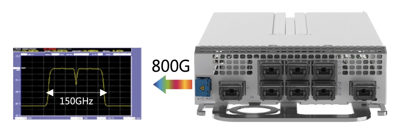
The resulting two-wavelength 800-gigabit stream sits within a 150GHz channel. However, the channel width can be reduced to 125GHz and even 112.5GHz for greater spectral efficiency.
ADVA says the motivation for the design is the customers’ requirement for lower-cost transport and the ability to easily transport 400 Gigabit Ethernet (GbE) client signals.
“With this 800-gigabit line speed, you can go something like 2,000km, that is 50-100 per cent more than what 95GBd single-wavelengths solutions will do,“ says Rettenberger. “And you can also drive it at 400 gigabits and you can do something like 6,000km.”
The reaches quoted are based on a recent field trial involving ADVA.
ADVA uses a single DSP, similar to the latest 800-gigabit systems from Ciena, Huawei and Infinera. Alongside the DSP are two non-hermetically-sealed PICs whereas the 95GBd indium-phosphide solutions use a single hermetically sealed gold box.
ADVA’s solution also requires two lasers whereas the 800-gigabit single-wavelength solutions use one laser.
“Yes, we have two lasers versus one but that is not killing the cost,” says Rettenberger. “And it is also not killing the power consumption because the PIC is so much more power efficient.”
Rettenberger stresses that ADVA is not saying its offering is necessarily a better solution. “But it is a very interesting way to drive 800 gigabits further than these 95 gigabaud solutions,” says Rettenberger. “It has the same cost, space, power efficiency, just greater reach.”
ADVA also agrees that it is not using electrical sub-carriers such as Infinera uses but it is using optical sub-carrier technology.
These two wavelengths are combined logically and also from a physical port interface point of view to fit within a 150GHz window.
The 95GBd, in contrast, is an interim symbol rate step and the resulting 112.5GHz channel width doesn’t easily fit with legacy 25GHz and 50GHz band increments, says ADVA, while the 150GHz band the CoreChannel sled uses is the same channel width that will be used once single-wavelength 140GBd technology becomes available.
Acacia has also long talked about the merit of doubling the baud rate suggesting Cisco’s successor to the AC1200 will have a 140GBd symbol rate. Such a design is expected in the next year or two.
“We feel this [CoreChannel] implementation is already future-proofed,” says Rettenberger.
ADVA says it undertook this development in collaboration with Acacia.
Acacia announced a dual-wavelength single-channel AC1200 solution in 2019. Then, the company unveiled its AC1200-SC2 that delivers 1.2 terabits over an optical channel.
The SC2 (single chip, single channel) is an upgrade of Acacia’s AC1200 module in that it sends 1.2 terabits using two sub-carriers that fit in a 150GHz-wide channel.

Customer considerations
Choosing an optical solution comes down to five factors, each having its weight depending on the network application, says the first executive.
These are capacity-per-wavelength, cost-per-bit, capacity-per- optical-engine or -module, spectral efficiency and hence capacity-per-fibre, and power-per-bit.
“Each is measured for a given distance/ network application,” says the executive. “And the reason the weight changes for different applications is that the importance of each factor is different at different points in the network. For example, the importance of spectral efficiency changes depending on how expensive it is to light up a link (fibre and line system costs).”
For long-haul and submarine, spectral efficiency is the most important factor, while for metro it is typically cost-per-bit. Meanwhile, for data centre interconnect applications, it’s a mix between cost-per-bit and power-per-bit. Capacity-per-wave and capacity-per-optical-engine are valuable because they can reduce the number of wavelengths and modules that need to be deployed, reducing operating expenses and accelerating service activation.
“The reason that 5th generation [7nm CMOS technology] is superior to fourth generation [16nm] DSP technology is that it provides superior performance in every single one of those key criteria,” says the executive. “This fact minimised any potential benefits that could be achieved by banding together two wavelengths using 4th generation technology when compared to a single wavelength using 5th generation technology.”
“It sounds like others feel we have misled the market; that was not the intent,” says Rettenberger.
ADVA does not make its own coherent DSP so it doesn’t care if the chip is implemented using a 16nm, 7nm or a 5nm CMOS process.
“We are trying to build a good solution for transmitting 400GbE signals and, for us, the Pico chip is a wonderful piece of technology that we have now implemented in four different [sled] variants of TeraFlex.”

Turning to optical I/O to open up computing pinch points

Getting data in and out of chips used for modern computing has become a key challenge for designers.
A chip may talk to a neighbouring device in the same platform or to a chip across the data centre.
The sheer quantity of data and the reaches involved – tens or hundreds of meters – is why the industry is turning to optical for a chip’s input-output (I/O).
It is this technology transition that excites Ayar Labs.
The US start-up showcased its latest TeraPHY optical I/O chiplet operating at 1 terabit-per-second (Tbps) during the OFC virtual conference and exhibition held in June.
Evolutionary and revolutionary change
Ayar Labs says two developments are driving optical I/O.
One is the exponential growth in the capacity of Ethernet switch chips used in the data centre. The emergence of 25.6-terabit and soon 51.2-terabit Ethernet switches continue to drive technologies and standards.
This, says Hugo Saleh, vice president of business development and marketing, and recently appointed as the managing director of Ayar Labs’ new UK subsidiary, is an example of evolutionary change.
But artificial intelligence (AI) and high-performance computing have networking needs independent of the Ethernet specification.
“Ethernet is here to stay,” says Saleh. “But we think there is a new class of communications that is required to drive these advanced applications that need low latency and low power.”
Manufacturing processes
Ayar Labs’ TeraPHY chiplet is manufactured using GlobalFoundries’ 45nm RF Silicon on Insulator (45RFSOI) process. But Ayar Labs is also developing TeraPHY silicon using GlobalFoundries’ emerging 45nm CMOS-silicon photonics CLO process (45CLO).
The 45RFSOI process is being used because Ayar Labs is already supplying TeraPHY devices to customers. “They have been going out quite some time,” says Saleh.
But the start-up’s volume production of its chiplets will use GlobalFoundries’ 45CLO silicon photonics process. Version 1.0 of the process design kit (PDK) is expected in early 2022, leading to qualified TeraPHY parts based on the process.
One notable difference between the two processes is that 45RFSOI uses a vertical grating coupler to connect the fibre to the chiplet which requires active alignment. The 45CLO process uses a v-groove structure such that passive alignment can be used, simplifying and speeding up the fibre attachment.
“With high-volume manufacturing – millions and even tens of millions of parts – things like time-in-factory make a big difference,” says Saleh. Every second spent adds cost such that the faster the processes, the more cost-effective and scalable the manufacturing becomes.
Terabit TeraPHY
The TeraPHY chiplet demonstrated during OFC uses eight optical transceivers. Each transceiver comprises eight wavelength-division multiplexed (WDM) channels, each supporting 16 gigabit-per-second (Gbps) of data. The result is a total optical I/O bandwidth of 1.024Tbps operating in each direction (duplex link).
“The demonstration is at 16Gbps and we are going to be driving up to 25Gbps and 32Gbps next,” says Saleh.
The chiplet’s electrical I/O is slower and wider: 16 interfaces, each with 80, 2Gbps channels implementing Intel’s Advanced Interface Bus (AIB) technology.
Last December, Ayar Labs showcased advanced parts using the CLO process. The design was a direct-drive part – a prototype of a future-generation product, not the one demonstrated for OFC.
“The direct-drive part has a serial analogue interface that could come from the host ASIC directly into the ring resonators and modulate them whereas the part we have today is the productised version of an AIB interface with all the macros and all the bandwidth enabled,” says Saleh.
Ayar Labs also demonstrated its 8-laser light source, dubbed SuperNova, that drives the chiplet’s optics.
The eight distributed feedback (DFB) lasers are mixed using a planar lightwave circuit to produce eight channels, each comprising eight frequencies of light.
Saleh compares the SuperNova to a centralised power supply in a server that power pools of CPUs and memory. “The SuperNova mimics that,” he says. “One SuperNova or a 1 rack-unit box of 16 SuperNovas distributing continuous-wave light just like distributed voltage [in a server].”
The current 64-channel SuperNova powers a single TeraPHY but future versions will be able to supply light to two or more.
Ayar Labs is using Macom as its volume supplier of DFB lasers.
Significance
Ayar Labs believes the 1-terabit chip-to-chip WDM link is an industry first.
The demo also highlights how the company is getting closer to a design that can be run in the field. The silicon was made less than a month before the demonstration and was assembled quickly. “It was not behind glass and was operating at room temperature,” says Saleh. “It’s not a lab setting but a production setting.”
The same applies to the SuperNova. The light source is compliant with the Continuous-Wave Wavelength Division Multiplexing (CW-WDM) Multi-Source Agreement (MSA) Group that released its first specification revision to coincide with OFC. The CW-WDM MSA Group has developed a specification for 8, 16, and 32-wavelength optical sources.
The CW-WDM MSA promoter and observer members include all the key laser makers as well as the leading ASIC vendors. “We hope to establish an ecosystem on the laser side but also on the optics,” says Saleh.
“Fundamentally, there is a change at the physical (PHY) level that is required to open up these bottlenecks,” says Saleh. “The CW-WDM MSA is key to doing that; without the MSA you will not get that standardisation.”
Saleh also points to the TeraPHY’s optical I/O’s low power consumption which for each link equates to 5pJ/bit. This is about a tenth of the power consumed by electrical I/O especially when retimers are used. Equally, the reach is up to 2km not tens of centimetres associated with electrical links.
Chiplet demand
At OFC, Arista Networks outlined how pluggable optics will be able to address 102.4 terabit Ethernet switches while Microsoft said it expects to deploy co-packaged optics by the second half of 2024.
Nvidia also discussed how it clusters its graphics processing units (GPUs) that are used for AI applications. However, when a GPU from one cluster needs to talk to a GPU in another cluster, a performance hit occurs.
Nvidia is looking for the optical industry to develop interfaces that will enable its GPU systems to scale while appearing as one tightly coupled cluster. This will require low latency links. Instead of microseconds and milliseconds depending on the number of hops, optical I/O reduces the latency to tens of nanoseconds.
“We spec our chiplet as sub-5ns plus the time of flight which is about 5ns per meter,” says Saleh. Accordingly, the transit time between two GPUs 1m apart is 15ns.
Ayar Labs says that after many conversations with switch vendors and cloud players, the consensus is that Ethernet switches will have to adopt co-packaged optics. There will be different introductory points for the technology but the industry direction is clear.
“You are going to see co-packaged optics for Ethernet by 2024 but you should see the first AI fabric system with co-packaged I/O in 2022,” says Saleh.
Intel published a paper at OFC involving its Stratix 10 FPGA using five Ayar Labs’ chiplets, each one operating at 1.6 terabits (each optical channel operating at 25Gbps, not 16Gbps). The resulting FPGA has an optical I/O capacity of 8Tbps, the design part of the US DARPA PIPES (Photonics in the Package for Extreme Scalability) project.
“A key point of the paper is that Intel is yielding functional units,” says Saleh. The paper also highlighted the packaging and assembly achievements and the custom cooling used.
Intel Capital is a strategic investor in Ayar Labs, as is GlobalFoundries, Lockheed Martin Ventures, and Applied Materials.
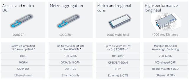
Infinera's XR optics pluggable plans

Infinera’s coherent pluggables for XR optics will also address the company’s metro needs.
Coherent pluggables now dominate the metro market where embedded designs account for just a fifth of all ports, says Infinera.
“As we grow our metro business, we need our own pluggables if we want to be cost-competitive,” says Robert Shore, senior vice president of marketing at Infinera.
Infinera’s family of pluggables implementing the XR optics concept is dubbed ICE-XR.
XR optics splits a coherent optical signal into Nyquist sub-carriers, each carrying a data payload. Twenty-five gigabits will likely be the sub-carrier capacity chosen.
XR optics can be used for point-to-point links where all the sub-carriers go to the same destination. But the sub-carriers can also be steered to different destinations, similar to how breakout cables are used in the data centre.
With XR optics, a module can talk to several lower-speed ones in a point-to-multipoint arrangement. This enables optical feeds to be summed, ideal for traffic aggregation applications such as access and 5G.
Open XR Forum
Infinera detailed its ICE-XR pluggables during the OFC virtual conference and exhibition.
The event coincided with the launch of the Open XR Forum whose members include network operators, Verizon, Lumen Technologies (formerly CenturyLink), Windstream and Liberty Global.
Members of the Open XR Forum span sub-component makers, systems vendors like Infinera, and network operators. The day the Open XR Forum website was launched, Infinera received a dozen enquiries from interested parties.
The Open XR Forum will define standards for XR optics such as how the networks are managed, the form factors used, their speeds and power requirements.
“There are a lot of underlying operational aspects that need to be worked out,” says Shore.
XR optics will use a similar model to ZR+ coherent optics. ZR+ delivers enhanced transmission performance compared to the OIF’s 400ZR coherent standard. “ZR+ is not a standard but rather a set of open specifications that can be used by anyone to create a product, and that is exactly the approach we are taking with XR optics,” says Shore.
Over the last 18 months, Infinera has met with 150 network operators regarding XR optics. “We wanted to validate this is a worthwhile technology and that people wanted it,” says Shore.
There have also been 40 network operator trials of the technology by the end of July. BT has used the technology as part of a metro aggregation trial while Virgin Media and American Tower each tested XR optics over PON.
More members have joined the Open XR Forum and will be announced in the autumn.
ICE-XR
ICE-XR’s name combines two concepts.
The first, ICE, refers to the Infinite Capacity Engine, the optics and coherent digital signal processor (DSP) that is the basis for Infinera’s ICE4 and newer ICE6 coherent transmission designs. ICE4 was Infinera’s first product to use Nyquist sub-carriers.
“XR”, meanwhile, borrows from 400ZR. Here, the ‘X’ highlights that XR supports point-to-point coherent communications, like 400ZR, and point-to-multipoint.
“ICE-XR’s release will be timed in conjunction with the official ratification of the specifications from the Open XR Forum,” says Shore.
Infinera’s ICE-XR portfolio will include 100, 400, and 800-gigabit optical modules.
The 100-gigabit ICE-XR, based on four 25-gigabit sub-carriers, will be offered as QSFP-28, QSDP-DD and CFP2 form factors. The 400-gigabit and 800-gigabit variants, using 16 and 32 sub-carriers respectively, will be available as QSFP-DD and CFP2 modules.
The 100-gigabit and 400-gigabit ICE-XR modules will be released first in 2022.
The 400-gigabit ICE-XR will also double as Infinera’s ZR+ offering when used point-to-point.
Shore says its first ZR+ module will not support the oFEC forward-error correction (FEC) used by the OpenZR+ multi-source agreement (MSA).
“The performance hit you take to ensure multi-vendor interoperability is vastly outweighed by the benefits of the improved [optical] performance [using a proprietary FEC],” says Shore.
Merchant DSP suppliers and the systems vendors with in-house DSP designs all support proprietary FEC schemes that deliver far better performance than oFEC, says Shore.
Infinera is developing a monolithic photonic integrated circuit (PIC) for ICE-XR manufactured at its indium phosphide facility.“ICE-XR will increase the utilisation of our fabrication centre, especially when pluggables produce higher volumes compared to embedded [coherent designs],” says Shore.
Infinera says more than one coherent DSP will be needed for the ICE-XR product portfolio. The modules used have a range of power profiles. The QSFP-28 module will need to operate within 4-5W, for example, while the QSFP-DD implementing ZR+ will need to be below 20W. Developing one DSP to span such a power range is not possible.
Business model
The Open XR Forum’s specifications will enable vendors to develop their own XR optics implementations.
Infinera will also license aspects of its design including its coherent DSPs. The aim, says Shore, is to develop as broad an ecosystem as possible: “We want to make XR optics an industry movement.”
Shore stresses ZR+ interoperability is not a must for most applications. Typically, a vendor’s module will be used at both ends of a link to benefit from the ZR+’s custom features. But interoperability is a must for XR optics given its multi-rate nature. The different speed modules from different vendors must talk to each other.
“Because you have multi-generational and multi-rate designs, it becomes even more important to support multi-vendor interoperability,” says Shore. “It gives the network operators more choice, freedom and flexibility.”
XR optics for the data centre
Infinera says there are developments to use XR optics within the data centre.
As data rates between equipment rise, direct-detect optics will struggle to cope, says Shore. The hierarchical architectures used in data centres also lend themselves to a hub-and-spoke architecture of XR optics.
“This type of technology could fit very nicely into that environment once the capacity requirements get high enough,” says Shore.
For this to happen, power-efficient coherent designs are required. But first, XR optics will need to become established and demonstrate a compelling advantage in a point-to-multipoint configuration.
XR optics will also need to replace traditional direct-detect pluggables that continue to progress; 800-gigabit designs are appearing and 1.6-terabit designs were discussed at OFC. Co-packaged optics is another competing technology.
“You are not looking at the 2022-23 timeframe, but maybe 2025-26,” says Shore.
Covid-era shows
Infinera postponed its customer meetings that pre-covid would take place at OFC till after the show to avoid clashing with the online sessions. Once the meetings occurred, customers were given a tour of Infinera’s virtual OFC booth.
Infinera’s solutions marketing team also divided between them the OFC sessions of interest to attend. The team then ‘met’ daily to share their learnings.
“I do think that the world of in-person events has changed forever,” says Shore. Infinera attended 40 events in 2019. “We will probably do fewer than 20 [a year] going forward,” says Shore.

Nokia adds 400G coherent modules across its platforms

Nokia is now shipping its 400-gigabit coherent multi-haul CFP2-DCO. The module exceeds the optical performance of 400ZR and ZR+ coherent pluggables.
Nokia’s CFP2-DCO product follows its acquisition of silicon photonics specialist, Elenion Technologies, in 2020.
Nokia has combined Elenion’s coherent optical modulator and receiver with its low-power 64-gigabaud (GBd) PSE-Vc coherent digital signal processor (DSP).
Nokia is also adding coherent pluggables across its platform portfolio.
“Not just optical transport and transponder platforms but also our IP routing portfolio as well,” says Serge Melle, director of product marketing, IP-optical networking at Nokia.
“This [amplifier and filter] allows for much better optical performance,”
“This [amplifier and filter] allows for much better optical performance,”
Melle is an optical networking industry veteran. He joined Nokia two years ago after a 15-year career at Infinera. Melle started at Pirelli in 1995 when it was developing a 4×2.5-gigabit wavelength-division multiplexing (WDM) system. In between Pirelli and Infinera, Melle was at Nortel Networks during the optical boom.
400ZR, ZR+ and the multi-haul CFP2-DCO
The CFP2-DCO’s optical performance exceeds that of the QSFP-DD and OSFP form factors implementing 400ZR and ZR+ but is inferior to line-card coherent transponders used for the most demanding optical transport applications.
The 400ZR coherent OIF standard transmits a 400-gigabit wavelength up to 120km linking equipment across data centres. Being a standard, 400ZR modules are interoperable.
The ZR+ adds additional transmission speeds – 100, 200 and 300-gigabits – and has a greater reach than ZR. ZR+ is not a standard but there is the OpenZR+ multi-source agreement (MSA).
Implementing 400ZR and ZR+ coherent modules in a QSFP-DD or OSFP module means they can be inserted in client-side optics’ ports on switches and routers.
The OIF did not specify a form factor as part of the 400ZR standard, says Melle, with the industry choosing the QSFP-DD and OSFP. But with the modules’ limited power dissipation, certain modes of the coherent DSP are turned off, curtailing the feature set and the reach compared to a CFP2-DCO module.
The modules also have physical size restrictions.
“You don’t have enough thermal budget to put an optical amplifier inside the QSFP-DD package,” says Melle. “So you are left with whatever power the DWDM laser outputs through the modulator.” This is -7dBm to -10dBm for 400ZR and ZR+ optics, he says.
The CFP2-DCO is larger such that the DSP modes of encryption, OTN client encapsulation, LLDP snooping (used to gather data about attached equipment), and remote network monitoring (RMON) can be enabled.
The CFP2-DCO can also house an optical amplifier and tunable filter. The filter reduces the out-of-band optical signal-to-noise ratio (OSNR) thereby increasing the module’s sensitivity. “This [amplifier and filter] allows for much better optical performance,” says Melle. A 400-gigabit multi-haul module has a 0dBm optical output power, typically.
The different transceiver types are shown in the table.
Nokia’s paper at the recent OFC virtual conference and exhibition detailed how its 400-gigabit multi-haul CFP2-DCO achieved a reach of 1,200km.
The paper details the transmission of 52, 400-gigabit signals, each occupying a 75GHz channel, for a total capacity of 20.8 terabits-per-second (Tbps).
Melle stresses that the demonstration was more a lab set-up than a live network where a signal goes through multiple reconfigurable optical add-drop multiplexers (ROADMs) and where amplifier stages may not be equally spaced.
That said, the CFP2-DCO’s reach in such networks is 750km, says Nokia.
IP-optical integration
Having coherent pluggables enables 400 Gigabit Ethernet (400GbE) payloads to be sent between routers over a wide area network, says Nokia.
“Given this convergence in form factor, with the QSFP-DD and ZR/ ZR+, you can now do IP-optical integration, putting coherent optics on the router without sacrificing port density or having locked-in ports,” says Melle.
Nokia is upgrading its IP and optical portfolio with coherent pluggables.
“In the routers, ZR/ ZR+, and in transponders not only the high-performance coherent optics – the [Nokia] PSE-Vs [DSP] – but also the CFP2-DCO multi-haul,” says Melle. “The 400-gigabit multi-haul is also going to be supported in our routers.”
Accordingly, Nokia has developed two sets of input-output (I/O) router cards: one supporting QSFP-DDs suited for metro-access applications, and the second using CFP2-DCO ports for metro and regional networks.
The choice of cards adds flexibility for network operators; they no longer need to have fixed CFP2-DCO slots on their router faceplates, whether they are used or not. But being physically larger, there are fewer CFP2-DCO ports than QSFP-DD ports on the I/O cards.
While the QSFP-DD MSA initially defined the module with a maximum power dissipation of 14.5W, a coherent QSFP-DD module consumes 18-20W. Dissipating the heat generated by the modules is a challenge.
Nokia’s airflow cooling is simplified by placing a module on both sides of the line card rather than stacking two CFP2-DCOs, one on top of the other.
Nokia is adding its CFP2-DCO to its 1830 optical transport portfolio. These include its PSI-M compact modular systems, the PSS transponder systems and also its PSS-x OTN switching systems.
The 400ZR/ZR+ module will be introduced with all its routing platforms this summer – the 7250 IXR, 7750 SR, 7750 SR-s, and the 7950 XRS, whereas the CFP2-DCO will be added to its 7750 and 7950 series later this year.
Nokia will source the 400ZR/ZR+ from third parties as well as from its optical networks division.
Its routers use QSFP-DD form-factor for all 400GbE ports and this is consistent for most router vendors in the industry. “Thus, our use and supply of 400ZR/ZR+ pluggable DCOs will focus on the QSFP-DD form-factor,” says Melle. However, the company says it can offer the OSFP form-factor depending on demand.
Network planning study
Nokia published a paper at OFC on the ideal coherent solution for different applications.
For metro aggregation rings with 4-5 nodes and several ROADM pass-throughs, using ZR+ modules is sufficient. Moreover, using the ZR+ avoids any loss in router port density.
For metro-regional core applications, the ZR+’s optical performance is mostly insufficient. Here, the full 400-gigabit rate can not be used but rather 300 gigabit-per-second (Gbps) or even 200Gbps to meet the reach requirements.
Using a 400-gigabit multi-haul pluggable on a router might not match the density of the QSFP-DD but it enables a full 400-gigabit line rate.
For long-haul, the CFP2-DCO’s performance is “reasonable”, says Nokia, and this is where high-performance transponders are used.
What the OFC paper argues is that there is no one-size-fits-all solution, says Melle.
800-Gigabit coherent pluggables
Traditionally, the IEEE has defined short-reach client-side optics while the OIF defines coherent standards.
“If we want this IP-optical convergence continuing in the next generation of optics, those two worlds are going to have to collaborate more closely,” says Melle.
That’s because when a form-factor MSA will be defined, it will need to accommodate the short-reach requirements and the coherent optics. If this doesn’t happen, says Melle, there is a risk of a new split occuring around the IP and optical worlds.
The next generation of coherent pluggables will also be challenging.
All the vendors got together in 2019 and said that 400ZR was just around the corner yet the modules are only appearing now, says Melle.
The next jump in pluggable coherent optics will use a symbol rate of 90-130GBd.
“That is very much the cutting-edge so it brings back the optics as a critical enabling technology, and not just optics but the packaging,” concludes Melle.

SiDx's use of silicon photonics for blood testing
Part 4: Biosensor start-up, SiDx
A blood sample reveals much about a person’s health. But analysing the sample is complicated given its many constituents.
Identifying a user’s blood type is also non-trivial.
If a patient arriving at hospital needs a blood transfusion, the universal donor blood type, O negative, is administered. That’s because it takes too long – 45 minutes typically – to identify the patient’s blood type. This also explains the huge demand for O negative blood.
Identifying blood type promptly is what start-up SiDx set out to address with a platform based on a silicon photonics sensor. The resulting platform does more than just blood-type identification.
SiDx
The Seattle-based start-up was founded in 2017. By then, SiDx had a decade of research behind it, in silicon-photonics biosensors and the associated biochemistry.
SiDx had also started working with a blood centre in Seattle. Such centres source and sell blood to US hospitals.
“We were looking for an application that justified starting the company,” says Jonas Flueckiger, vice president of engineering at SiDx.
Flueckiger notes that silicon photonics is one of several ways to analyse biological materials. “It has advantages but there are alternatives,” he says. “You have to find an application where the advantages of silicon photonics can shine.”
Marketplace and challenges
Flueckiger splits the biosensor marketplace into three: centralised lab equipment, bedside and portable equipment, and home testing.
For centralised labs, what matters is the scale and the ability to perform parallel testing. Here, trained staff are required for sample preparation and operating the equipment.
The second category, bedside and portable systems, are compact and rugged platforms designed to deliver results quickly; SiDx’s testing system takes 12 minutes. Such platforms are newer and are the focus of SiDx and other silicon photonics biosensor start-ups.
“As for home tests, you don’t need a doctor’s office, you can do it yourself,” says Flueckiger.
But medical diagnostics is a challenging market to enter. “The biggest challenge is that it is very, very hard to bring something new into the medical space,” says Flueckiger.
Hospitals are conservative establishments with rigid protocols that have test systems that doctors trust.
“Even though you show your system will be better, more efficient, faster, and the patient will be better served, it is still very hard to make a case to replace existing technology in a hospital,” says Flueckiger.
A new biosensor system must show it saves money, almost as important as demonstrating improved performance. “If your device is better but it costs more, that is not enough,” says Flueckiger.
Even if a start-up develops a system comparable in price, it must displace existing processes. And that raises a series of questions. Who does the testing? Where do the test results go? And who delivers the news to the patient?
“It is a complex picture and it is not just about technology,” says Flueckiger.

Ring resonators
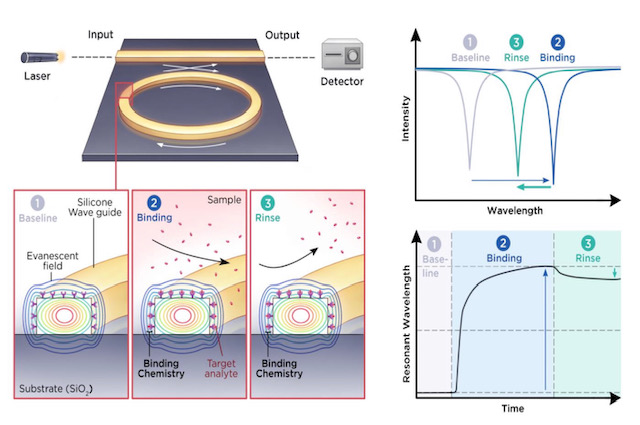
SiDx’s silicon photonics platform measures refractive index changes in light caused by blood sample components attaching to ‘receptors’ placed on the sensor’s surface.
Biochemistry is required to design the receptors for blood analysis and is a core expertise of SiDx.
SiDx uses a laser coupled to a ring resonator. When blood sample constituents attach to the receptors on the ring resonator’s surface, the wavelength at which the sensor resonates changes. This shift in refractive index is used to identify the constituents. (See diagram above.)
A key benefit of the ring resonator approach is its tiny size. Multiple sensors can be integrated into a compact area allowing tests to be performed in parallel. Or as Flueckiger puts it, there is an ability to ask more than one question.
SiDx says it uses ring resonators but it is not detailing its design.
Most emerging integrated-photonics biosensing companies use a laser and ring resonator to read refractive index changes.
One way of get readings is using a tunable laser but alternative designs are possible such as using a fixed laser and tuning the resonator.
That is possible, says Flueckiger, but in a multiplexed design where multiple ring resonators are used, the electrical input-output for all the resonators gets tricky.
“Even for a single test, a single marker, you will have a negative control, a positive control, usually one or two more to make sure you have what you think you have,” says Flueckiger. “With bodily fluids like blood, it is complex and includes stuff that can interfere.”
Silicon photonics also enables label-free detection.
Here, only receptors are used to catch a blood constituent of interest. There is no need for labels with fluorescent attachments designed to link to the constituent.
But labelling improves the probability of identifying what is being looked for. Blood is so complex a sample that doctors may not want label-free testing for just this reason, the risk that another biomarker gives a similar response to what is being sought.
SiDx says sample preparation is key here. Rather than simply squirting the blood sample into the device, additional steps are used such as dilution or separating red blood cells from the serum with testing performed on either. Reagents can also be added to remove all the cells’ membranes.
Such sample preparation steps before label-free testing are important and non-trivial. “Photonics, that is the easy part,” says Flueckiger.
The resulting biosensor comprises optics and biology. Yet it requires a shelf life of 6-12 months. Another reason why medical biosensor design – and the biochemistry in particular – is challenging.
Blood testing and disease screening
Most people understand major blood types such as A, B, AB or O negative, says Flueckiger. But it is more complicated than that in that there are many subgroups. If they are assessed wrongly, it can prove harmful to a patient.
SiDx’s platform can perform blood typing and also Rhesus tests during pregnancy. Rhesus disease is caused by a certain mix of blood types between a pregnant mother and the unborn child.
SiDx sees blood typing as an entry to the market: to prove its technology before branching out. “Once you have blood typing and a sample, you can expand the test portfolio,” says Flueckiger.
The aim is to group tests in an offering that make sense. For example, testing for covid-19 but also testing for the common flu. Or, if a patient tests negative for covid-19, what else could it be? Testing that way and getting an answer avoids the need for a second test.
There are multiple ways to test for covid-19.
A PCR test looks for the DNA of the virus. Analysing a blood sample determines if a body’s immune response has developed antibodies to the virus. If so, it means the person has, or has had, covid-19. SiDx’s biosensor will also be able to test a person’s immune system after a vaccine and determine if a booster jab is needed.
SiDx’s system can detect DNA, but an issue is that DNA needs ‘amplification’; its levels are too small otherwise.
Using integrated photonics coupled with the right capture molecules on the surface allows what is captured to be detected. A DNA molecule is much smaller so other tricks are needed to measure it. As a result, antibodies are more commonly tested for because it is much easier, says Flueckiger.
Prospects
SiDx along with other silicon photonics biosensor companies such as Genalyte, SiPhox, Rockley Photonics and Antelope DX, all received recent funding rounds. SiDx has raised a total of $3 million in funding and $2 million in research funding.
Is this not a vote of confidence in what is a tough market to crack?
There is venture money but it is hard to come by, says Flueckiger. Developing a medical device takes time, a minimum of five years before getting somewhere. If a company starts from scratch, the development time is longer than what venture capitalists are happy with.
Companies pursuing blood testing also can expect greater scrutiny given the story of private company, Theranos, whose claims about developing a breakthrough blood analysis system proved false.
Venture capitalists recognise the potential of benchtop devices but their concern is making money and how quickly a start-up can multiply their investment.
“Unless you can show hockey-stick growth, it’s a tough sell,” says Flueckiger. “These are long-term investments, not like a software company.”
That said, the covid-19 pandemic has helped. People now understand the important role such diagnostic equipment can play. They recognise how long it takes and that if money is thrown at the problem, device development can be accelerated.
Despite the challenges, Flueckiger is upbeat. “We have made lots of progress,” he says. “We have proven to ourselves that our technology works.” SiDx says there are developments that bring its platform closer to market that it cannot disclose at present.
The coronavirus pandemic also provided the company with a motivational boost to launch a product that is far easier to use.
SiDx did consider shifting its focus to address covid-19 testing but the pandemic occurred a year too early. “If it happened now, we would be in a lot better position to turn around very quickly with limited money and have a test ready,” says Flueckiger.
SiDx says that its conversations with investors generate excitement but they want proof of a return.
“You go into this knowing you have a long runway – the next five years will be hard – and then there is the question of whether you will be successful or not,” says Flueckiger.

II-VI expands its 400G and 800G transceiver portfolio

II-VI has showcased its latest high-speed optics. The need for such client-side modules is being driven by the emergence of next-generation Ethernet switches in the data centre.
The demonstrations, part of the OFC virtual conference and exhibition held last month, featured two 800-gigabit and two 400-gigabit optical transceivers.
“We have seen the mushrooming of a lot of datacom transceiver companies, primarily from China, and some have grown pretty big,” says Sanjai Parthasarathi, chief marketing officer at II-VI.
But a key enabler for next-generation modules is the laser. “Very few companies have these leading laser platforms – whether indium phosphide or gallium arsenide, we have all of that,” says Parthasarathi.
During OFC, II-VI also announced the sampling of a 100-gigabit directly modulated laser (DML) and detailed an optical channel monitoring platform.
“We have combined the optical channel monitoring – the channel presence monitoring, the channel performance monitoring – and the OTDR into a single integrated subsystem, essentially a disaggregated monitoring system,” says Parthasarathi.
An optical time-domain reflectometer (OTDR) is used to characterise fibre.
High-speed client-side transceivers
II-VI demonstrated two 800-gigabit datacom products.
One is an OSFP form factor implementing 800-gigabit DR8 (800G-DR8) and the other is a QSFP-DD800 module with dual 400-gigabit FR4s (2x400G-FR4). The DR8 uses eight fibres in each direction, each carrying a 100-gigabit signal. The QSFP-DD800 supports two FR4s, each carrying four, 100-gigabit wavelengths over single-mode fibre.

“These are standard IEEE-compliant reaches: 500m for the DR8 and 2km for the dual FR4 talking to individual FR4s,” says Vipul Bhatt, senior strategic marketing director, datacom at II-VI.
The 800G-DR8 module can be used as an 800-gigabit link or, when broken out, as two 400-gigabit DR4s or eight individual 100-gigabit DR optics.
II-VI chose to implement these two 800-gigabit interfaces based on the large-scale data centre players’ requirements. The latest switches use 25.6-terabit Ethernet chips that have 100-gigabit electrical interfaces while next-generation 51.2-terabit ICs are not far off. “Our optics is just keeping in phase with that rollout,” says Bhatt.
During OFC, II-VI also showcased two 400-gigabit QSFP112 modules: a 400-gigabit FR4 (400G-FR4) and a multi-mode 400-gigabit SR4 (400G-SR4).
The SR4 consumes less power, is more cost-effective but has a shorter reach. “Not all large volume deployments of data centres are necessarily in huge campuses,” says Bhatt.
II-VI demonstrated its 800-gigabit dual FR4 module talking to two of its QSFP112 400-gigabit FR4s.
Bhatt says the IEEE 802.3db standard has two 400G-SR4 variants, one with a 50m reach and the second, a 100m reach. “We chose to demonstrate 100m because it is inclusive of the 50m capability,” says Bhatt.

II-VI stresses its breadth in supporting multi-mode, short-reach single-mode and medium-reach single-mode technologies.
The company says it was the electrical interface rather than the optics that was more challenging in developing its latest 400- and 800-gigabit modules.
The company has 100-gigabit multi-mode VCSELs, single-mode lasers, and optical assembly and packaging. “It was the maturity of the electrical interface [that was the challenge], for which we depend on other sources,” says Bhatt.
100-gigabit PAM-4 DML
II-VI revealed it is sampling a 100-gigabit PAM-4 directly modulated laser (DML).
Traditionally, client-side modules for the data centre come to market using a higher performance indium phosphide externally-modulated laser (EML). The EML may even undergo a design iteration before a same-speed indium phosphide DML emerges. The DML has simpler drive and control circuitry, is cheaper and has a lower power consumption.
“But as we go to higher speeds, I suspect we are going to see both [laser types] coexist, depending on the customer’s choice of worst-case dispersion and power tolerance,” says Bhatt. It is too early to say how the DML will rank with the various worst-case test specifications.
Parthasarathi adds that II-VI is developing 100-gigabit and 200-gigabit-per-lane laser designs. Indeed, the company had an OFC post-deadline paper detailing work on a 200-gigabit PAM-4 DML.
Optical monitoring system
Optical channel monitoring is commonly embedded in systems while coherent transceivers also provide performance metrics on the status of the optical network. So why has II-VI developed a standalone optical monitoring platform?
What optical channel monitors and coherent modules don’t reveal is when a connector is going bad or fibre is getting bent, says Parthasarathi: “The health and the integrity of the fibre plant, there are so many things that affect a transmission.”
Operators may have monitoring infrastructure in place but not necessarily the monitoring of the signal integrity or the physical infrastructure. “If you have an existing network, this is a very easy way to add a monitoring capability,” says Parthasarathi.

“As we can control all the parts – the optical channel monitoring and the OTDR – we can configure it [the platform] to meet the application,” adds Sara Gabba, manager, analysis, intelligence & strategic marcom at II-VI. “Coherent indeed provides a lot of information, but this kind of unit is also suitable for access network applications.”
The optical monitoring system features an optical switch so it can cycle and monitor up to 48 ports.
With operators adopting disaggregated designs, each element in the optical network is required to have more intelligence and more autonomy.
“If you can provide this kind of intelligent monitoring and provide information about a specific link, you create the possibility to be more flexible,” says Gabba.
Using the monitoring platform, intelligence can be more widely distributed in the optical network complementing systems operators may have already deployed, she adds.
Marvell's first Inphi chips following its acquisition

Marvell unveiled three new devices at the recent OFC virtual conference and show.
One chip is its latest coherent digital signal processor (DSP), dubbed Deneb. The other two chips, for use within the data centre, are a PAM-4 (4-level pulse-amplitude modulation) DSP, and a 1.6-terabit Ethernet physical layer device (PHY).
The chips are Marvell’s first announced Inphi products since it acquired the company in April. Inphi’s acquisition adds $0.7 billion to Marvell’s $3 billion annual revenues while the more than 1,000 staff brings the total number of employees to 6,000.
Marvell spends 30 per cent of its revenues on R&D.
Acquisitions
Inphi is the latest of a series of Marvell acquisitions as it focusses on data infrastructure.
Marvell acquired two custom ASIC companies in 2019: Avera Semiconductor, originally the ASIC group of IBM Microelectronics, and Aquantia that has multi-gigabit PHY expertise.
A year earlier Marvell acquired processing and security chip player, Cavium Networks. Cavium had acquired storage specialist, QLogic, in 2017.
These acquisitions have more than doubled Marvell’s staff. Inphi brings electro-optics expertise for the data centre and optical transport and helps Marvell address the cloud and on-premises data centre markets as well as the 5G carrier market.
Marvell is also targeting the enterprise/ campus market and what it highlights as a growth area, automotive. Nigel Alvares, vice president of solutions at Marvell, notes the growing importance of in-vehicle networking, what he calls a ‘data-centre-on-wheels’.
“Inphi’s technology could also help us in automotive as optical technologies are used for self-driving initiatives in future,” says Alvares.
Inphi also brings integration, co-packaging and multi-chip module expertise.

Merchant chip and custom ASIC offerings
Cloud operators and 5G equipment vendors are increasingly developing custom chip designs. Marvell says it is combining its portfolio with their intellectual property (IP) to develop and build custom ICs.
Accordingly, in addition to its merchant chips such as the three OFC-announced devices, Marvell partners with cloud players or 5G vendors, providing them with key IP blocks that are integrated with their custom IP. Marvell can also build the ASICs.
Another chip-design business model Marvell offers is the integration of different hardware in a multi-chip package. The components include a custom ASIC, merchant silicon, high-speed memory and third-party chiplets.
“We co-package and deliver it to a cloud hyperscaler or a 5G technical company,” says Alvares.
Marvell says this chip strategy serves two market sectors: the cloud hyperscalers and the telcos.
Cloud players are developing custom solutions as they become more vertically integrated. They also have deep pockets. But they can’t do everything because they are not chip experts so they partner with companies like Marvell.
“The five to 10 hyperscalers in the world, they are doing so much creative stuff to optimise applications that they need custom silicon,” says Alvares.
The telcos, in contrast, are struggling to grow their revenues and favour merchant ICs, given they no longer have the R&D budgets of the past. It is this split in the marketplace which Marvell is targeting its various chip services.
OFC announcements
At OFC, Marvell announced the Deneb coherent DSP, used for optical transport including the linking of equipment between data centres.
The Deneb DSP is designed with open standards in mind and complements the 400-gigabit CMOS Canopus DSP announced by Inphi in 2019.
Deneb adds the oFEC forward error correction scheme to support open standards such as OpenZR+, 100-gigabit ZR, the 400-gigabit OpenROADM MSA and CableLabs’ 100-gigabit standard.
The 100-gigabit ZR is targeted at the 5G access market and mobile backhaul. Like the OIF 400G ZR, it supports reaches of 80-120km but uses quadrature phase-shift keying (QPSK) modulation.
“Not only do we support 100 gigabit [coherent] but we also have added the full industrial temperature range, from -40oC to 85oC,” says Michael Furlong, associated vice president, product marketing at Marvell.
The Deneb DSP is sampling now. Both the Deneb and Canopus DSPs will have a role in the marketplace, says Furlong.

Atlas PAM-4 DSP and the 1.6-terabit PHY
Marvell also announced at OFC the Atlas PAM-4 DSP and a dual 800-gigabit PHY devices used within the data centre.
Atlas advances Marvell’s existing family of Polaris PAM-4 DSPs in that it integrates physical media devices. “We are integrating [in CMOS] the trans-impedance amplifier (TIA) and laser drivers,” says Alvares.
Using the 200-gigabit Atlas reduces an optical module design from three chips to two; the Atlas comprises a transmit chip and a receiver chip (see diagram below). Using the Atlas chips reduces the module’s bill of materials, while power consumption is reduced by a quarter.

The Atlas chips, now sampling, are not packaged but offered as bare die and will be used for 200-gigabit SR4 and FR4 modules. Meanwhile, Marvell’s 1.6-terabit PHY – the 88X93160, – is a dual 800-gigabit copper DSP that performs retimer and gearbox functions.
“We view this as the key data centre building block for the next decade,” says Alvares. “The world is just starting to design 100-gigabit serial for their infrastructure.”
The device, supporting 16, 100-gigabit lanes, is the industry’s first 100-gigabit serial retimer, says Marvell. The device drives copper cable and backplanes and is being adopted for links between the server and the top-of-tack switch or to connect switches in the data centre.
The device is suitable for next-generation 400-gigabit and 800-gigabit Ethernet links that use 100-gigabit electrical serialisers-deserialisers (serdes).
The 5nm CMOS device supports over a 38dB (decibel) link budget and reduces I/O power by 40 per cent compared to a 50-gigabit Nigel PAM4-based PHY.
The 100-gigabit serdes design will also be used with Marvell’s Prestera switch portfolio.
imec’s research work to advance biosensors

Part 3: Biosensor developments
- Pol Van Dorpe discusses the institute’s use of photonics and silicon to develop new designs for medical diagnostics.
- imec has designed a breathalyser that detects the coronavirus with the accuracy of a polymerase chain reaction (PCR) test, a claimed world first.
Optics and photonics are advancing medical diagnostics in two notable ways.
The technologies are helping to shrink diagnostic systems to create new types of medical devices.
“Going from big lab equipment to something much smaller is a clear trend,” says Pol Van Dorpe, a Fellow at imec, the Belgium R&D nanoelectronics and nanotechnology institute.
Photonics and silicon also benefit central labs by creating more powerful test instruments. More functionality and detectors can be integrated in a given area enabling multiple tests in parallel, a technique dubbed multiplexing.
imec’s biosensor work and espertise
imec began its biosensor research in the 1990s, investigating electrical and surface plasmon-based devices. In more recent years, it has added the development of custom biosensor chips for companies.
As examples, imec worked with Panasonic to develop a chip for PCR, a testing technique now known to the public due to covid-19. The R&D institute also worked with Genalyte, a pioneering silicon photonics medical diagnostics company that uses optical waveguides, ring resonators, and a tunable laser for its multiplexing biosensor product.
imec has also developed in-house expertise across several disciplines needed for biosensor development.
Several groups at imec cover photonics, with Van Dorpe heading the group addressing biophotonics and single-molecule electrical devices.
Another group addresses biochemistry and surface chemistry used to coat and activate a sensor’s surface so that receptors can be attached. Receptors are biochemical materials that enable the sensor to trap and detect materials.
A further team covers microfluidics used to deliver liquid samples to the sensor or to mix solutions precisely.
Semiconductor process steps are used to create high-aspect-ratio structures that implement microfluidic structures. Such structures can also be used to sort cells, known as cytometry.
“There are many sensor types, and each has its own fluidic needs,” says Van Dorpe.
Spin-offs
imec has also spun off several biosensor companies.
One, miDiagnostics, raised $16.5 million in funding in 2020. miDiagnostics has a nanofluidic processor (nFP) that performs diagnostic tests on fluids guided through the system using capillary forces. The liquids can be redirected and can even have their flow reversed.
The nFP is configurable depending on the application. It combines nanofluidic processing and PCR for processing biomarkers: from cells and proteins to nucleic acids and small molecules.
Indigo is another spin-off that is developing a glucose monitoring system. A photonics sensor is embedded under the skin and communicates the user’s blood sugar level to a smartphone.
Market trends
The biosensor market is complex. Many actors – labs, doctors and users – in healthcare must be convinced before adopting a biosensor device. For a device to be successful, it must add value compared to existing equipment. Cost is also key as is the use-case and ease of use.
Portable equipment that delivers results promptly so that medical staff can make quick decisions is one example. Others include identifying if a patient has suffered a heart attack or bacterial infections such as sepsis, or enabling a doctor’s office to determine if a patient has a bacterial or viral infection. But no doctor will have 20 devices in their office, each performing a specific test, he says.
Such biosensor devices could also have played a key role during the current coronavirus pandemic.
“I can tell you we were working with companies and if they were several years ahead in their roadmaps, much of this would have been a lot easier,” says Van Dorpe.
Antigen-based quick tests for covid exist but people don’t trust them completely due to their limited sensitivity. It is also still not known when people become contagious. “If you take a nasal swab but are already recovering then you may not be as contagious,” says Van Dorpe.
imec has developed a coronavirus breathalyser. Blowing into a filter, aerosols and small droplets from a person’s lungs are collected. A 5-minute PCR analysis unit delivers a result, informing the person if their breath is infectious.
The goal is to use such systems at airports and large events, but it doesn’t guarantee that a person won’t get sick. “You could have been infected the previous day,” says Van Dorpe.
In clinical trials with UZ Leuven, the university hospital of Leuven, the system has tested viral RNA in exhaled air with high sensitivity.
“Our chip technology can detect quickly the virus particles with the same accuracy as classical PCR tests,” says Van Dorpe. “We are the first in the world to demonstrate this.”
imec is undertaking more clinical trials while improving the test’s robustness and ease of use. “We are discussing the commercialisation of our technology with different parties,” he says.
Biosensor technologies
imec’s toolbox of technologies include silicon nitride optical waveguides, beam splitters, filters, spectrometers, and in-plane and out-of-plane lenses.
imec can deposit waveguides on CMOS and has exploited the technique with CMOS image sensors that have many detectors. “We can use commercial image-sensor wafers and deposit the waveguide technology and use those pixels as detectors,” says Van Dorpe.
Established diagnostic techniques used in medical labs include ELISA, a reference technique to detect proteins, and PCR that tests for nucleic acid detection (DNA/ RNA).
The importance of both lab techniques will not change anytime soon, says Van Dorpe.
One reason why ELISA and PCR are so established is that they use ‘amplification’ to detect minute amounts of the material being tested for – the analyte – in complex samples.
For amplification, another label is used in addition to the receptors. The analyte is attached to an antibody within the label, and it is this second label that provides greater testing sensitivity. This, however, requires sample preparation by trained staff.
In contrast, newer biosensors technologies such as surface plasmon resonance (SPR) and silicon photonics use a label-free approach that does away with the second analyte-label stage.
But the label-free sensor is less sensitive; the technique measures when something attaches to the receptors but it can’t distinguish what it measures.
Van Dorpe stresses that amplification is chemistry-related and so it can be used with silicon photonics or SPR.
It is the overall diagnostic system that determines sensitivity, the combination of the transduction process and the chemistry, says Van Dorpe.
SPR and silicon photonics
SPR and silicon photonics biosensors work by measuring changes in light caused by passing a sample over the sensor which causes molecules to attach to the surface.
An SPR system comprises a laser, a prism attached to a gold surface, and a detector. Light is shone through the prism and is reflected from the gold layer before being detected. At a certain incident angle, the light causes electron resonance on the gold surface causing the reflected light intensity to dip.
Attaching biochemical receptors to the gold surface tailored to the analyte causes a shift in resonance angle and the angle change is a measure of the analyte’s presence.
In contrast, silicon photonic designs measure refractive index changes in the light caused by analytes attached to receptors on the sensor’s surface. Two sensor designs are used: a laser with either a Mach-Zehnder interferometer (MZI) or a ring resonator.
“Everything that changes the refractive index causes a signal,” says Van Dorpe.
imec’s biosensor developments
imec’s work with Genalyte a decade ago involved a biosensor that used a tunable laser and ring-resonator sensors.
More recently, the R&D institute has developed technologies not reflected in the silicon photonics designs used by biosensor start-ups such as Genalyte, SiDx, Antelope DX and SiPhox.
imec’s biosensor technologies have been developed to be less sensitive to non-specific binding. What is measured is fluorescence that occurs with the binding to the analyte.
“In blood or more complicated samples, there is a lot of stuff [besides what is being tested for],” says Van Dorpe.
One technology imec has developed performs rapid ELISA-style testing without needing the repeated wash stages required with ELISA systems.

ELISA uses an antibody receptor to detect the tested-for material while a second antibody uses an enzyme that produces colour. And it is the colour that is measured. In effect, both antibodies detect the analyte but the second, with its fluorescent label, helps determine how much analyte has bound.
With standard ELISA testing, repeated wash steps are required to remove what has not bound to the receptors and labels. These wash stages lengthen the testing time.
imec’s sensor is sensitive in the region very close to the surface. Measuring the fluorescence near the surface determines its build-up over time (see diagram).
The cleverness of the sensor is that the larger the concentration, the faster the surface fills up, reflected in the rate of change of fluorescence over time.
“You don’t need to wait until everything has stabilised to determine the concentration,” says Van Dorpe. “You can wait, say 2 minutes, measure the slope of the signal and that gives you a direct measure of the concentration.”
The design can be used with blood samples, to measure protein production or proteins that shouldn’t be there.
The sensor allows the real-time measurement of biomarkers, and no wash stages are needed. It also enables a controlled process for the biological production of vaccines or cancer therapy.
The key here is that using waveguides and integrated photonics allows localised sensing.
“Also with waveguide technology, because you route light on a chip, you can address a lot of [sensing] sites at the same time,” says Van Dorpe. “That allows you to measure a lot of spots, what is called multiplexing.”
These are the advantages of integrated photonics: the ability to test in parallel and the precise quantification of concentrations, he says.
imec has developed a second fluorescence technique – called super-critical angled fluorescence – closely related to the first but that does away with the waveguide.
As with the first technique, two antibodies are used, one with a fluorescent label.
By exciting the fluorescent label, light is produced in all directions. If a high-angle beam is used, the light at the surface interface refracts within a critical angle.
A fluorescent molecule close to the surface – less than a wavelength away – emits light into a silicon-oxide material. This helps distinguish molecules far from the surface compared to closer ones.
imec’s compact system filters out fluorescence from labels floating further away while measuring those nearby. This is like what happens with the waveguide of the first technique, where it is routed to the detector. But here the detector is situated underneath to measure the fluorescence. The technique delivers rapid results.
The two imec techniques deliver selective sensing that doesn’t rely on refractive index changes or mass. With the latter techniques, all the signals are picked up: everything that binds, wanted and unwanted materials.
The imec techniques are not perfect. There is some degree of auto-fluorescence but it is low. Also, some antibodies with the label will bind to the surface but that is much smaller than the proteins, says Van Dorpe.
Cytometry
imec is working with Sarcura, a cell therapy firm, on a high-throughput cytometry solution for cell separation. Here photonic integration is used along with a microfluidic solution to measure the cells.
A standard cytometer has a flow of cells and a bank of lasers at multiple wavelengths typically. As the cells pass, they scatter the focused light from the lasers. The scattering is measured while the cells also fluoresce since they are labelled. This allows for cell categorisation.
With cell therapy for cancer treatment, immune cells are grown and need analysing. Another use is identifying tumour cells in the blood.
“There are lots of applications where you want to pick out specific cells, label them, look at their properties and classify,” he says.
Traditional equipment used for these tasks is large and complex, requiring skilled staff.
What silicon photonics and microfluidics allow is the bringing of cells to the channel and, with waveguides, illuminate them and detect them.
The result, says Van Dorpe, is a high-throughput design with many adjacent channels.

Lumentum ships a 400G CFP2-DCO coherent module

Lumentum has started supplying customers with its CFP2-DCO coherent optical module. Operators use the pluggable to add an optical transport capability to equipment.
The company describes the CFP2-DCO as a workhorse; a multi-purpose pluggable for interface requirements ranging from connecting equipment in separate data centres to long-haul optical transmission. The module works at 100-, 200-, 300- and 400-gigabit line rates.
The pluggable also complies with the OpenROADM multi-source agreement. It thus supports the open Forward Error Correction (oFEC) standard, enabling interoperability with oFEC-compliant coherent modules from other vendors.
“We are encountering a fundamental limit set by mother nature around spectral efficiency,”
“Optical communications is getting more diverse and dynamic with the inclusion of the internet content providers (ICPs) alongside traditional telecom operators,” says Brandon Collings, CTO at Lumentum.
The CFP2-DCO module is being adopted by traditional network equipment makers and by the ICPs who favour more open networking.
CFP2-DCOs modules from vendors support the OIF’s 400ZR standard that links switching and routing equipment in data centres up to 120km apart and more demanding custom optical transmission performance requirements, referred to as ZR+.
So what differentiates Lumentum’s CFP2-DCO from other coherent module makers?
Kevin Affolter, Lumentum’s vice president, strategic marketing for transmission, highlights the company’s experience in making coherent modules using the CFP form factor. Lumentum also makes the indium phosphide optical components used for its modules.
“We are by far the leading vendor of CFP2-ACO modules and that will go on for several years yet,” says Affolter.
Unlike the CFP2-DCO that integrates the optics and the digital signal processor (DSP), the earlier generation CFP2-ACO module includes optics only, with the coherent DSP residing on the line card.
The company also offers a 200-gigabit CFP2-DCO that has been shipping for over 18 months.
As a multi-purpose design, Affolter says some customers want to use the CFP2-DCO primarily at 200 gigabits for its long-haul reach while others want the improved performance of the proprietary 400-gigabit mode and its support of Ethernet and OTN clients.
“Each of the [merchant] DSPs has subtly different features,” says Affolter. “Some of those features are important to protect applications, especially for some of the hyperscalers’ applications.”
Higher baud rates
Lumentum did not make any announcements at the recent OFC virtual conference and show regarding indium phosphide-based coherent components operating at the next symbol rate of 128 gigabaud (GBd). But Collings says work continues in its lab: “This is a direction we are all headed.”
The latest coherent optical components operate at 100GBd, making possible 800-gigabit-per-wavelength transmissions. Moving to a 128GBd symbol rate enables a greater reach for the given transmission speed as well as the prospect of 1.2+ terabit wavelengths.
This means fewer coherent modules are needed to send a given traffic capacity, saving costs. But moving to a higher baud rate does not improve overall spectral density since a higher baud rate signal requires a wider channel.
“We are encountering a fundamental limit set by mother nature around spectral efficiency,” says Collings.
Optical transmission technology continues to follow the familiar formula where the more challenging high-end, high-performance coherent systems start as a line-card technology and then, as it matures, transitions to a more compact pluggable format. This trend will continue, says Collings.
The industry goal remains to scale capacity and reduce the dollars-per-bit cost and that applies to high-end line cards and pluggables. This will be achieved using greater integration and increasing the current baud rate.
“Getting capacity up, driving dollars-per-bit down is now what the game is going to be about for a while,” says Collings.
Whether the industry will go significantly above 128GBd such as 256GBd remains to be seen as this is seen as a technically highly challenging task.
However, the industry continues to demand higher network capacity and lower cost-per-bit. So Collings sees a couple of possible approaches to continue satisfying this demand.
The first is to keep driving down the cost of the 128GBd generations of transceivers, satisfying lower cost-per-bit and expanding capacity by using more and more transceivers.
The second approach is to develop transceivers that integrate multiple optical carriers into a single ‘channel’. A channel here refers to a unit of optical spectrum managed through the ROADM network. This would increase capacity per transceiver and lower the cost-per-bit.
“Both approaches are technical and implementation challenges and it remains to be seen which, or both, will be realised across the industry,” says Collings.
100-gigabit PAM-4 directly modulated laser
At OFC Lumentum announced that its 100-gigabit PAM-4 directly modulated laser (DML), which is being used for 500m applications, now supports the 2km-reach FR single-channel and FR4 four-channel client-side module standards.
This is a normal progression of client-side modules for the data centre where the higher performance externally-modulated laser (EML) for a datacom transceiver is the one paving the way. As the technology matures, the EML is replaced by a DML which is cheaper and has simpler drive and control circuitry.
“We started this [trait] with the -LR4 which was dominated by EMLs,” says Mike Staskus, vice president, product line management, datacom at Lumentum. “The fundamental cost savings of a DML is its smaller chip size, more chips per wafer, and fewer processes, fewer regrowths.”
The company is working on a 200-gigabit EML and a next-generation 100-gigabit DML that promises to be lower cost and possibly uncooled.
Reconfigurable optical add-drop multiplexers (ROADMs)
Lumentum is working to expand its wavelength-selective switches (WSSes) to support the extended C-band, and C- and L-band options as a way to increase transmission capacity.
“We are expanding the overall ROADM portfolio to accommodate extended C-band and more efficient C-band and L-band opportunities to continue to build capacity into ROADM networks,” says Collings. “As spectral efficiency saturation sets in, we are going to need more amplified bandwidth and more fibres, and the C- and L-bands will double fibre capacity.”
The work includes colourless and directionless; colourless, directionless and contentionless, and higher-degree ROADM designs.