
ECOC 2025 industry reflections - Part 2
Part 2: More industry figures share their thoughts after attending ECOC 2025 in Copenhagen: Lumentum’s Rafik Ward, Scintil Photonics’ CEO, Matt Crowley, Rob Shore of Nokia, and Jeff Hutchins of the OIF and Ranovus.
Rafik Ward, Senior Vice President, Chief Strategy Officer and Chief Marketing Officer at Lumentum
At ECOC 2025, I saw a nice uptick in the discussion about co-packaged optics with a clearer view to commercialisation.
While co-packaged optics has been discussed for nearly a decade, we are moving from a world of pretty slides and architecture diagrams to one where increasingly large statistical data sets are shown. Meta showed co-packaged optics data over 15 million port hours with significant improvements with regard link failures. Similarly, Broadcom has been showing statistical performance across increasingly large datasets in the last year.
At Lumentum, we are doing our part to be ready for co-packaged optics with the announcement of our External Laser Small Form-Factor Pluggable (ELSFP) module, which supports eight lasers, each with 400mW class UHP (Ultra High Power) pump lasers. These 1310nm lasers stem from our heritage as a pump laser supplier to the telecommunications industry, where we have supported long-haul and submarine networks for decades. Thus, they are inherently reliable as they have been deployed into the more stringent part of the network, each carrying many channels.
There was a nice buzz at the show, which I have not felt in a while. Companies focused on optics outside the data centre are seeing a very healthy lift in their business and are proposing new ways of doing things, driven by trends like hollow-core fibre, next-generation in-line amplifiers and high-speed coherent optics.
Inside the datacentre, new architectures that have been discussed for many years, including elements like optical circuit switches (OCSes) and co-packaged optics, are gaining momentum. It is an exciting time to be in the optics industry.
Matt Crowley, CEO, Scintil Photonics
ECOC 2025 shifted two pieces of ‘conventional wisdom.’ First, regarding co-packaged optics reliability: datasets shared by Meta and Broadcom indicate that, for reliability, co-packaged optics is surpassing pluggable optics. Assuming those results hold across large-scale deployments, reliability concerns around the risks of deploying co-packaged optics should decline. Indeed, given the power and latency advantages, this should advance co-packaged optics adoption. After all, who doesn’t want a more reliable, lower-power network?
Second, dense wavelength-division multiplexing (DWDM) laser precision: multiple discussions made clear that fundamental process capabilities are the gating factor for DWDM deployments at scale. Traditional distributed feedback laser (DFB) arrays clustered around ±50GHz spacing tolerance are misaligned with ~±10 GHz DWDM requirements. You can work around these shortcomings in a small-scale demo by binning parts; you can’t bin your way into high-yield volume with tight channel uniformity and lifetime stability. New solutions for DWDM co-packaged optics must have the manufacturing precision to achieve high yields off the wafer if they are to scale in volume.
My overall ECOC takeaway? The winners in the next optical cycle will pair high reliability (including co-packaged optics where it fits) with precision manufacturing to deliver precise wavelength control of ±10 GHz at high yield. That combination is an absolute requirement for next-generation DWDM co-packaged optics network architectures.
What caught my attention at the show was the maturation signal: reliability curves trending the right way for co-packaged optics, and an industry-wide recognition that precision laser source manufacturing is now the central lever for scaling optics for AI.
Rob Shore, Head of Portfolio Marketing, Optical Networks, Nokia
One trend I’d note is the rise of 800-gigabit coherent pluggables. Eight hundred gigabit is the primary solution to address data centre interconnect applications. There is now also a massive demand for 800-gigabit coherent pluggables to address the new and rapidly growing ‘scale-across’ application, where workloads are shared across data centres.
Much of the discussion on next-generation optics is on higher modulation rates and smaller digital signal processor (DSP) node processes (2nm CMOS). New types of modulator technology were discussed at the conference and show as challenges with silicon photonics mount for higher baud rates. These modulator technologies include indium phosphide, thin-film lithium niobate, and thin-film lithium tantalate.
These is also increasing interest in optical fibre: hollow-core and multi-core fibre to reduce latency and fibre-count in campus data centre interconnect and intra-data centre applications.
Another area is multi-rail optical line systems to meet the power and space limitations of optical line station amplifier (OLA) huts. The target has shifted from some 100 fibres per OLA rack to 1,000 fibres per OLA rack.
Putting my marketing hat on, Nokia demonstrated two key solutions. We were part of the OIF multi-vendor interoperable, multi-haul 800 gigabit coherent pluggable demonstration. And we showed the ICE-D-based LPO intra-DC connectivity solution. ICE-D will help bring a deployable LPO solution to market, enabling power savings of up to 80 per cent.
ECOC 2025 focused on ideas to bring us into the next generation of optics for both inter-data centre and intra-data centre connectivity. And while there was a broad collection of innovative topics, the key takeaway is that the next generation of optics is at least 18 months to two years away.
Jeff Hutchins, the OIF’s PLL Work Group, Energy Efficient Interfaces (EEI) vice chair, and Ranovus
I spent most of the time at the OIF booth and so did not have much time to see other events.
I did note 400-gigabit/lane demonstrations such as the one by Keysight. More companies were promoting silicon photonics offerings for optical modules. And there were lots of thin-film lithium niobate foundries and other technologies for high-speed modulators that could be used for 400-gigabit optical lanes.
Meta’s presentation about the failure rate and link flaps was interesting with respect to co-packaged optics, suggesting that co-packaged optics would offer much better performance, especially for scale-up, where retries are expensive. Meta also gave a similar presentation at the more recently held OCP Global Summit event and suggested that they suspect the reason for the improvement was the reduction in human touch.
I also learned from Broadcom and Corning’s joint presentation regarding fibre connectivity and associated failure rates. Corning showed failure rates for fibre array units that were very good. Also, Terahop showed at the OCP Global Summit very good FIT (failures in time) rates for silicon photonics-based modules. This topic is key as the hyperscalers want excellent link and hardware reliability for scale-up networks.

ECOC 2025: industry reflections

Gazettabyte is asking industry figures for their thoughts after attending ECOC 2025 in Copenhagen. Here are the first contributions from LightWave Logic’s Yves LeMaitre, Maxim Kuschnerov of Huawei, and LightCounting’s Daryl Inniss.
The optical centre of gravity has shifted towards AI networking; everything else is becoming an afterthought.
Yves LeMaitre, CEO of LightWave Logic
The optical centre of gravity has shifted towards AI networking; everything else is becoming an afterthought. Even data centre interconnect/ ZR coherent optics, a major topic at OFC2025, is relegated to a secondary topic.
The achievement of 400G/lane is happening faster than everyone thought. The race to chiplets, co-packaged optics, integration and the co-packaging of Electronic and photonic ICs (EICs/PICs) is what will define the winners of tomorrow. Winning in the transceiver world might feed you today, but you’d better adjust quickly to the new AI world order.
As for what I learned, our little and comfortable world of photonics is being rocked by the semiconductor giants stepping in with their oversized wallets and investments. Silicon foundries and major semi-players are not just influencing; they are now driving the photonics roadmap. The shock of culture and mutual discovery between somewhat segregated semi and optical players was on full display at ECOC.
I know the optical royalty was attending ECOC at the Bella Center, but did we need that much presence from the Danish police? Or was something else happening? Regardless, we had a blast in our tiny Lightwave Logic electro-optics polymer bubble and away from the drones. What a great show!
Maxim Kuschnerov, Senior Director R&D, Optical Technology Laboratory at Huawei
ECOC 2025 was not the stage for major announcements — those now tend to happen at larger AI infrastructure conferences. On the surface, walking around the exhibition, it was hard to tell that we’re in the midst of one of the greatest technological breakthroughs of our time. Everything looked the same, and all the familiar faces were still there — just one year older. But looking deeper, fascinating technical discussions unfolded. The conference sessions featured several notable highlights, such as Linfiber’s 0.052dB/km hollow-core fibre, imec’s 110GHz GeSi EAM, Microsoft’s 11,154km hollow-core fibre experiment, and the use of submarine optical fibres for earthquake precursor monitoring.
One particularly hot topic was GPU scale-up networking. After 18 months of debate around cabled GPU racks, the industry now agrees that we need cheap, dense optics in the scale-up domain — and we need them soon.
The silicon photonics versus VCSEL debate was prominent in the workshops, with both technologies appearing ready for near-packaged optics and co-packaged optics (NPO/CPO) and even optical input-output applications. Vendors demonstrated impressive high-temperature tolerance and reliability of VCSELs for silicon interposer use cases. In the classical Ethernet scale-out domain, discussions continued around thin-film lithium niobate and indium-phosphide, both of which seem likely to be ready for 448G/lane optical deployment.
The seemingly eternal coherent versus PAM4 battle is now stabilising around the 2km reach for the 1600CL (coherent-lite) interface, with some optimists claiming that this time it will be different. Unlike the limited appeal of 800LR coherent for 10km applications, it will be different this time. The incursion of optical circuit switches into the data centre, along with the fundamental difficulties of intensity-modulation direct-detect in achieving a 2km reach, will carve out a large enough application space for coherent-lite 400G/lane optics. An interesting question here is how to reduce the ‘coherent tax’ relative to intensity-modulation direct-detect. Marvell, for example, proposed lowering the digital-to-analogue converter and analogue-to-digital converter (DAC/ADC) baud rate to PAM4 levels — a move that could help converge toward a largely homogeneous ecosystem of electronic and optical building blocks.
Lastly, we should remember that today’s massive AI boom is built on optical technologies that were designed and standardised before large-scale large-language models were a thing. The next generation of photonics will be heavily shaped by the demands of today’s extreme compute scaling. Adoption cycles and hesitation around so-called “unconventional” technologies — such as co-packaged optics, Optical I/O, or panel-sized optical interposers — will likely vanish like morning mist once optics becomes the sole enabler for highly dense GPU compute networks.
Daryl Inniss, Principal Market Analyst, LightCounting Market Research
Reflecting on ECOC 2025, two things stand out that make a profound commercial impact on the industry. These represent both technology advancements and market shifts.
Dr Nakajima’s ECOC plenary talk, Next generation optical fibre technology: Expectations and applications, set the stage by proposing hollow-core fibre (HCF) and multi-core fibre (MCF) as the fifth optical fibre generation. Dr Nakajima views the fifth generation as having a positive environmental impact and outlines the attributes of each fibre type.
However, widespread adoption of these fibres will require a significant change in the optical communications infrastructure ecosystem, and operating procedures for the fibres to become cost-effective. Importantly, the environmental contribution must be a part of the business case analysis for accurate evaluation.
History must be taken into consideration when thinking about hollow-core fibre and multi-core fibre. There are examples of new fibres that promise better performance than silica-based ones, but never hit mainstream status due to the inability to scale manufacturing. Fluoride-based fibre is one such example. Linfiber presented encouraging progress of hollow-core fibre manufacturing with a design that has the potential to produce higher volumes.
Its Interstitial-Tube Assisted Double-Nested Anti-Resonant Nodeless Fibre presented in the post-deadline paper session is designed to overcome the fibre-draw scaling problem. Interstitial tubes are inserted to control the gap between the main capillaries, counteracting the natural contraction that occurs during draw. Moreover, Linfiber demonstrated two firsts: the longest fibre on a continuous draw and the lowest loss.
The second aspect of ECOC’s significant commercial impact is the number of vendors, their status, and the fibre attachment to the chip solutions they’re developing. These include Corning, Teramount, Senko, and GlobalFoundries, among others. Co-package optics is a new market opportunity, and its reliability, high level of performance, and diverse ecosystem are essential for success.
What surprised me was the prevalence of vendors using pluggable coherent transceivers in routers. This is booming due to the adoption of geographically dispersed AI training sites. And 800-gigabit is emerging as the data rate of choice.
What did not surprise is the number of suppliers and technologies competing to become the next-generation high-speed modulator.

Silicon Photonics: Fueling the AI Revolution - Book 2.0
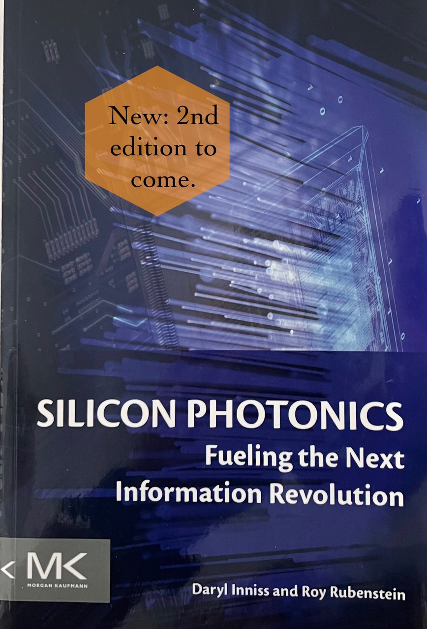
How is silicon photonics powering the AI revolution and benefitting industries from autonomous vehicles to healthcare? A new edition of the book, Silicon Photonics: Fueling the Information Revolution will reveal the answers.
A decade ago, the editor of Gazettabyte and Daryl Inniss, now Principal Market Analyst at LightCounting Market Research, wrote the book: Silicon Photonics: Fueling the Information Revolution, published by Morgan Kaufmann, part of Elsevier.
We are delighted to report that we have agreed with the publisher to proceed with a second edition.
Many of the arguments about how silicon photonics would develop, as made in the first book, have come to pass. But much has also changed, AI’s phenomenal rise and the emergence of massive AI computing clusters that work only because of photonics enabling their vast networking needs.
While AI will be the primary driver of silicon photonics in the coming years, the book will touch on emerging non-datacom/telecoms applications for silicon photonics such as Lidar and biosensors.
We look forward to our writing journey and conducting interviews with incumbents, start-ups, and academics to deepen our understanding of the technology and the market. The book will explain the technology, the emerging ecosystem, the evolving challenges in bringing silicon photonics to market, and the end applications.
One aim of the first edition was to highlight how silicon photonics would converge with the semiconductor world. Now with the advent of AI, silicon photonics is butting up to AI chips, the most complex of all compute silicon. Yet the integration of photonics and electronics is still to come. The book will discuss the chip world as well as optics.
The second edition is targeted to be published in 2027. We will provide book updates and relevant articles as we advance with our research and writing.
Daryl Inniss and Roy Rubenstein
Please feel free to leave a comment with your thoughts and suggestions regarding the second edition.

Ciena becomes a computer weaver
- Ciena is to buy optical interconnect start-up Nubis Communications for $270 million.
- The deal covers optical and copper interconnect technology for data centres
Ciena has announced its intention to buy optical engine specialist Nubis Communications for $270 million. If the network is the computer, Nubis’ optical engine and copper integrated circuit (IC) expertise will help Ciena better stitch together AI’s massive compute fabric.
Ciena signalled its intention to target the data centre earlier this year at the OFC show when it showcased its high-speed 448-gigabit serialiser-deserialiser IC technology and coherent lite modem. Now, Ciena has made a move for start-up Nubis, which plays at the core of AI data centres.
“Ciena’s expertise in high-speed components is relevant to 400G per lane Ethernet transceivers, but they never sold any products to this market,” says Vladimir Kozlov, CEO of LightCounting. “Nubis offers them an entry point with several designs and customer engagements.”
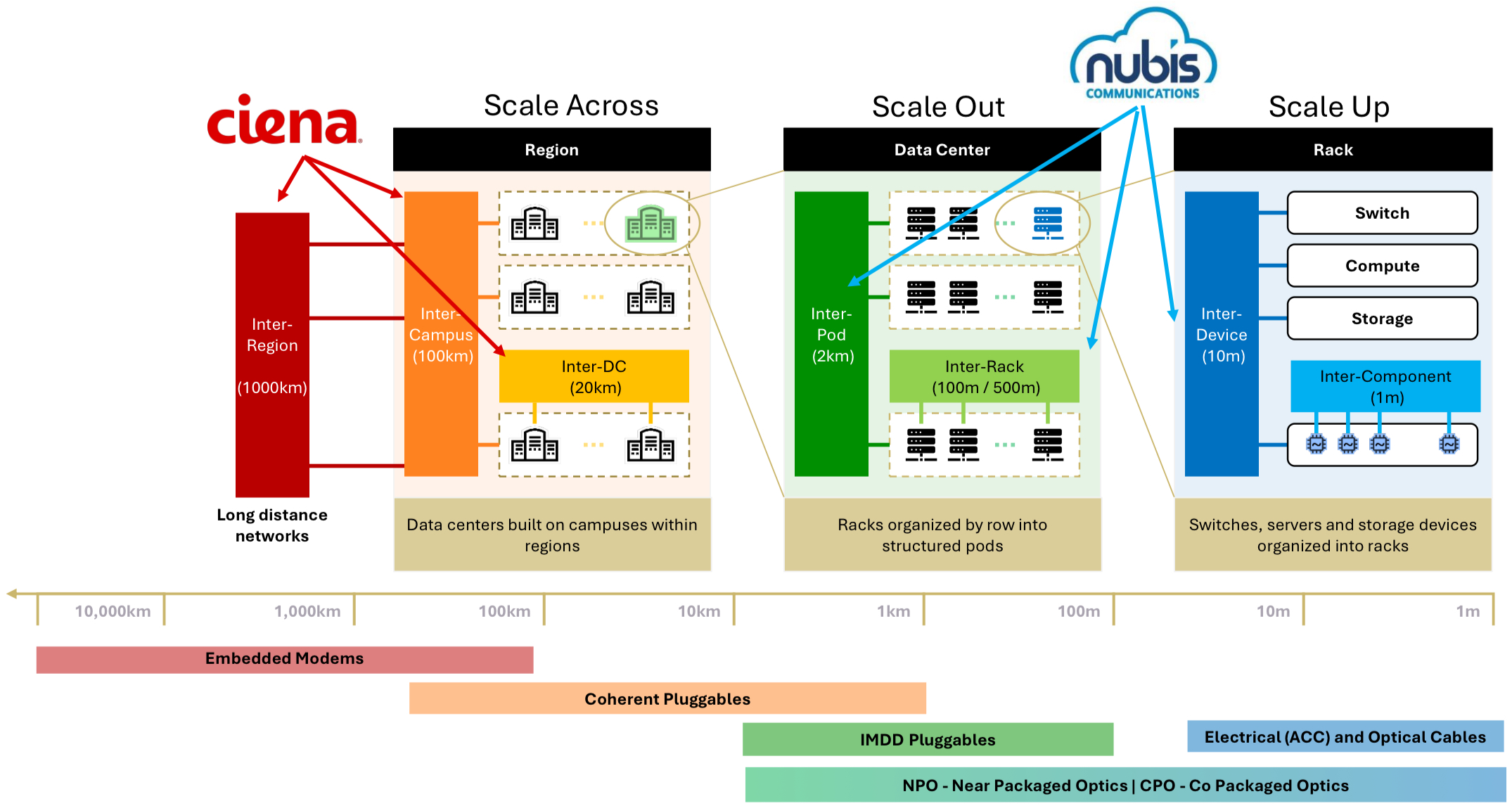
With the deal, Ciena is extending its traditional markets of wide area networks (WAN), metro, and short-reach dense wavelength division multiplexing (DWDM) to include AI networking opportunities. These opportunities include scale-across networks, where AI workloads are shared across multiple data centres, something Ciena can address, to now scale-out and scale-up networks for AI clusters in the data centre.
Puma optical engine
Nubis has developed two generations of compact optical engines for near-package optics (NPO) and co-package optics (CPO) applications. Its first-generation engine operates at 100 gigabits per second (Gbps), while its second, dubbed Puma, operates at 200 Gbps.
Nubis’s optical engine philosophy is based on escaping the optical channels from the surface of the optical engine, not its edge. The start-up also matches the number of optical channels to the electrical ones. The optical engine can be viewed as a sieve: data from the input channels flow through the chip and emerge in the same number of channels at the output. The engine acts as a two-way gateway, with one side handling electrical signals and the other, optical ones.
The Puma optical engine uses 16 channels in each direction, 16 by 200Gbps electrical signals for a total of 3.2 terabits per second (Tbps), and 16 fibres, each fibre carrying 200Gbps of data in the form of a wavelength. Puma’s total capacity is thus 6.4 terabits per second (Tbps). The engine also needs four external lasers to drive the optics, each laser feeding four channels or four fibres. The total fibre bundle of the device consists of 36 fibres: 32 for data (16 for receive and 16 for transmit), and four for the laser light sources.
Nubis is also a proponent of linear drive technology. Here, the advanced serdes on the adjacent semiconductor chip drives the optical engine, thereby avoiding the need for an on-engine digital signal processor (DSP) that requires power. The start-up has also developed a system-based simulator software tool that it uses to model the channel, from the transmitter to the receiver. The tool models not only the electrical and optical components within the channel but also the endpoints, such as the serdes.
Nitro
Nubis has an analogue IC team that designs its trans-impedance amplifiers (TIAs) and drivers used for the optical engine. The hardware compensates for channel impairments with low noise, high linearity, and at high speed. It is this channel simulator tool that Nubis used to optimise its optical engine, and to develop its second key technology, which Nubis calls Nitro —a chip that extends the reach of copper cabling.
“We use our linear optics learning and apply it to copper straight out of the gate, “said Peter Winzer, founder & CTO at Nubis, earlier this year. By using its end-to-end simulator tool, Nubis developed the Nitro IC, which extends the 1m reach of direct-attached copper to 4m using an active copper cable design. “We don’t optimise the driver chip, we optimise the end-to-end system,” says Winzer.
Nubis was also part of a novel design based on a vertical line card to shorten the trace length between an ASIC and pluggable modules.
Ciena’s gain
The acquisition of Nubis places Ciena at the heart of the electrical-optical transition inside the data centre. Ciena will cover both options: copper and optical interconnect. Ciena will gain direct-drive technology expertise for electrical and optical interfaces, enabling scale-up, as well as optical engine technology for scale-out, adding to its coherent technology expertise.

Ciena’s technologies will span coherent ultra-long-haul links all the way to AI accelerators, the heart of AI clusters. By combining Ciena’s 448-gigabit serdes with Nubis’s optical engine expertise, Ciena has a roadmap to develop 12.8Tbps and faster optical engines.
The acquisition places Ciena among new competitors that have chip and optical expertise and deliver co-packaged optics solutions alongside complex ICs such as Broadcom and Marvell.
The deal adds differentiation from Ciena’s traditional system vendor competitors, such as Cisco/ Acacia and Nokia. Huawei is active in long-haul optical and makes AI clusters. Ciena will also compete with existing high-speed optical players, including co-packaged optics specialists Ayar Labs and Ranovus, microLED player Avicena, and optical/IC fabric companies such as LightMatter and Celestial AI.
“Ciena will be a unique supplier in the co-packaged optics/near-packaged optics/active copper cabling data centre interconnect market,” says Daryl Inniss, Omdia’s thought lead of optical components and advanced fibre. “The other suppliers either have multiple products in the intra data centre market, like Broadcom and Nvidia, or they are interconnect-focused start-ups. These suppliers should all wonder what Ciena will do next inside the data centre.”
Ciena will enhance its overall expertise in chips, optics, and signal processing with the Nubis acquisition. It will also put Ciena in front of key processor players and different hyperscaler engineering teams, which drive next-generation AI systems.
Ciena will also have all the necessary parts for the various technologies, regardless of the evolving timescales associated with the copper-to-optical transition within AI systems. Ciena will add direct-detect technology and copper interconnect. On the optical side, it has coherent optical expertise, now coupled with near-package optics and co-packaged optics.
Nubis’ gain
Nubis’ 50-plus staff get a successful exit. The start-up was founded in 2020. Nubis will become a subsidiary of Ciena.
Nubis will be joining a much bigger corporate entity with deep expertise and pockets. Ciena has a good track record with its mergers. Think Nortel at the system level and Blue Planet, a software acquisition. Now the Nubis deal will bring Ciena firmly inside the data centre.
“This is a great deal for Nubis,” says Kozlov. “Congratulations to their team.”
What next?
The deal is expected to close in the fourth quarter of this year. Ciena expects the deal to start adding to its revenues from 2028, requiring Ciena and Nubis to develop products and deliver design wins in the data centre.
“Given the breadth of Ciena’s capabilities, its deep pockets, and products like its data centre out-of-band (DCOM) measurement product, router, and coherent transceivers, one can imagine that Ciena would offer more than co-packaged optics/ near-packaged optics/ active copper cabling inside the data centre,” says Inniss.

From spin-out to scale-up: OpenLight’s $34M funding
Part 1: Start-up funding
OpenLight Photonics, a Santa Barbara-based start-up specialising in silicon photonics, has raised $34 million in an oversubscribed Series A funding round.
The start-up will use the funding to expand production and its photonic integrated circuit (PIC) design staff.
OpenLight Photonics raises $34M in an oversubscribed Series A.
“We’re starting to get customers taking in production mask sets, so it’s about scaling operations and how we handle production,” says OpenLight CEO, Adam Carter (pictured). The start-up needs more PIC designers to work with customers.
Technology
OpenLight’s technology originated at Aurrion, a fabless silicon photonics start-up from the University of California, Santa Barbara.
Aurrion’s heterogeneous integration silicon photonics technology supports III-V materials, enabling components such as lasers, modulators, and optical amplification to be part of a photonic integrated circuit (PIC). Intel has its own heterogeneous integration silicon photonics process, which it has used to make millions of pluggable optical transceivers. OpenLight is offering the technology to customers effectively as a photonic ASIC design house.
Juniper Networks bought Aurrion in 2016 and, in 2022, spun out the unit that became OpenLight. Electronic design tool specialist Synopsys joined Juniper in backing the venture. Synopsys announced it was acquiring simulation company Ansys, a $35 billion deal it completed in July. Given that Synopsys would be focused on integrating Ansys, it suggested to OpenLight in January that they should part ways.
Funding
“We were only looking for $25 million to start with, and we finished at $34 million,” says Carter. Capricorn Investment Group was a late entrant and wanted to co-lead the funding round. Given initial commitments from other funders, Mayfield and Xora Innovation, set specific ownership percentages, it required an increase to accommodate Capricorn.
Xora’s first contact with OpenLight was after it approached the start-up’s stand at the OFC 2025 event held in March.
Juniper—now under HPE—is also an investor. The company played a key role in helping OpenLight while it sought funding. “Juniper could see that we were very close to an intercept point regarding our business model and our customers, so that’s why Juniper invested,” says Carter.
HPE continually looks at technologies it will require; silicon photonics with heterogeneous integration is one such technology, says Carter. However, HPE has no deal with OpenLight at this time.
Design roadmap
OpenLight is developing a 1.6-terabit PIC, now at an advanced prototype (beta) stage. The design uses eight channels for a 1.6T-DR8 OSFP pluggable design, implemented using four lasers and eight modulators, each operating at 200 gigabit-per-second (Gbps).
Carter says the first wafers will come from foundry Tower Semiconductor around October. This will be OpenLight’s largest production run — 100 wafers in four batches of 25. Some ten customers will evaluate the PICs, potentially leading to qualification.
A coarse wavelength division multiplexing (CWDM) 1.6-terabit design will follow in 2026. The CWDM uses 4 wavelengths, each at 200Gbps, on a fibre, with two such paths used for the 1.6T OSFP-XD 2xFR4 optical module.
The company is also pushing to develop 400Gbps channels, increasing the frequency response and improving the extinction ratio through process changes.
“We’ve got a whole series of experiments coming out over the next few months,“ says Carter. The frequency response of the indium phosphide modulator has already been improved by 10 gigahertz (GHz) to 90-95GHz. The process changes will be adopted for some alpha sample wafers in production that may enable modulation at 400Gbps, hence a 3.2-terabit PIC design.
“If we can show some good 3.2-terabit eyes, just as a demo, it shows that there’s a technology route to get there whenever 3.2-terabit modules are needed,” he says.
Customer growth
OpenLight’s customers have grown from three in 2023 to 17 last year to 20 actively designing. “We are growing the pipeline,” says Carter.
Early adopters were start-ups, but now larger firms are engaging Openlight. “Investors noted start-ups take more risk, but now bigger companies are coming in to drive volume,” says Carter.
Optical interconnect will drive initial volumes, but automotive and industrial sensing will follow. “The mix will change, but for the next couple of years, the revenues will be from optical interconnect,” says Carter.
Co-packaged optics is another interconnect opportunity. Here, OpenLight’s integrated laser technology would not be needed, given the co-packaged optics designs favour external laser sources. Instead, the company can offer integrated indium phosphide modulator banks or modulator banks with semiconductor optical amplifiers (SOAs), their compact size—“microns, not millimetres”—aiding packaging.
In addition to the foundry Tower Semiconductor for its wafers, OpenLight partners with Jabil, Sanmina, and TFC for the packaging and does its testing via ISC, an ASE subsidiary.
“They know test and certain customers with ISC, and ASE could do a complete turnkey solution,” says Carter. “But our priority is to get the test area set up to deal with the production; we’ve not had 100 wafers in a year being delivered for test.”
Silicon photonics
Carter, who was at Cisco when it acquired Lightwire in 2012, says silicon photonics’ potential to shrink optical designs was already recognised then. Since then, a lot of progress has been made, but now the focus is on building the supporting ecosystem. This includes a choice of foundries offering optical process design kits (PDKs) and outsourced assembly and test houses (OSATs) that can handle volumes.
Until now, silicon photonics has been all passive circuits. Now OpenLight, working with Tower and its PDK, is offering customers the ability to design and make heterogeneous integrated silicon photonics circuits. “Every customer gets the same PDK,” says Carter.
And it need not just be indium phosphide. The idea is to expand the PDK to support modulation materials such as polymer and thin-film lithium niobate. “If it is a better material, we’ll integrate it,” he says.
Having secured the funding, Carter is clear about the company’s priority: “It’s all about execution now.”
Paying homage to Harald Bock

Harald Bock, described by an optical networking executive as one of the great people of our industry, has died. Former colleagues describe the man and their sense of loss
Those who knew and worked with Harald Bock have been stunned by his sudden passing at 55. For them, Harald was a valued and much-admired friend, a deep thinker who made his views heard, quietly yet powerfully.
Last February, Harald changed jobs, becoming chief product officer at Ekinops after six years at Infinera. He was excited by the role and enjoyed his introductory period travelling to Ekinops’ sites, meeting colleagues and customers, and working on the company’s strategy.
Sylvain Quartier, Ekinops’ chief marketing & strategy officer, says it took the company a year to find the right candidate. Ekinops knew of Harald’s optical networking expertise but was impressed with his keenness to expand into what, for him, were new product areas such as routeing and cybersecurity.
“We needed someone expert in one domain and with good experience in product strategy,” says Quartier. “He was full of joy and happy to work.”
During Harald’s short spell at the company, he sharpened Ekinops’s product plans. “We’re executing his roadmap and strategy today,” says Quartier. “In six months, he had a great impact.”
Career
Harald earned his PhD in physics, specialising in polymer materials.
“Polymers may become an important material system for future high-speed [optical] modulators,” says Uwe Fischer, who was chief technology officer (CTO) at former optical networking firm, Coriant. “He was ahead of his time by doing something in his PhD thesis which is about to become important in business and technology.”
Harald’s career spanned some notable optical networking firms: Marconi, Nokia Siemens Networks, Coriant, and Infinera. He was part of Uwe Fischer’s team at Nokia Siemens Networks and Coriant. Harald’s strength was as a technologist, and had roles in several CTO offices.
Stefan Voll, then a lead product line manager and now senior director of business development at Adtran, worked with Harald at Nokia Siemens Networks in 2012.
The two were tasked with carving out the optical business of Nokia Siemens Networks in what was to become Coriant. “The carve-out was a big achievement,” says Voll. Harald represented the CTO office and Voll led the product line manager team and the two were tasked with making the product portfolio not only viable but profitable. This required aligning technical aspects with business needs, setting the foundation for Coriant’s operations.
At Coriant, Harald contributed to the development of Groove, one of the first compact modular platform for metro wavelength division multiplexing (WDM) and long-haul networks. Harald continued in the CTO office at Infinera after it acquired Coriant in 2019.
More recently, Harald served as editor of the Optical Internetworking Forum’s (OIF) 1600ZR project, taking over the role after an OIF member stepped down. The work involves standardising 1600-gigabit coherent optics for high-capacity networks. “He stepped in as smooth as possible,” says Karl Gass, optical vice chair of the OIF’s physical link layer (PLL) working group. “He knew how to manage personalities and get things done.”
Work ethic
Christian Uremovic, senior director of solution marketing at Nokia Optical Networks, worked with Harald at Coriant and Infinera. “He was a respected and valued technology guide for product line management and sales and for us in marketing,” says Uremovic. It wasn’t always an easy role; groups in the company would pull in different directions, and bringing it all together was a challenge. “Sometimes you had to make difficult decisions,” says Uremovic.
“He would like to understand basic technologies, and when, at executive meetings, he wanted to bring his opinion and convince others, he would talk quietly,” says Ekinop’s Quartier. “Everybody would be quiet because you wanted to hear him, and he made a strong impression.” With this quiet manner, Harald would progress the discussion and bring everybody in the right direction, says Quartier.
It is something Robert Richter, managing director and senior vice president, customer executive, product marketing office, at Nokia, highlights: “Harald would reiterate his view calmly, even if it annoyed some leaders, but it was always positive,” he says, adding that Harald was not the kind of guy who did what management told him. But he was always trying to change opinions constructively.
Voll reinforces this, saying Harald would not let shortcuts slide, ensuring all critical aspects were covered. “He was not afraid of conflict.” Harald would broaden discussions to bring in new angles to the point where it could be annoying. “But it was always valuable,” says Voll. “He was not fast, and that’s because he was a deep thinker. He reacted in meetings, but not immediately; he needed some time putting his thoughts together.”
Voll says Harald was focused on long-term technology trends, five to six years out, compared to product line managers’ shorter-term view. “He taught me to assess competitiveness through metrics like capacity per power consumption,” says Voll. Harald would say: “Convert it into capacity per volume or per power consumption.” Ten years ago, these were not usual metrics, but Harald used them to measure product plans. Harald would also also look product optimisations, such as whether a platform’s chips had features that were not used.
Maxim Kuschnerov, Director of R&D, at Huawei, worked with Harald at Coriant. He recalls a meeting he had with Deutsche Telekom presenting Huawei’s research topics. Afterwards, a Deutsche Telekom executive remarked that although it was framed as a research discussion, Kuschnerov kept steering the conversation toward commercial applications and customer value: “It reminds me of a guy at Coriant who talks about use cases a lot — Harald Bock”. Smiling, Kuschnerov replied: “Where do you think I was taught to think like that? I worked with Harald!”
Traits
Ekinops’ Quartier highlights Harald’s general cheerfulness: “He was always smiling, which was much appreciated.”
Richter, who worked with Harald for 18 years at Nokia Siemens Networks and Coriant, describes him as the most empathetic person he has met. “He was always listening to people and was very patient,” he says. Harald would bring cakes to the office from vacations and would never speak ill of others. He’d keep positive even during challenging times and in that sense, he was a role model, says Richter: “It was always a pleasure to talk to him over a coffee. He was open to a dialogue.”
Harald had an impressive fitness routine. “He’d bike 20km, swim for an hour, then come to the office relaxed,” says Voll. Until recently, Fischer and Harald would go biking on 40-kilometre rides. “Sometimes he was behind in my slipstream, then we change positions,” says Fischer. “We were proud of the competitive speed and times we could achieve together.” He was a keen water polo player in his youth.

Fluent in English, French, and his native German, Harald read books in all three languages. He adored France – his wife is French – with its pastries and Brittany with its Hydrangeas. He said how the Hydrangeas in his garden struggled, yet on seeing the flourishing bands of colour in Brittany (pictured), he was determined to try again.
Legacy
When colleagues talk about Harald, they recount his warmth and character.
Uremovic recollects sharing an office and hearing Harald’s diplomatic charm on calls. These experiences have shaped his ability to connect better with others. He will also miss their talks: “To me, he was like a big brother.”
Harald made a deep impression during his short time at Ekinops. “We miss him,” says Quartier. “We will always have his memory at Ekinops.”
Fischer highlights their shared interests in life – sport and a love of France.”There was a lot of mutual understanding which we didn’t need to put into words,” says Fischer. “Sometimes, when you feel close to somebody, you don’t even need to talk.”
Fischer, who has watched Harald’s career over the years, laments a life cut short. “He was at the peak of his career,” he says. ”He brought to Ekinops all his experience of the last 20 to 30 years so this period was maybe the most impactful time of his life.”
Richter’s grief over his lost colleague is evident in his sombre tone and demeanour, perhaps the deepest tribute one can pay to someone held so dear.
IOWN’s all-photonic network vision
What is the best way to send large amounts of data between locations? Its a question made all the more relevant with the advent of AI, and one that has been preoccupying the Innovative Optical and Wireless Network (IOWN) Global Forum that now has over 160 member companies and organisations
Optical networking has long established itself as the high-speed communications technology of choice for linking data centres or large enterprises’ sites.
The IOWN Global Forum aims to take optical networking a step further by enabling an all-optical network, to reduce the energy consumption and latency of communication links. Latency refers to the time it takes transmitted data to start arriving at the receiver site.
“The IOWN all-photonic network is the infrastructure for future enterprise networking,” says Masahisa Kawashima, IOWN technology director, IOWN development office, NTT Technology working group chair, IOWN Global Forum.
“The main significance of IOWN is setting a roadmap,” says Jimmy Yu, vice president and optical transport senior analyst at Dell’Oro. “It helps component and systems companies understand what technology and architectures that companies, such as NTT, are interested in for a next-generation optical and wireless network. It also fosters industry collaboration.”
IOWN architecture
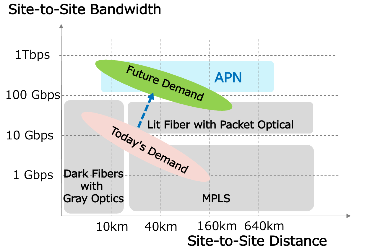
The IOWN Global Forum’s all-optical network (APN) is to enable optical connectivity from edge devices to data centres at speeds exceeding 100 gigabits-per-second (Gbps).
The Forum envisions energy and latency performance improvements by driving optics to the endpoints. Linking endpoints will require a staged adoption of photonic technology as it continues to mature.
Professor Ioannis Tomkos, a member of the Optical Communications Systems & Networks (OCSN) Research Lab/Group at the Electrical and Computer Engineering Department at the University of Patras, says the aim of the IOWN Global Forum is to gradually replace electronics-based transmission, switching, and even signal processing functions with photonics. The OCSN Group recently joined the IOWN Global Forum.
The Forum has defined a disaggregated design for the all-photonic network. The following stages will include using optics to replace copper interconnect within platforms, interfacing photonics to chips, and, ultimately, photonic communications within a chip.
“If information-carrying light signals can remain in the optical domain and avoid opto-electronic and electro-optical conversions, that will ensure enhanced bandwidth and much reduced power consumption per bit,” says Tomkos.
The IOWN Global Forum was created in 2019 by Japanese service provider, NTT, Sony, and Intel. Since then, it has grown to over 160 members, including cloud players Google, Microsoft, and Oracle, telecom service providers British Telecom, Orange, KDDI, Telefónica, and companies such as Nvidia.
The Forum has developed an IOWN framework that includes the all-photonic network, digital twin computing (DTC), and a ‘cognitive foundation’ (CF). Digital twin computing enables the creation of virtual representations of physical systems, while the cognitive foundation is the architecture’s brain, allocating networking and computing resources as required.
“We expect future societies will be more data-driven and there will be many applications that collect huge real-time sensor data and analyse them,” says Kawashima. “The IOWN all-photonic network and disaggregated computing platforms will enable us to deploy digital twin application systems in an energy-efficient way.”
Optical infrastructure
The IOWN Global Forum’s all-photonic network uses open standards, such as the OpenROADM (Open reconfigurable optical add-drop multiplexing) Multi-Source Agreement (MSA), the OIF and the OpenZR+ MSA pluggable coherent optics, and the OpenXR Optics Forum standards. The IOWN Global Forum also adheres to the ‘white box’ platform designs defined by the Telecom Infra Project (TIP).
“There is a lot of similarity with the approach and objectives of TIP,” says an unnamed industry veteran who has observed the IOWN Global Forum’s organisation since its start but whose current employer is not a member. “Although the scope is not the same, I cannot help but wonder why we don’t combine the two as an industry.”
Kawashima says that optical hardware, such as ROADMs, pluggable optics, and transponder boards, is located at one site and operated by one organisation. Now, the Forum has disaggregated the design to enable the ROADM and transponders to be in different locations: the transponder can be deployed at a customer’s premises, remote from the ROADM’s location.
“We allow the operator of the switch node to be different from the operator of the aggregator node, and we allow the operator of the transponder node to be different from the operator of the ROADM nodes,” says Kawashima.
The disaggregation goal is to encourage the growth of a multi-operator ecosystem, unlike how optical transport is currently implemented. It is also the first stage in making the infrastructure nodes all-optical. Separating the transponder and the ROADMs promises to reduce capital expenditure, as the transceiver nodes can be upgraded separately from the ROADMs that can be left unchanged for longer.
Kawashima says that reducing infrastructure capital expenditure promises reduced connectivity prices: “Bandwidth costs will be cheaper.”
Service providers can manage the remote transponders at the customers’ sites, creating a new business model for them.
Early use cases
IOWN has developed several use cases as it develops the technology.
One is a data centre interconnect for financial service institutions that conduct high-frequency trading across geographically dispersed sites.
Another is remote video production for the broadcast industry. Here, the broadcast industry would use an all-photonic network to connect the site where the video feed originates to the cloud, where the video production work is undertaken.
A third use case is for AI infrastructure. An enterprise would use the all-photonic network to link its AI product development engineers to GPU resources hosted in the cloud.
If the network is fast enough and has sufficiently low latency, the GPUs can source data from the site, store it in their memory, process it, and return the answer. The aim is for enterprises not to need to upload and store their data in the cloud. “So that customers do not have to be worried about data leakages,” says Kawashima.
The Forum also publishes documents. “Once the proof-of-concept is completed, that means that our solution is technically proven and is ready for delivery,” says Kawashima.
Goals
At OFC 2025, held earlier this year, NTT, NTTCom, Orange, and Telefónica showcased a one terabit-per-second optical wavelength circuit using the IOWN all-photonics network.

The demonstration featured a digital twin of the optical network, enabling automated configuration of high-speed optical wavelength circuits. The trial showcased the remote control of data centre communication devices using an optical supervisory channel.
The Forum wants to prove the technical feasibility of the infrastructure architecture by year-end. It looks to approve the remote GPUs and financial services use cases.
“What we are trying to achieve this year is that the all-photonic network is commercially operable, as are several use cases in the enterprise networking domain,” says Kawashima.
IOWN’s ultimate success will hinge on the all-photonic network’s adoption and economic viability. For Kawashima, the key to the system architecture is to bring significant optical performance advantages.
Tomkos cautions that this transformation will not happen overnight and not without the support of the global industry and academic community. But the promise is growth in the global network’s throughput and reduced latency in a cost and power-efficient way.

Glenn Wellbrock’s engineering roots
After four decades shaping optical networking, Glenn Wellbrock has retired. He shares his career highlights, industry insights, and his plans to embrace a quieter life of farming and hands-on projects in rural Kansas.
Glenn Wellbrock’s (pictured) fascination with telecommunications began at an early age. “I didn’t understand how it worked, and I wanted to know,” he recalls.
Wellbrock’s uncle had a small, rural telephone company where he worked while studying, setting the stage for his first full-time job at telecom operator, MCI. Wellbrock entered a world of microwave and satellite systems; MCI was originally named Microwave Communications Incorporated. “They were all ex-military guys, and I’m the rookie coming out of school trying to do my best and learn,” says Wellbrock.
The challenge that dominated the first decade of this century.
The arrival of fibre optics in the late 1980s marked a pivotal shift. As colleagues hesitated to embrace the new “glass” technology, Wellbrock seized the opportunity. “I became the fibre guy,” he says. “My boss said, ‘Anything breaks over there, it’s your problem. You go fix it.’”
This hands-on role propelled him into the early days of optical networking, where he worked on asynchronous systems with bit rates ranging from hundreds of kilobits to over a megabit, before SONET/SDH standards took over.
By the 1990s, with a young family, Wellbrock moved to Texas, contributing to MCI’s development of OC-48 (2.5 gigabit-per-second or Gbps) systems, a precursor to the high-capacity networks that would define his career.
Hitting a speed wall
One of Wellbrock’s proudest achievements was overcoming the barrier to get to speeds faster than 10Gbps, a challenge that dominated the first decade of this century.
Polarisation mode dispersion (PMD) in an optical fibre was a significant hurdle, limiting the distance and reliability of high-speed links. By then, he was working at a start-up and did not doubt that using phase modulation was the answer.
Wellbrock recalls conversations he had with venture capitalists at the time: “I said: ‘Okay, I get we are a company of 40 guys and I don’t even know if they can build it, but somebody’s going to do it, and they’re going to own this place.’”
Wellbrock admits he didn’t know the answer would be coherent optics, but he knew intensity modulation direct detection had reached its limits.
For a short period, Wellbrock was part of Marconi before joining Verizon in 2006. In 2007, he was involved in a Verizon field trial between Miami and Tampa, 300 miles apart, which demonstrated a 100Gbps direct-detection system. “It was so manual,” he admits. “It took three of us working through the night to keep it working so we could show it to the executives in the morning.”
While the trial passed video, it was clear that direct detection wouldn’t scale. The solution lay in coherent detection, which Wellbrock’s team, working with Nortel (acquired by Ciena), finally brought to market by 2009.
“Coherent was like seeing a door,” he says. “PMD was killing you, but you open the door, and it’s a vast room. We had breathing room for almost two decades.”
Verizon’s lab in Texas had multiple strands of production fibre that looped back to the lab every 80km. “We could use real-world glass with all the impairments, but keep equipment in one location,” says Wellbrock.
This setup enabled rigorous testing and led to numerous post-deadline papers at OFC, cementing Verizon’s reputation for optical networking innovation.
Rise of the hyperscalers
Wellbrock’s career spanned a transformative era in telecom, from telco-driven innovation to the rise of hyperscalers like Google and Microsoft.
He acknowledges the hyperscalers’ influence as inevitable due to their scale. “If you buy a million devices, you’re going to get attention,” he says. “We’re buying 100 of the same thing.”
Hyperscalers’ massive orders for pluggable modules and tunable lasers—technologies telcos like Verizon helped pioneer—have driven costs down, benefiting the industry.
However, Wellbrock notes that telcos remain vital for universal connectivity. “Every person, every device is connected,” he says. “Telcos aren’t going anywhere.”
Reliability remains a core challenge, particularly as networks grow. Wellbrock emphasises dual homing—redundant network paths—as telecom’s time-tested solution. “You can’t have zero failures,” he says. “Everything’s got a failure rate associated with it.”
He sees hyperscalers grappling with similar issues, as evidenced by a Google keynote at the Executive Forum at OFC 2025, which sought solutions for network failures linking thousands of AI accelerators in a data centre.
Wellbrock’s approach to such challenges is rooted in collaboration. “You’ve got to work with the ecosystem,” he insists. “Nobody solves every problem alone.”
Hollow-core fibre
Looking forward, what excites Wellbrock is hollow-core fibre, which he believes could be as transformative as SONET, optical amplifiers, and coherent detection.
Unlike traditional fibre, hollow-core fibre uses air-filled waveguides, offering near-zero loss, low latency, and vast bandwidth potential. “If we could get hollow-core fibre with near-zero loss and as much bandwidth as you needed, it would give us another ride at 20 years’ worth of growth,” he says. “It’s like opening another door.”
While companies like Microsoft are experimenting with hollow-core fibre, Wellbrock cautions that widespread adoption is years away. “They’re probably putting in [a high fibre glass] 864 [strand]-count standard glass and a few hollow core [strands],” he notes.
For long-haul routes, the technology promises lower latency and freedom from nonlinear effects, but challenges remain in developing compatible transmitters, receivers, and amplifiers. “All we’ve got to do is build those,” he says, laughing, acknowledging the complexity.
Wellbrock also highlights fibre sensing as a practical innovation, enabling real-time detection of cable damage. “If we can detect an excavator getting closer, we can stop it before it breaks a fibre link,” he explains. This technology, developed in collaboration with partners like NEC and Ciena, integrates optical time-domain reflectometry (OTDR) into transmission systems, thereby enhancing network reliability.
Learnings
Wellbrock’s approach to innovation centres on clearly defining problems to engage the broader ecosystem. “Defining the problem is two-thirds of solving it,” he says, crediting a Verizon colleague, Tiejun J. Xia, for the insight. “If you articulate it well, lots of smart people can help you fix it.”
This philosophy drove his success at OFC, where he used the conference to share challenges, such as fibre sensing, and rally vendor support. “You’ve got to explain the value of solving it,” he adds. “Then you’ll get 10 companies and 1,000 engineers working on it.”
He advises against preconceived solutions or excluding potential partners. “Never say never,” he says. “Be open to ideas and work with anybody willing to address the problem.”
This collaborative mindset, paired with a willingness to explore multiple solutions, defined his work with Xia, a PhD associate fellow at Verizon. “Our favourite Friday afternoon was picking the next thing to explore,” he recalls. “We’d write down 10 possible things and pull on the string that had legs.”

Fibre to Farming
As Wellbrock steps into retirement, he is teaming up with his brother.
The two own 400 acres in Kansas, where wheat farming, hunting, and fishing will define their days. “I won’t miss 100 emails a day or meetings all day long,” he admits. “But I’ll miss the interaction and building stuff.”
Farming offers a chance to work with one’s hands, doing welding and creating things from metal. “I love to build things,” he says. “It’s fun to go, ‘Why hasn’t somebody built this before?’
Farming projects can be completed in a day or over a weekend. “Networks take a long time to build,” he notes. “I’m looking forward to starting a project and finishing it quickly.”
He plans to cultivate half their land to fund their hobbies, using “old equipment” that requires hands-on maintenance—a nod to his engineering roots.
OFC farewell
Wellbrock retired just before the OFC show in March 2025. His attendance was less about work and more about transition, where he spent the conference introducing his successor to vendors and industry peers, ensuring a smooth handoff.
“I didn’t work as hard as I normally do at OFC,” he says. “It’s about meeting with vendors, doing a proper handoff, and saying goodbye to folks, especially international ones.” He also took part in this year’s OFC Rump Session.
Wellbrock admits to some sadness. Yet, he remains optimistic about his future, with plans to possibly return to OFC as a visitor. “Maybe I’ll come just to visit with people,” he muses.
Timeline
- 1984: MCI
- 1987: Started working on fibre
- 2000: Joined start-ups and, for a short period, was part of Marconi
- 2004: Joined Worldcom, which had bought MCI
- 2006: Joined Verizon
- 2025: Retired from Verizon
A tribute
Prof. Andrew Lord, Senior Manager, optical and quantum research, BT
I have had the privilege of knowing Glenn since the 1990s, when BT had a temporary alliance with MCI. We shared a vendor trip to Japan, where I first learnt of his appetite for breakfasting at McDonald’s!
Glenn has been a pivotal figure in our industry since then. A highlight would be the series of ambitious Requests For Information (RFIs) issued by Verizon, which would send vendor account managers scurrying to their R&D departments for cover.
Another highlight would be the annual world-breaking Post-Deadline Paper results at OFC: those thrilling sessions won’t be the same without a Wellbrock paper and neither will the OFC rump sessions, which have benefited from his often brutal pragmatism, always delivered with grace (which somehow made it even worse when defeating me in an argument!).
But it’s grace that defines the man who always has time for people and is always generous enough to share his views and experiences. Glenn will be sorely missed, but he deserves a fulfilling and happy retirement.
OFC 2025: reflecting on the busiest optics show in years
The discussion covers the hot topics of the show and where the industry is headed next. Click here.
OFC: After the aliens, a decade to rewire the Earth
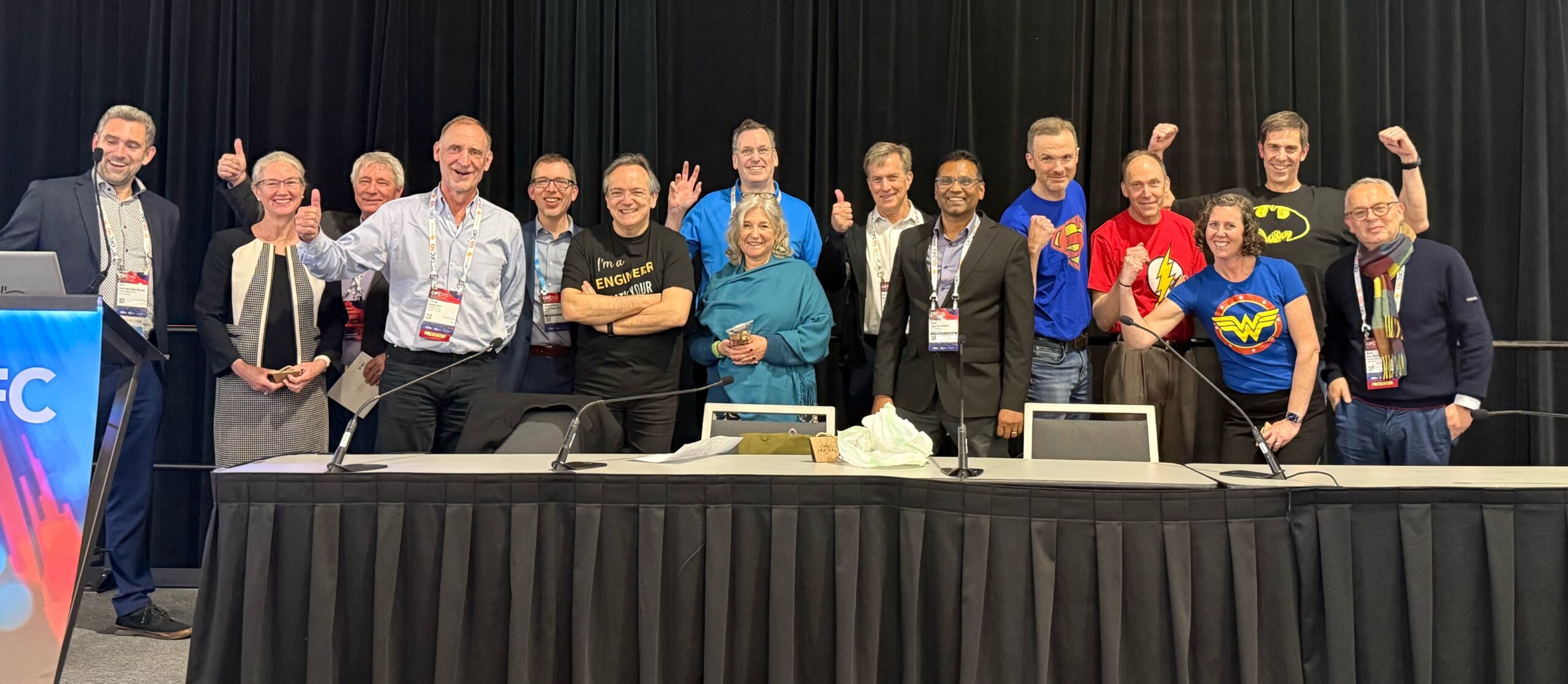
At the OFC 2025 Rump Session, held in San Francisco, three teams were set a weighty challenge. If a catastrophic event—a visit by aliens —caused the destruction of the global telecommunications network, how would each team’s ‘superheroes’ go about designing the replacement network? What technologies would they use? And what issues must be considered?
The Rump Session tackled a provocative thought experiment. If the Earth’s entire communication infrastructure vanished overnight, how would the teams go about rebuilding it?
Twelve experts – eleven from industry and one academic – were split into three teams.
The teams were given ten years to build their vision network. A decade was chosen as it is a pragmatic timescale and would allow the teams to consider using emerging technologies.
The Rump Session had four rounds, greater detail being added after each.
The first round outlined the teams’ high-level visions, followed by a round of architectures. Then a segment detailed technology, the round where the differences in the team’s proposals were most evident. The final round (Round 4), each team gave a closing statement before the audience chose the winning proposal.
The Rump Session mixed deep thinking with levity and was enjoyed by the participants and audience alike.
Round 1: Network vision
The session began with each team highlighting their network replacement vision.
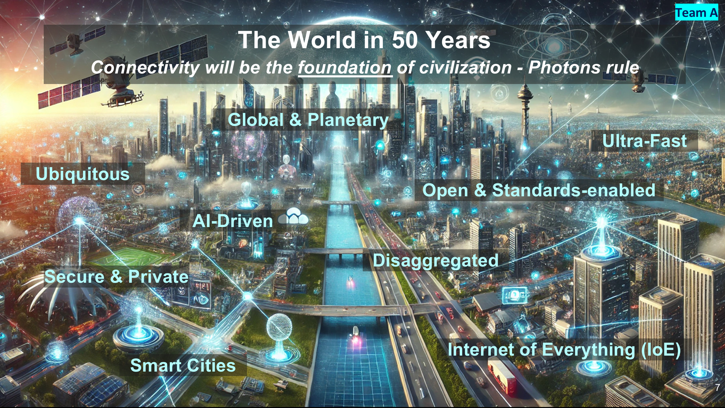
Team A’s Rebecca Schaevitz opened by looking across a hundred-year window. Looking back fifty years to 1975, networking and computing were all electrical, she said, telephone lines, mainframe computing, radio and satellite.
Schaevitz said that by 2075, fifty years hence, connectivity will be the foundation of civilisation. The key difference between the networks a century apart is the marked transition from electrons to photons.
In the future vision, everything will be connected—clothes, homes, roads, even human brains—using sensors and added intelligence. As for work, offices will be replaced with real-time interactive holograms (suggesting humanity will still be working in 2075).
Schaevitz then outlined what must be done in the coming decade to enable Team A’s Network 2075 vision.
The network’s backbone must be optical, supporting multiple wavelengths and quantum communications. Team A will complement the fixed infrastructure with terabit-speed wireless and satellite mega-constellations. And AI will enable the network to be self-healing and adaptive, ensuring no downtime.
Vijay Vusirikala outlined Team B’s network assumptions. Any new network will need to support the explosive growth in computing and communications while being energy constrained. “We must reinvent communications from the ground up for maximum energy savings,” said Visurikala.
But scarcity—in this case energy—spurs creativity. The goal is to achieve 1000x more capacity for the same energy demand.
The network will have distributed computing based on mega data centres and edge client computing. Massive bandwidth will be made available to link humans and to link machines. Lastly, just enough standardisation will be used for streamlined networking.
Team C’s Katharine Schmidtke closed the network vision round. The goal is universal and cheap communications, with lots of fibre deployed to achieve this.
The emphasis will be on creating a unified fixed-mobile network to aid quick deployment and a unified fibre-radio spectrum for ample connectivity.
Team C stressed the importance of getting the network up and running by using a modular network node. It also argued for micro data centres to deliver computing close to end users.
Global funding will be needed for the infrastructure rebuild, and unlimited rights of way will be a must. Unconstrained equipment and labour will be used at all layers of the network.
Team C will also define the communication network using one infrastructure standard for interoperability. One audience member questioned the wisdom of a tiny committee alone specifying such a grand global project.
The network will also be sustainable by recycling the heat from data centres for crop production and supporting local communities.
Round 2: Architectures
Team A’s Tad Hofmeister opened Round 2 by saying what must change: the era of copper will end – no copper landlines will be installed. The network will also only use packet switching, no more circuit switch technology. And IPv4 will be retired (to great cheering from the audience).
Team A also proposed a staged deployment. First, a network of airborne balloons will communicate with smartphones and laptops, which will be connected to the ground using free-space optical links.
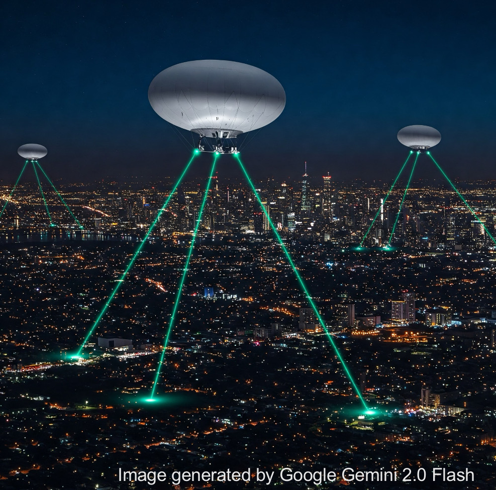
Stage 2 will add base stations complemented with satellite communications. Fibre will be deployed on a massive scale along roads, railways, and public infrastructure.
Hofmeister stressed the idea of the network being open and disaggregated with resiliency and security integral to the design.
There will be no single mega-telecom or hyperscaler; instead, multiple networks and providers will be encouraged. To ensure interoperability, the standards will be universal.
Security will be based on a user’s DNA key. What about twins? asked an audience member. Hofmeister had that covered: time-of-birth data will be included.
Professor Polina Bayvel detailed Team B’s architectural design. Here, packet and circuit switching is proposed to minimise energy/bit/ km. It will be a network with super high bandwidths, including spokes of capacity extending from massive data centres connecting population centres.

Bayvel argued the case for underwater data centres: 15 per cent of the population live near the coast, she said, and an upside would be that people could work from the beach.
Team C’s Glenn Wellbrock proposed unleashing as much bandwidth as possible by freeing up the radio spectrum and laying hollow-core fibre to offer as much capacity as possible.
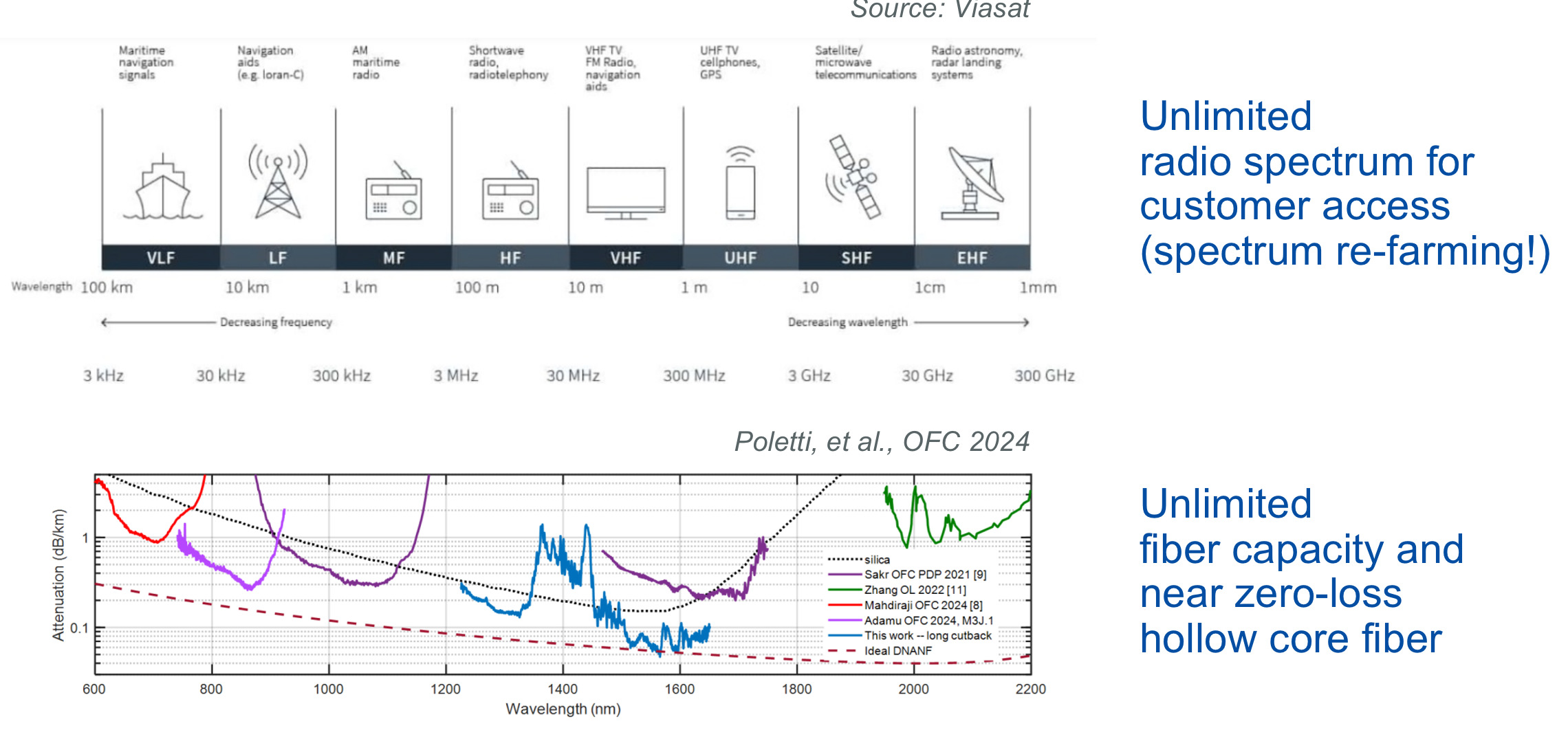
Wellbrock views hollow-core fibre as a key optical communications technology that promises years of development, just like first erbium-doped fibre amplifiers (EDFAs) and then coherent optics technology have done.
Team C showed a hierarchical networking diagram mapped onto the geography of the US – similar to today’s network – with 10s of nodes for the wide area network, 100s of metropolitan networks, and 10,000s of access nodes.
Wellbrock proposes self-container edge nodes based on standardised hardware to deliver high-speed wireless (using the freed-up radio spectrum) and fibre access. There would also be shared communal hardware, though service providers could add their own infrastructure. Differentiation would be based on services.
AI would provide the brains for network operations, with expert staff providing the initial training.
Round 3: Technologies
Round 3, the enabling technologies for the new network, revealed the teams’ deeper thinking.
Team A’s Chris Doerr advocated streamlining and pragmatism to ensure rapid deployment. Silicon photonics will make a quick, massive-scale, and economic deployment of optics possible. Doerr also favours massive parallelism based on 200 gigabaud on-off keying (not PAM-4 signalling). With co-packaged optics added to chips, such parallel optical input-output and symbol rate will save significant power.
Standards for all aspects of networking will be designed first. Direct detection will be used inside the data centre; coherent digital signal processing will be used everywhere else. More radically, in the first five years, all generated intellectual property regarding series, converters, modems, and switch silicon will be made available to all competition. Chips will be assembled using chiplets.
For line systems, C-band only followed by the deployment of Vibranium-doped optical amplifiers (Grok 3 gives a convincing list of the hypothetical benefits of VDFAs). Parallelism will also play a role here, with spatial division multiplexing preferred to combining a fibre’s O, S, C and L bands.
Like Team C, Doerr also wants vast amounts of hollow-core fibre. It may cost more, but the benefits will be long-term, he said.
Peter Winzer (Team B) also argued for parallelism and a rethink in optics: the best ‘optical’ network may not be ‘optical’ given that photons get more expensive the higher the carrier frequency. So, inside the data centre, using the terahertz band and guided-wave wire promises 100x energy per bit benefits compared to using O-band or C-band optics.
Winzer also argues for 1000x more energy-efficient backbone connectivity by moving to 10-micron wavelengths and ultra-wideband operation to compensate for the 10x spectral efficiency loss that results. But for this to work, lots of fibre will be needed. Here, hollow-core fibre is a possible option.
Chris Cole brought the round to a close with radical ways to get the networking deployed. He mentioned Meta’s Bombyx, an installation machine that spins compact fibre cables along power lines.
Underground cabling would use nuclear fibre boring (including the patent number) which produces so much heat that it bores a tunnel while lining its walls with the molten material it produces. An egg-shaped portable nuclear reactor to power data centre containers was also proposed.
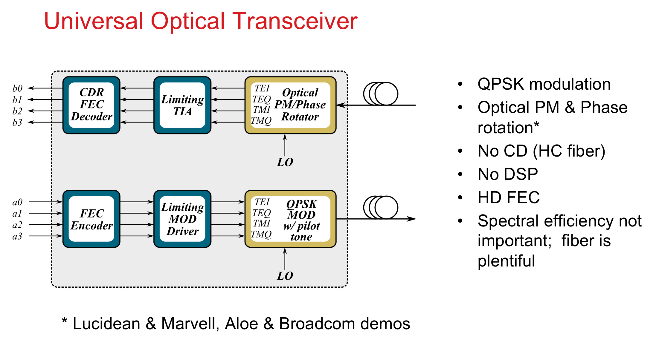
Cole defined a ‘universal’ transceiver with quadruple phase-shift keying (QPSK) modulation with no digital signal processing. “Spectral efficiency is not important as fibre will be plentiful,” says Cole.
Completing arguments
After each team had spent a total of some 14 minutes outlining their networks, they were given one more round for final statements.
Maxim Kuschnerov expanded on the team’s first-round slide, which outlined the ingredients needed to enable its Network 2075 vision. He also argued that every network element and connected device should be part of a global AI network. And AI will help co-design the new access network.
The new network will enable a massive wave of intelligent devices. Data will be kept at the edge, and the network will enable low-latency communications and inferencing at the edge.
Team B’s Dave Welch outlined some key statements: fusion energy will power the data centres with 80 per cent of the energy recycled from the heat. Transistors will pass the 10THz barrier, there will be 1000x scaling for the same energy, and an era of atto-joules/bit will begin. “And human-to-human interactions will still make the world go round,” says Welch.
Team C’s Jörg-Peter Elbers ended the evening presentations by outlining schemes to enable the new network: high-altitude platforms in a mega constellation (20km up) trailing fibre to the ground.
Such fibres and free-space links would also act as a sensing early-warning system in case the aliens returned.

Lastly, Elbers suggested we all get a towel (an important multi-purpose tool as outlined in Douglas Adams’ The Hitchhiker’s Guide to the Galaxy). A towel can be used for hand-to-hand combat (when wet), ward off noxious fumes, and help avoid the gaze of the Ravenous Bugblatter beast of Traal. Lastly, and in the spirit of the evening, if all else fails, a towel can be used for sending line-of-sight, low-bandwidth smoke signals.
Team C ended the presentations by throwing towels into the audience, like tennis stars after a match.

Common threads
All the teams agreed that fibre was necessary for the network backbone, with hollow-core fibre widely touted.
Two of the teams emphasised a staged rollout and all outlined ways to avoid the ills of existing legacy networks.
Differences included using satellites rather than fibre-fed high-altitude balloons, which are quicker and cheaper to deploy, and the idea of container edges rather than a more centralised service edge. All the teams were creative with their technological approaches.
What wasn’t discussed – it wasn’t in the remit – was the impact of a global disconnect on the world’s population. We would suddenly become broadband have-nots for several years, disconnected from smartphones and hours-per-day screen time.
The teams’ logical assumption was to get the network up and running with even greater bandwidth in the future. But would gaining online access after years offline change our habits? Would we be much more precious in using our upload and download bits? And what impact would a global comms disconnect have on society? Would we become more sociable? Would letter-writing become popular again? And would local communities be strengthened?
Maxim Kuschnerov came closest to this when, in his summary talk, he spoke about how the following iteration of network and communications should be designed to be a force for good for humanity and for its economic prospects.
Team winners
The audience chose Team B’s network proposal. However, the choice was controversial.
An online voting scheme, which would have allowed users to vote and change their vote as the session progressed, worked perfectly, but keeled over on the night.
The organisers’ fallback plan, measuring the decibel level of the audience’s cheers for each team, ended in controversy.
First, not all the Session attendees were present at the end. Second, a couple of the participants were seen self-cheering into a microphone. Evidence, if needed, as to the seriousness the ‘superheroes’ embraced architecting a new global network.
“It has been an evening of pure creative chaos: the more time I spend reflecting on the generated ideas, the more their value increases to me,” says Antonio Tartaglia of Ericsson, one of the organisers. “The voting chaos has been an act of God, because all three teams deserved to win.”
Tartaglia came up with this year’s theme for the Rump Session.
“Rump sessions are all about creative debate, and this year’s event took that to its full potential,” says Dirk van den Borne of Juniper Networks, another of the organisers. “Micro data centres, fibre-tethered balloons, Terahertz waveguides, and communication by pigeon; the sheer breath of ideas shows what an exciting and inventive industry we’re working in.”
The evening ended with a tribute to Team C’s Glenn Wellbrock. BT’s Professor Andrew Lord acknowledged Wellbrock’s career and contribution to optical communications.
Wellbrock officially retired days before the Rump Session.