
Silicon photonics grapples with 3D packaging demands
Hesham Taha (pictured), CEO of start-up Teramount, is more upbeat about silicon photonics than ever. But, as he outlines, challenges remain.
Hesham Taha is putting in the miles. The CEO of Teramount has been travelling to the East and West to meet with companies.
Termount is working closely with customers and partners adopting its technology that adds fibre to silicon photonics chips.
“We’re shipping units to customers and partners, and we need to be close to them as they integrate our components and address the challenges of integration,” says Taha.
Teramount
For Taha, connecting fibre to a silicon photonics chip inside a pluggable optical transceiver is relatively straightforward.
Far more challenging is when the optical engine and chip are packaged together, known as co-packaged optics. Such a tight coupling raises reliability challenges.
The optical engine is close to the large, heat-generating chip, introducing manufacturing and reliability issues. Also, the fibre-connect to the optical engine inside the package must be scalable. Scaling is key because with each chip generation – whether an AI accelerator or a switch chip – the input-output (I/O) requirements grow.
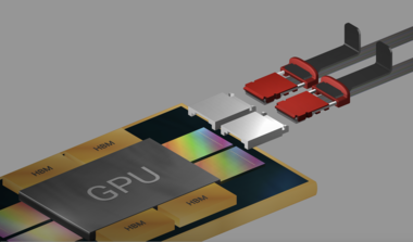
Teramount’s technology couples the fibre to the silicon photonics chip using a photonic plug and photonic bump.
The photonic plug holds the fibres and couples them to the silicon photonics chip via a photonic bump, a component made during the silicon photonics wafer’s processing.
The photonic bump has two elements: a wideband deflector and a lens mirror for beam expansion. Expanding the light beam enables larger assembly tolerances.
The resulting wafer-level manufacturing may be more complicated, says Taha, but the benefits include relaxed tolerances in the assembly, wideband surface coupling, and the testing of the wafer and the die.
The photonic bump-and-plug combination also enables detachable optics for co-packaged optics designs, benefitting their manufacturing. (For more about Teramount’s technology, click here)
Silicon Photonics meets semiconductor thinking
Taha sees silicon photonics as a platform that enables the integration of optical functions at the wafer scale using standard semiconductor manufacturing techniques.
“It [silicon photonics design] has the same way of thinking as semiconductor people: chip designers, foundries, and packaging people,” says Taha. The result is that silicon photonics is bringing optics to chip design.
The growing maturity of the technology, and the emergence of foundries such as TSMC, GlobalFoundries, Tower Semiconductor, Intel, and ST Microelectronics offering silicon photonics, means that companies with photonic designs can be fabless; a model that has benefitted the chip industry.
Photonic chip designers can use a large foundry’s process design kit (PDK) and send off their silicon photonics designs to be manufactured in volume.
As for co-packaged optics, Taha sees it as a key in the evolution of silicon photonics. Co-package optics is the realisation of silicon photonics whereby optics is integrated next to advanced semiconductor chips.
Industry developments
The growing interest in silicon photonic and co-packaged optics is also evident in some recent announcements, driven by the AI compute scaling needs.
ST Microelectronics unveiled its 300mm wafer PIC100 silicon photonics technology. ST Microelectronics was active in silicon photonics 10 years ago and has returned due to the AI opportunity.
Marvell announced it offers a co-packaged optics solution for accelerator chips to address scale-up networking for AI architectures.
Leading foundry TSMC has outlined its silicon photonics roadmap, which includes co-packaged optics.
And at the GTC 2025 AI developers conference, Nvidia announced it is adding co-packaged optics to its switch platforms for scale-out networking.
“All this is not a surprise because this is where we expected silicon photonics to be one day when we founded the company 10 years ago,” says Taha. “It is just that this day is happening now.”
Teramount sees its fibre attach product as a part of an emerging ecosystem to enable standard semiconductor high-volume manufacturing.
This ecosystem comprises chip designers, foundries, OSATs [outsourced semiconductor assembly and test service providers], and system integrators.
But there are challenges. There may be wafer-scale manufacturing, but issues remain on the integration-packaging side.
“This is why we need to travel, to align with the different partners,” says Taha.
Challenges
Teramount is seeing challenges first-hand given its fibre-attach vantage point. Taha also highlights commercial issues still to be resolved.
The technical challenges revolve around integrating the silicon photonics die with the accompanying lasers and fibres in an advanced package.
Unlike a traditional pluggable optical transceiver, the silicon photonics chip is inserted in a hot environment and must meet operational temperatures of 85oC and even 105oC.
Multiple reflow soldering steps during manufacturing expose the packaging to even higher temperatures (270oC) and thermal stresses.
“These are new technical challenges that silicon photonic chip integration must meet 3D packaging requirements,” says Taha.
3D packaging has requirements that affect the fibre attach. For example, the silicon photonics chip is thinner than the die used in a pluggable if through-silicon via (TSV) technology is used.
TSV refers to the way a vertical electrical connector is done that passes through the die. Any mechanical stresses or warpage impacts the resulting optical performance of the die.
“Co-package optics is creating new challenges when connecting fibre to such thinner chips,” says Taha.
There are also issues with testing a design. “There are still no mature solutions for parallel optical and electrical testing,” says Taha.
The commercial issue he highlights centres around design ownership. With a pluggable module, all the components are delivered in one assembled device with one owner – the module maker.
With co-packaged optics, there are several stages of assembly, with components coming from multiple sources. “Who owns it?” says Taha.
Box system integrators making servers, switches, and the like don’t work with fibre. In contrast, co-packaged optics require connecting and managing hundreds of fibres that fit in a tight space. Good optical coupling and performance are a must to ensure the overall design.
“So this flow [for co-package optics] has yet to be set,” says Taha.
He says all the players, chip designers, foundry packaging vendors (OSATs), and system integrators still need to be aligned. That said, the industry, particularly the large silicon chip vendors, are working to make it happen, says Taha.
This implies that companies such as Nvidia, Intel, AMD, Broadcom, and Marvell are playing a key role here.
Given how the emerging AI opportunity is driving their chip businesses, they have every reason to make this work.

Adtran broadens its OLS and access module offerings
Adtran has unveiled two products before the OFC show in San Francisco taking place at the end of the month.
One is a 50 gigabit-per second (Gbps) SFP56 optical transceiver that uses 4-level pulse-amplitude modulation (PAM-4) for 5G front-haul and enhanced broadband applications.
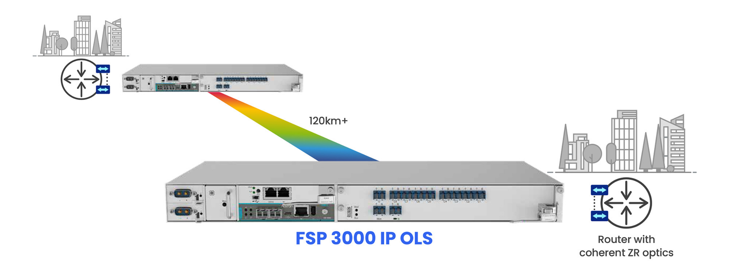
The second product is the FSP 3000 IP OLS, a compact open line system (OLS) designed for point-to-point links between sites 120km apart.
The OLS has been developed to simplify the setting up of dense wavelength division multiplexing (DWDM) optical links.
Enhancing broadband
Adtran has been developing a range of transceiver products to address specific requirements in the access-aggregation marketplace.
These include the MicroMux Edge Bidi, a QSFP+ pluggable module that supports 4×10 gigabit signals over 40km for mobile backhaul and enterprise wireless applications.
Adtran also offers the AccessWave25, a 25-gigabit tunable wavelength transceiver in an SFP28 form factor with a reach of 40km.
The pluggable module is used to link remote physical layer devices (RPDs) in cable operators’ networks. Cable operators are upgrading their infrastructure from 10 gigabits to 25 gigabits to support DOCSIS 4.0.
“You can argue if DOCSIS 4.0 is here or coming at the year-end,” says Saeid Aramideh, vice president of business development, optical engines business unit, at Adtran. “But there is no argument about the need for 25-gigabit uplinks for the cable MSO market.”
Now Adtran is announcing the AccessWave50, a 50-gigabit SFP56 optical module for fronthaul, part of the radio access network (RAN) and for other developments driving traffic such as smart homes, Internet of Things, and Smart Cities.
Aramideh refers to these applications as driving ‘enhanced’ broadband networks, requiring the upgrading of 25 gigabit links to 50- and even 100-gigabit ones.
Front-haul networks
For mobile, telco operators and RAN equipment makers are working with optical component makers to drive innovation in pluggables for emerging architectures such as enhanced 5G and 6G, says Aramideh.
In mobile networks, the front-haul network carries radio signals using the CPRI (common public radio interface) or enhanced CPRI protocols between the remote radio heads and the baseband units.
For 5G front-haul, the modules used are mainly at 10 gigabits-per-second (Gbps) with some 25-gigabit modules deployed. Adtran’s AccessWave50 addresses the next speed hike.
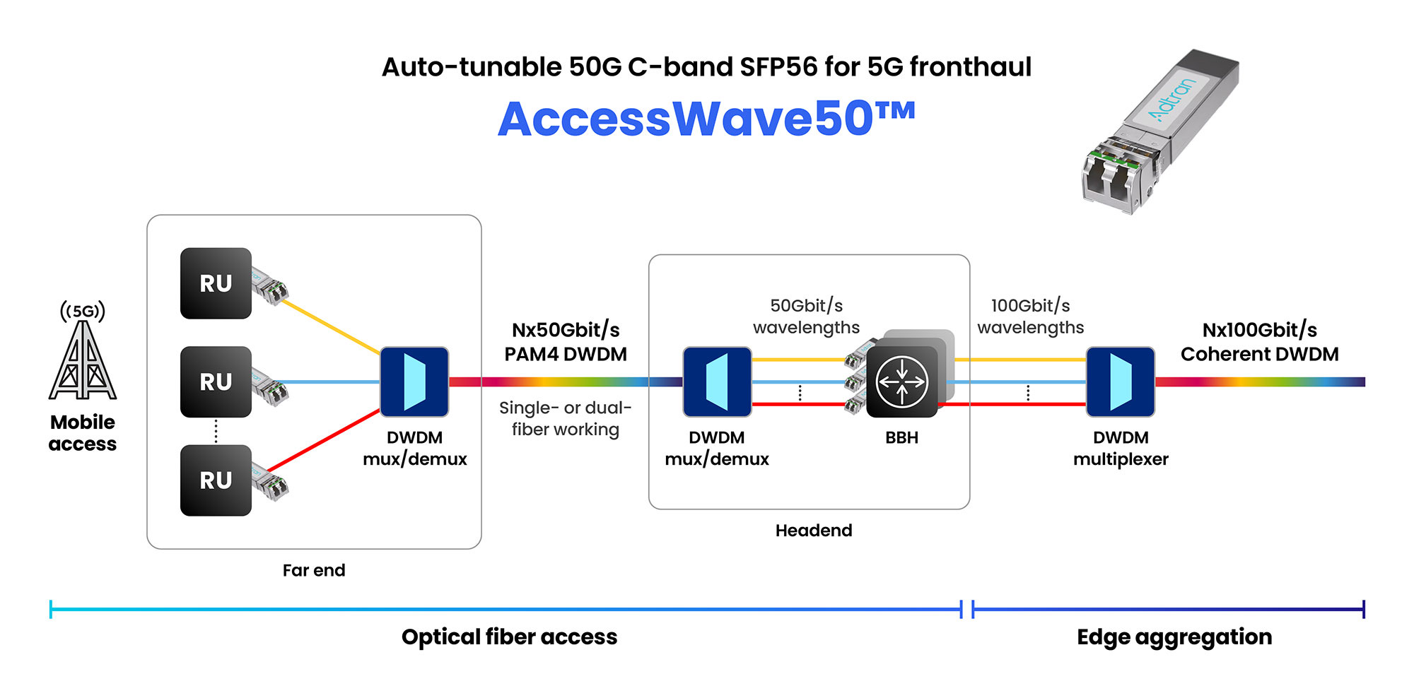
Adtran has designed the AccessWave50 using proprietary signal-shaping and distance optimisation techniques along with 4-level pulse amplitude modulation (PAM-4) to achieve the 50Gbps line rate.
“PAM-4 is proving itself to be a cost-performance-optimised technology and give you spectral efficiency as you go to higher data rates,” says Aramideh. “Of course, it’s not coherent optics, but you don’t need coherent for all applications.”
AccessWave50 uses a tunable laser and has a 15km, not 40km reach, but that is sufficient, says Aramideh, since front-haul networks are latency-constrained. The SFP56 module consumes 2.5W only.
Compact networking
Adtran has also unveiled its latest open line system (OLS) for C-band coherent transceivers.
The company has been providing bespoke OLS systems for hyperscalers. ADVA, the company Adtran acquired in 2022, provided Microsoft with the OLS that, working with the original ColorZ modules from Marvell, enabled 100 gigabit PAM-4 transmissions over 80km links.
Adtran also provides an OLS for data centre interconnects using 400ZR coherent modules for reaches of 120km.
The latest FSP 3000 IP OLS platform is a compact one-rack (1RU) high box that supports eight wavelengths over 120km.
The platform also includes an OTDR (optical time domain reflectometer) for fibre diagnostics.
The OLS can be used with 400-gigabit, 800-gigabit, and ultimately 1.6 terabit coherent pluggable modules once available.
The OLS is also designed for telecom metro interconnect networks. “Telcos, in response to AI, are also looking for OLS technology tailored to coherent transceivers,” says Stephan Rettenberger, senior vice president of marketing and corporate communications at Adtran.
A chief design challenge has been to fit the OLS into a 1 RU form factor, requiring integration and packaging work. The OLS has also been designed to be set up and operated straightforwardly.
The platform is scalable: two racks stacked double the wavelength counts to 16.
The FSP 3000 IP OLS product is already in the hands of one telco customer, says Rettenberger.

Broadcom’s silicon for the PCI Express 6.0 era
Broadcom has detailed its first silicon for the sixth generation of the PCI Express (PCIe 6.0) bus, developed with AI servers in mind.
The two types of PCIe 6.0 devices are a switch chip and a retimer.
Broadcom, working with Teledyne LeCroy, is also making available an interoperability development platform to aid engineers adopting the PCIe 6.0 standard as part of their systems.
Compute servers for AI are placing new demands on the PCIe bus. The standard no longer about connects CPUs to peripherals but also serving the communication needs of AI accelerator chips.
“AI servers have become a lot more complicated, and connectivity is now very important,” says Sreenivas Bagalkote, Broadcom’s product line manager for the data center solutions group.
Bagalkote describes Broadcom’s PCIe 6.0 switches as a ‘fabric’ rather than silicon to switch between PCIe lanes.
PCI Express
PCIe is an long-standing standard adopted widely, not only for computing and servers but across industries such as medical imaging, automotive, and storage.
The first three generations of PCIe evolved around the CPU. There followed a big wait for the PCIe 4.0, but since then, a new PCI generation has appeared every two years, each time doubling the data transfer rate.
Now, PCIe 6.0 silicon is coming to the market while work continues to progress on the latest PCIe 7.0, with the final draft ready for member review.
The PCIe standard supports various lane configurations from two to 32 lanes. For servers, 8-lane and 16-lane configurations are common.
“Of all the transitions in PCIe technology, generation 6.0 is the most important and most complicated,” says Bagalkote.
PCIe 6.0 introduces several new features. Like previous generations, it doubles the lane rate: PCIe 5.0 supports 32 giga-transfers a second (GT/s) while PCIe 6.0 supports 64GT/s.
The 64GT/s line rate requires the use of 4-level pulse amplitude modulation (PAM-4) for the first time; all previous PCIe generations use non-return-to-zero (NRZ) signalling.
Since PCIe must be backwards compatible, the PCIe 6.0 switch supports PAM-4 and NRZ signalling. More sophisticated circuitry is thus required at each end of the link as well as a forward error correction scheme, also a first for the PCIe 6.0 implementation.
Another new feature is flow control unit (FLIT) encoding, a network packet scheme designed to simplify data transfers.
PCIe 6.0 also adds integrity and data encryption (IDE) to secure the data on the PCIe links.
AI servers
A typical AI server includes CPUs, 8 or 16 interconnect GPUs (AI accelerators), network interface cards (NICs) to connect to GPUs making up the cluster, and to storage elements.
A typical server connectivity tray will likely have four switch chips, one for each pair of GPUs, says Bagalkote. Each GPU has a dedicated NIC, typically with a 400 gigabit per second (Gbps) interface. The PCIe switch chips also connect the CPUs and NVMe storage.
Broadcom’s existing generation PCIe 5.0 switch ICs have been used in over 400 AI server designs, estimated by the company at 80 to 90 per cent of all deployed AI servers.
Switch and retimer chips
PCIe 6.0’s doubling the lane data rate makes sending signals over 15-inch rack servers harder.
Broadcom says its switch chip uses serialiser-deserialiser (serdes) that outperform the PCIe specification by 4 decibels (dB). If an extra link distance is needed, Broadcom also offers its PCIe 6.0 retimer chips that also offer an extra 4dB.
Using Broadcom’s ICs at both ends results in a 40dB link budget, whereas the specification only calls for 32dB. “This [extra link budget] allows designers to either achieve a longer reach or use cheaper PCB materials,” says Bagalkote.
The PCIe switch chip also features added telemetry and diagnostic features. Given the cost of GPUs, such features help data centre operators identify and remedy issues they have, to avoid taking the server offline
“PCIe has become an important tool for diagnosing in real-time, remotely, and with less human intervention, all the issues that happen in AI servers,” says Bagalkote.
Early PCIe switches were used in a tree-like arrangement with one input – the root complex – connected via the switch to multiple end-points. Now, with AI servers, many devices connect to each other. Broadcom’s largest device – the PEX90144 – can switches between its 144 PCIe 6.0 lanes while supporting 2-, 4-, 8- or 16-lane-wide ports.
Broadcom also has announced other switch IC configurations with 104- and 88-lanes. These will be followed by 64 and 32 lane versions. All the switch chips are implemented using a 5nm CMOS process.
Broadcom is shipping “significant numbers” of samples of the chips to certain system developers.
PCIe versus proprietary interconnects
Nvidia and AMD that develop CPUs and AI accelerators have developed their own proprietary scale-up architectures. Nvidia has NVLink, while AMD has developed the Infinity Fabric interconnect technology.
Such proprietary interconnect schemes are used in preference to PCIe to connect GPUs, and CPUs and GPUs. However, the two vendors use PCIe in their systems to connect to storage, for example.
Broadcom says that for the market in general, open systems have a history of supplanting closed, proprietary systems. It points to the the success of its PCIe 4.0 and PCIe 5.0 switch chips and believes PCIe 6.0 will be no different.
Disaggregated system vendor developer, Drut Technologies, is now shipping a PCIe 5.0-based scalable AI cluster that can support different vendors’ AI accelerators. Its system uses Broadcom’s 144-lane PCIe 5.0 switch silicon for its interconnect fabric.
Drut is working on its next-generation PCIe 6.0-generation-based design.


OFC Rump Session: Reimagining global comms
Imagine a world plunged into digital silence. No texts, calls, emails, or internet.
At this year’s OFC conference in San Francisco, three teams of telecommunications experts will tackle a provocative thought experiment as part of the Rump Session: if Earth’s entire communication infrastructure vanished overnight, how would they rebuild it?
With a clean slate and ten years until implementation, the teams will outline what they consider is the ideal replacement global network.
The Rump Session’s audience will choose the best solution.
The scenario
OFC is asking the three teams of experts to imagine a world where global communication has been destroyed following an exceptional event.
Thankfully, only the network has been destroyed: manufacturing facilities, R&D sites, and communications expertise remain intact. So humanity has a chance to design a brand new network unencumbered by legacy equipment.
The ten-year implementation window is to allow emerging technologies to be considered as part of the new network build.
Considerations
Gazettabyte asked two telecom specialists outside the optical community how they would tackle the networking challenge.
If all the communications networks are down – fixed, mobile, satellite and broadcast – then it makes sense to get a simple universal comms system up and running as fast as possible, says William Webb, a consultant and author.
That would ensure there is enough communications to keep the population informed and allow those working on more complex systems to have communications while doing their design work.
For Dean Bubley, analyst and founder of Disruptive Analysis, the scenario triggers many questions.
Where will the demarcation point be between optical, wired and wireless networks?
“Is wireless just for the last kilometer or the last 10 meters of the access network?” says Bubley. “Or does wireless have a role for long-haul and transport as well, especially given the lower latency, and higher speed of light through air or a vacuum than through glass.”
Bubley wonders how to build in an expectation of continued innovation. Avoiding lock-in or static solutions is important: “Standards are fine, but there needs to be scope to try new things as well.”
Should Government oversee the restoration project or is the best approach to encourage competition and free market wherever possible? “Where does regulation fit and what does it focus on?” says Bubley.
Webb says the quickest way to get going is satellite coverage and portable antennas so people can use it when on the move even if it is nothing like as convenient as cellular.
The next stage would to launch High Altitude Platforms (HAPs) – tethered balloons and similar – to deliver cellular coverage relatively quickly.
A mix of tethered balloons near cities and high-altitude drones for other areas would deliver cellular comms within months, bringing cellular online at 4G-like capabilities.
“We can then work on a combined fixed-mobile solution. The ideal solution would have one fibre network delivering comms to homes, offices and cellular/Wi-Fi base stations, and one set of masts, ” says Webb.
Webb would forego network competition: it’s better to build a near-perfect network and then have a wholesale-retail split.
“Build from cities outwards, and stop building when the HAPs and satellite solution has the capacity to manage residual premises. Assume fibre to the edge of premises and Wi-Fi inside,” says Webb.
He would not rebuild cable networks or copper networks.
“But this sort of thing is best done by getting a group of us together and debating and discussing,” says Webb.
Just what the OFC Rump Session will do.
Origins
Antonio Tartaglia, one of this year’s Rump Session organisers, came up with the evening event’s theme.
“The Rump Session has always been my favourite OFC event. Joining the OFC Technical Program Committee, I was asked to contribute ideas,” says Tartaglia. “As a member of the public, I asked myself: ‘What is the Rump Session you’ve been dreaming of?’”
Tartaglia, system manager and expert in photonics technologies at Ericsson, is keen to learn what the teams of experts will come up with.
His educated guess is that optical technologies will take the lion’s share of the new network.
“It will also be hard to ignore low-earth orbit (LEO) satellite technology, that provides coverage where other technologies would not make economic sense,” says Tartaglia. Optical technologies will also play a big role here.
“But even in a brand-new world, I expect LEO satellites to complement, not replace terrestrial mobile networks as we know them,” says Tartaglia. “They are the result of decades of deep optimisation.”
“As scientists and engineers, we spend so much of our day-to-day work on improving the current state-of-the-art networks and taking that small next step forward in terms of technology, product or a solution,” says Dirk van den Borne, another of the Rump Session organisers.
He finds it intriguing to imagine how engineers would design the network if they could ignore existing installed equipment.
“This session will be thought-provoking and might spur great conversations at the conference and beyond,” says van den Borne, director of system engineering at Juniper Networks.
Rump Session details:
- When: April 1st Time:
- Evening time: 19:30 to 21:00
- Location: Rooms 203-204 (Level 2)
The Metaverse and the network
CTO interviews part 1: Stephen Alexander
“The inability to precisely predict how we’ll use it [the Metaverse], and how it will change our daily life, is not a flaw. Rather, it is a prerequisite for the Metaverse’s disruptive force.”
The Metaverse: And How it Will Revolutionize Everything by Matthew Ball, 2022.
CTO Interview
Stephen Alexander’s trusty 20-year-old dishwasher finally stopped working during the pandemic.
Unfortunately, getting spare parts shipped to the US was impossible, so Alexander, the CTO of Ciena (pictured), resorted to ‘how-to’ YouTube videos and got bits from eBay.
It highlighted the power of the online experience, something set to ramp significantly with the advent of the Metaverse.
The Metaverse refers to immersive virtual worlds where people will meet to socialise, learn, work and play.
During the pandemic, Ciena also experienced how the online experience can benefit work. The company used the network to guide remote data centre staff wearing virtual-reality headsets in operating its equipment.
Ciena also used high-resolution audio-visual equipment to continue development work during the pandemic. A solitary engineer in the lab would conduct measurements, sending the results to engineers working remotely.
“So we had started down this path where it [the Metaverse] is not just gaming but has got some interesting business applications,” says Alexander.
Metaverse survey
Ciena commissioned a recent survey on the Metaverse and its work uses. The systems vendor wanted to know how the customers of its customers view the emerging technology and how they would use it.
“What it [the Metaverse] represents for us is a use case,” says Alexander. “It’s an application space for this [networking] infrastructure we are all building.”
The study surveyed 15,000 people worldwide. Nearly all (96%) see the value of virtual meetings, while more than three-quarters (78%) say they would use more immersive experiences such as the Metaverse. However, two in five (38%) of the respondents said unreliable networking performance was a concern holding their organisations back.
Alexander, like many, spent his days in virtual meetings during the pandemic. In the mornings, he would talk to teams in Europe, in the middle of the day to the Americas, and in the evenings to the Asia Pacific. “It was a very efficient use of time,” he says.
But such tools are less effective for getting to know people. “You don’t have the ability to go to dinner, have coffee, go for a drink, that sort of thing,” he says.
Online meetings of up to 20 people are also limiting. Conversations are one-to-many unlike an in-person meeting where multiple parallel interactions occur.
“With a more immersive Metaverse environment where you have a virtual-reality capability, maybe we can start to do those things,” he says.
Alexander says that with the many areas of interactions, you can ask how many would be improved using augmented reality/ virtual reality.
Healthcare and education
Alexander experienced other benefits of online interactions, such as telemedicine, during the pandemic. But also some shortfalls. “What could have been done to improve the online education experience?” he says.
In a Metaverse-enabled world, education could enable high-school students to experience different types of work before deciding their career path. They could ‘join’ professionals – an airline pilot, a nurse, a doctor – to experience their working day.
“You plop on the headset, or you go into your ‘holodeck’ or advanced zoom environment and spend some hours or a day experiencing what that person’s life is like and what they do,” says Alexander. “That’s a huge educational potential enabled by this augmented reality/ virtual reality-enhanced world.”
Takeaways
One takeaway from Ciena’s commissioned survey is how widespread the acceptance of this future development is, says Alexander. There is also a broad interest in using the Metaverse for business applications.
The survey also highlighted some intriguing ideas.
Alexander says he looks forward to catching up with a former work colleague, but that this rarely happens due to their day-to-day commitments.
“You can imagine this world where his avatar and my avatar run into each other, and they talk about what’s going on in their lives and all the other things,” says Alexander. “And they come back, and we get a download from the evening.”
Network upshot
Alexander says that for some years, he has been saying that the network must get faster, the cloud has to get closer to the network edge, and infrastructure must get more intelligent.
These trends will benefit the Metaverse.
Latency is one crucial networking performance parameter.
Any end-device connected to the cloud has specific requirements regarding how it interacts and the latency it needs. For example, a latency of 100ms is ok when watching streaming video, but for gaming, that is too long; a headset requires a latency in the tens of milliseconds. Controlling an automated forklift truck is even more demanding. Here, tolerable latency is in single-digit milliseconds.
“That tells you, in some sense, where the edge of the cloud has to be,” says Alexander. “It just says that from the device to the cloud and back, it better be a certain physical distance as there is the speed of light issue.”
Network capacity also plays a role if the edge device generates enormous amounts of data – a petabyte, for example – and there is a timeliness to receiving an answer, even if it is a yes or no.
What network endpoints generate such massive amounts of data?
Alexander cites the example of synthesised designer drugs based on a person’s human genome. “If you have cancer, knowing that and getting the drug today, this week, this month is a whole lot different than getting it next year,” he says.
Other examples driving bandwidth he cites include military and agriculture (crops and livestock) applications.
“This is why this kind of a survey is so useful to us because we can go to our customers, whether they be cloud hyper-giants or to service providers and have a conversation about not what they are provisioning today, but what they’re going to provision in two to five years,” says Alexander.
This helps Ciena have better conversations with its customers about what they will need and should consider.
Planning
Staff at Ciena don’t yet have the word ‘Metaverse’ in their job titles.
Instead, staff are developing the next-generation WaveLogic coherent digital signal processor (DSP) family to drive the lowest cost-per-bit, highest capacity for fibre. Other Ciena employees are addressing network intelligence and automation; while others still are tackling routing, switching and the dynamic edge.
All applications require some flavour of these technologies, says Alexander.
The Metaverse is in its infancy in terms of use cases, with gaming being one prominant example.
“But you can imagine this can go for education, healthcare, and normal business interactions,” says Alexander. “It gets people’s juices flowing; look at the potential once we have high-capacity, low-latency connections to the cloud, and cloud is instantiated in enough local data centres that you can process things very quickly.”
Once that happens, people across industries will ask what they can do.
“That’s where you’re going to start to see the kind of the vectors of progress get established,” he says. “But common things that we see – capacity, connectivity, the ability to have a simpler, faster, more dynamic edge – those are key to enabling all this.”
Taking a unique angle to platform design

- A novel design based on a vertical line card shortens the trace length between an ASIC and pluggable modules.
- Reducing the trace length improves signal integrity while maintaining the merits of using pluggables.
- Using the vertical line card design will extend for at least two more generations the use of pluggables with Ethernet switches.
The travelling salesperson problem involves working out the shortest route on a round-trip to multiple cities. It’s a well-known complex optimisation problem.
Novel design that shortens the distance between an Ethernet switch chip and the front-panel optics
Systems engineers face their own complex optimisation problem just sending an electrical signal between two points, connecting an Ethernet switch chip to a pluggable optical module, for example.
Sending the high-speed signal over the link with sufficient fidelity for its recovery requires considerable electronic engineering design skills. And with each generation of electrical signalling, link distances are getting shorter.
In a paper presented at the recent ECOC show, held in Basel, consultant Chris Cole, working with Yamaichi Electronics, outlined a novel design that shortens the distance between an Ethernet switch chip and the front-panel optics.
The solution promises headroom for two more generations of high-speed pluggables. “It extends the pluggable paradigm very comfortably through the decade,” says Cole.
Since ECOC, there are plans to standardise the vertical line card technology in one or more multi-source agreements (MSAs), with multiple suppliers participating.
“This will include OSFP pluggable modules as well as QSFP and QSFP-DD modules,” says Cole.
Shortening links
Rather than the platform using stacked horizontal line cards as is common today, Cole and Yamaichi Electronics propose changing the cards’ orientation to the vertical plane.
Vertical line cards also enable the front-panel optical modules to be stacked on top of each other rather than side-by-side. As a result, the pluggables are closer to the switch ASIC; the furthest the high-speed electrical signalling must travel is three inches (7.6cm). The most distant span between the chip and the pluggable with current designs is typically nine inches (22.8cm).
“The reason nine inches is significant is that the loss is high as we reach 200 gigabits-per-second-per-lane and higher,” says Cole.
Current input-output proposals
The industry is pursuing several approaches to tackle such issues as the issues associated with high-speed electrical signalling and also input-output (I/O) bandwidth density.
One is to use twinaxial cabling instead of electrical traces on a printed circuit board (PCB). Such ‘Twinax’ cable has a lower loss, and its use avoids developing costly advanced-material PCBs.
Other approaches involve bringing the optics closer to the Ethernet switch chip, whether near-packaged optics or the optics and chip are co-packaged together. These approaches also promise higher bandwidth densities.
Cole’s talk focussed on a solution that continues using pluggable modules. Pluggable modules are a low-cost, mature technology that is easy to use and change.
However, besides the radio frequency (RF) challenges that arise from long electrical traces, the I/O density of pluggables is limited due to the size of the connector, while placing up to 36 pluggables on the 1 rack unit-high (1RU) front panel obstructs the airflow used for cooling.
Platform design
Ethernet switch chips double their capacity every two years. Their power consumption is also rising; Broadcom’s latest Tomahawk 5 consumes 500W.
The power supply a data centre can feed to each platform has an upper limit. It means fewer cards can be added to a platform if the power consumed per card continues to grow.
The average power dissipation per rack is 16kW, and the limit is around 32kW, says Cole. This refers to when air cooling is used, not liquid cooling.
He cites some examples.
A rack of Broadcom’s 12.8-terabit Tomahawk 3 switch chip – either with 32, 1RU or 16, 2RU cards with two chips per card – and associated pluggable optics consume over 30kW.
A 25.6-terabit Tomahawk 4-based chassis supports 16 line cards and consumes 28kW. However, using the recently announced Tomahawk 5, only eight cards can be supported, consuming 27KW.
“The takeaway is that rack densities are limited by power dissipation rather than the line card’s rack unit [measure],” says Cole.
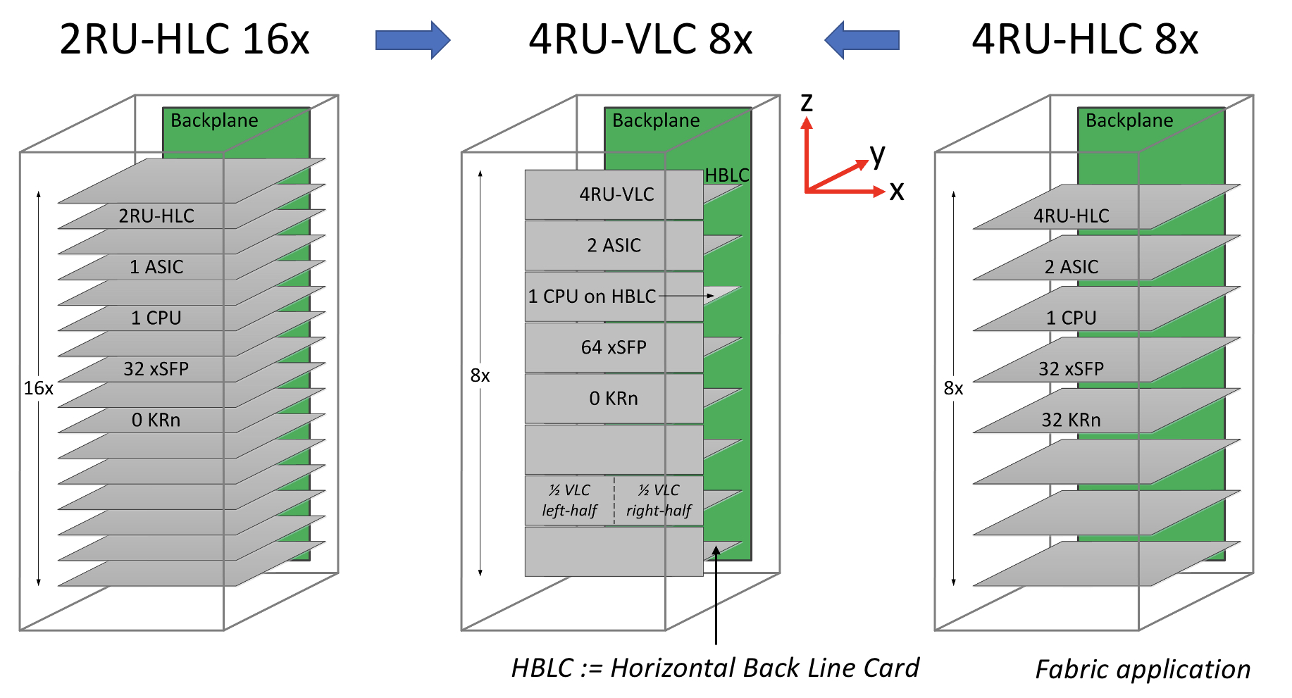
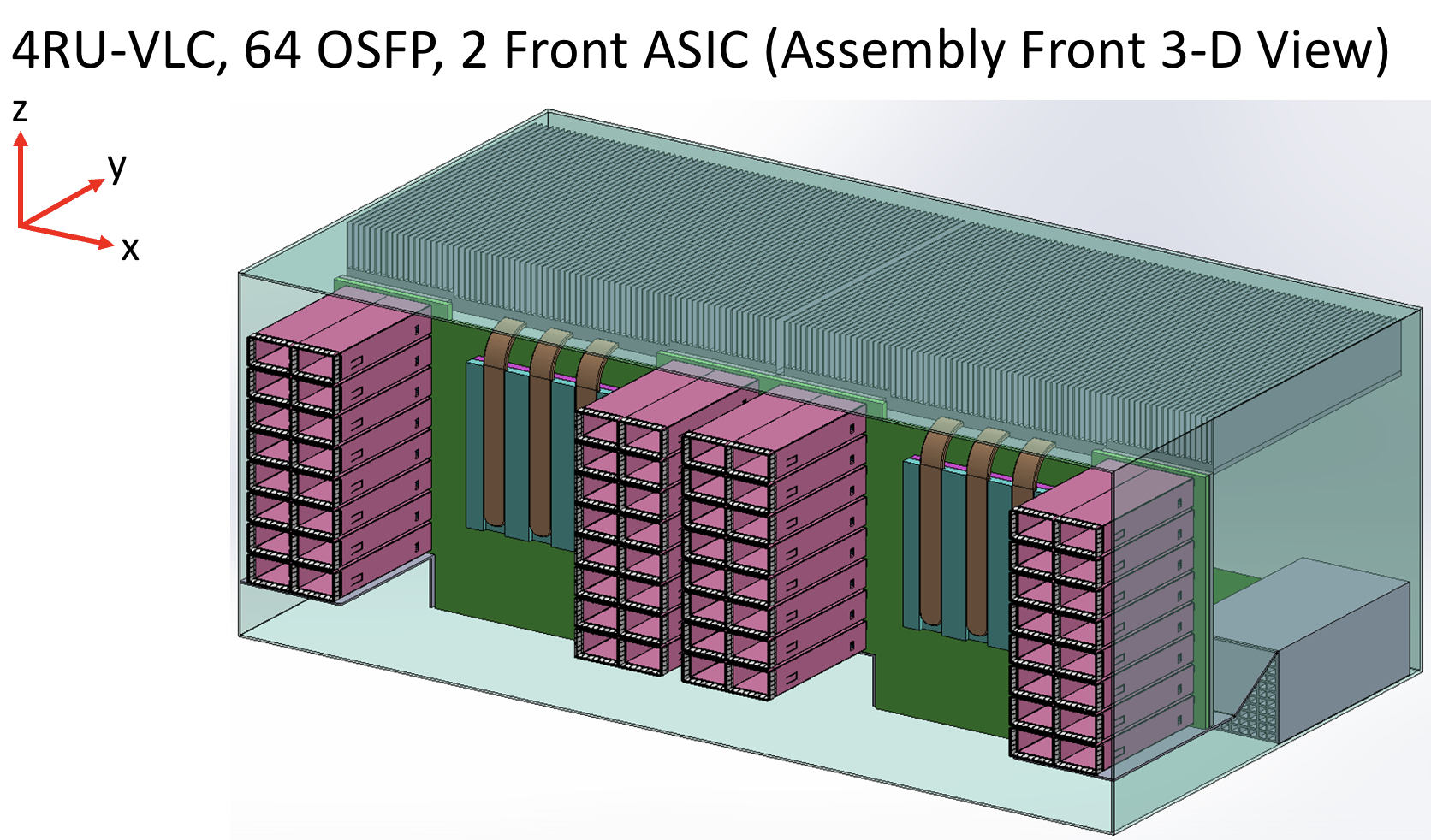
Vertical line card
The vertical line card design is 4RU high. Each card supports two ASICs on one side and 64 cages for the OSFP modules on the other.
A 32RU chassis can thus support eight vertical cards or 16 ASICs, equivalent to the chassis with 16 horizontal 2RU line cards.
The airflow for the ASICs is improved, enabling more moderate air fans to be used compared to 1RU or 2RU horizontal card chassis designs. There is also airflow across the modules.
“The key change in the architecture is the change from a horizontal card to a vertical card while maintaining the pluggable orientation,” says Cole.
As stated, the maximum distance between an ASIC and the pluggables is reduced to three inches, but Cole says the modules can be arranged around the ASIC to minimise the length to 2.5 inches.
Alternatively, if the height of the vertical card is an issue, a 3RU card can be used instead, which results in a maximum trace length of 3.5 inches. “[In this case], we don’t have dedicated air intakes for the CPU,” notes Cole.
Cole also mentioned the option of a 3RU vertical card that houses one ASIC and 64 OSFP modules. This would be suitable for the Tomahawk 5. However, here the maximum trace length is five inches.
Vertical connectors
Yamaichi Electronics has developed the vertical connectors needed to enable the design.
Cole points out that, unlike a horizontal connector, a vertical one uses equal-length contacts. This is not the case for a flat connector, resulting in performance degradation since a set of contacts has to turn and hence has a longer length.
Cole showed the simulated performance of an OSFP vertical connector with an insertion loss of over 70GHz.
“The loss up to 70GHz demonstrates the vertical connector advantage because it is low and flat for all the leads,” says Cole. “So this [design] is 200-gigabit ready.”
He also showed a vertical connector for the OSFP-XD with a similar insertion loss performance.
Also shown was a comparison with results published for Twinax cables. Cole says this indicates that the loss of a three-inch PCB trace is less than the loss of the cable.
“We’ve dramatically reduced the RF maximum length, so we had solved the RF roadblock problem, and we maintain the cost-benefit of horizontal line cards,” says Cole.
The I/O densities may be unchanged, but it preserves the mature technology’s benefits. “And then we get a dramatic improvement in cooling because there are no obstructions to airflow,” says Cole.
Vladimir Kozlov, CEO of the market research firm, LightCounting, wondered in a research note whether the vertical design is a distraction for the industry gearing up for co-packaged optics.
“Possibly, but all approaches for reducing power consumption on next-generation switches deserve to be tested now,” said Kozlov, adding that adopting co-packaged optics for Ethernet switches will take the rest of the decade.
“There is still time to look at the problem from all angles, literally,” said Kozlov

Lockheed Martin looks to pooling and optical I/O
Electronic systems must peer into ever-greater swathes of the electromagnetic spectrum to ensure a battlefield edge.
Michael HoffSuch electronic systems are used in ground, air, and sea vehicles and even in space.
The designs combine sensors and electronic circuitry for tasks such as radar, electronic warfare, communications and targeting.
Existing systems are custom designs undertaking particular tasks. The challenge facing military equipment makers is that enhancing such systems is becoming prohibitively expensive.
One proposed cost-saving approach is to develop generic radio frequency (RF) and sensor technology that can address multiple tasks.
“Now, each sensor will have to satisfy the requirements for all of the backend processing,” says Michael Hoff, senior research engineer at Lockheed Martin Advanced Technology Laboratories.
Such hardware will be more complex but upgrading systems will become simpler and cheaper. The generic sensors can also be assigned on-the-fly to tackle priority tasks as they arise.
“This is a foundational architectural shift that we see having relevance for many applications,” says Hoff.
Generic sensing
The proposed shift in architectural design was discussed in a paper presented at the IEEE International Symposium on Phased Array Systems and Technology event held in October.
Co-authored by Lockheed Martin and Ayar Labs, the paper focuses on generic sensing and the vast amount of data it generates.
Indeed, the data rates are such that optical interconnect is needed. This is where Ayar Labs comes in with its single-die electro-optical I/O chiplet.
Lockheed Martin splits sensing into two categories: RF sensing and electro-optic/ infrared (or EO/IR). Electro-optic sensors are used for such applications as high-definition imaging.
“When we talk about platform concepts, we typically lump EO/IR into one category,” says Hoff. The EO/IR could be implemented using one broadband sensor or with several sensors, each covering specific wavelengths.
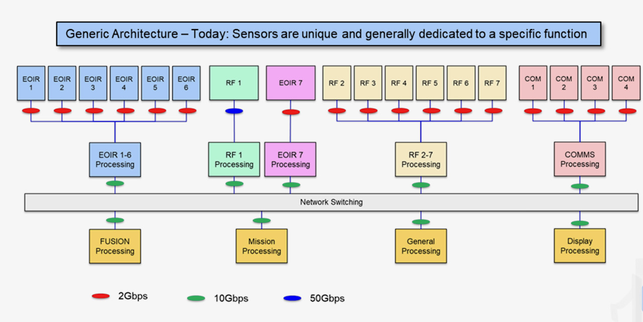
A representation of current systems is shown above. Here, custom designs comprising sensors, analogue circuitry, and processing pass data to mission-processing units. The mission equipment includes data fusion systems and displays.
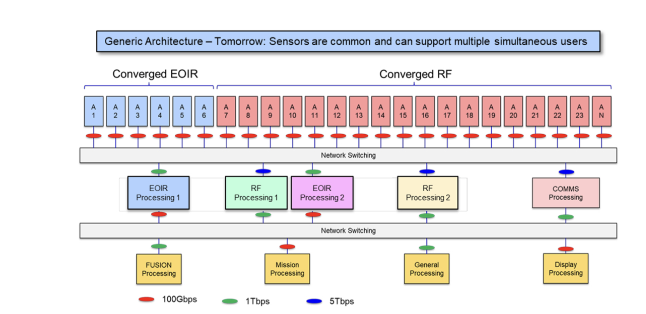
Lockheed Martin proposed architecture uses two generic sensor types – RF and EO/IR – which can be pooled as required (see diagram below).
For example, greater resources may need to be diverted urgently to the radar processing at the expense of communications that can be delayed.
“It’s a more costly individual development, but because it can be shared across different applications and in different teams, cost savings come out ahead,” says Hoff.
An extra networking layer is added to enable the reconfigurability between the sensors and the mission functions and processing systems that use, process, and digest the dat
Optical interconnect
Data traffic generated by modern military platforms continues to rise. One reason is that the frequencies sensed are approaching millimetre-wave. Another is that phased-array systems are using more elements so that more data streams must be be digitised and assessed.
Lockheed Martin cites as an example a military platform comprising 16 phased-array antennas, each with 64 elements.
Each element is sampled with a 14-bit, 100 gigasample-per-second analogue-to-digital converter. The data rate is further doubled since in-phase and quadrature channels are sampled. Each phased array thus generates 179.2 terabits-per-second (Tbps) while the total system data is 2.87 petabits-per-second.
Algorithms at the sensor source can trim the raw data by up to 256x, reducing each antenna’s data stream to 700Gbps, or 11.2Tbps overall.
Optical communications is the only way to transport such vast data flows to the mission processors, says Lockheed Martin.
Multi-chip modules
Any interconnect scheme must not only transfer terabits of data but also be low power and compact.
“The size, weight and power constraints, whether an optical transceiver or processing hardware, get more constrained as you move towards the sensor location,” says Hoff.
The likelihood is that integrated photonics is going to be required as bandwidth demand increases and as the interconnect gets closer to the sensor, he says.
Lockheed Martin proposes using a multi-chip module design that includes the optics, in this case, Ayar Labs’s TeraPhy chiplet.
The TeraPhy combines electrical and silicon photonics circuitry on a single die. Overall, the die has eight transceiver circuits, each supporting eight wavelengths. In turn, each wavelength carries 32 gigabit-per-second (Gbps) of data such that the 54mm2 die transmits 2Tbps in total.
Lockheed Martin has compared its proposed multi-chip module design that includes integrated optics with a discrete solution based on mid-board optics.
The company says integrated optics reduced the power consumed by 5x, from 224W to 45W, while the overall area is reduced a dozen fold, from 3,527 mm2 to 295mm2.
“You’re going to need optical interconnects at many different points,” says Hoff; the exact locations of these multi-chip modules being design-dependent.
Charles Wuischpard, CEO of Ayar Labs, points out that the TeraPhy is built using macro blocks to deliver 2Tbps.
“There are customer opportunities that require far less bandwidth, but what they want is a very tiny chip with very low energy consumption on the input-output [I/O] transport,” says Wuischpard. “There are different areas where the size, weight and power benefits come into play, and it may not all be with our single chiplet solution that we offer.”
Investor
Lockheed Martin became a strategic investor in Ayar Labs in 2019.
“We see this [Ayar Labs’ optical I/O technology] as a foundational technology that we want to be out in front of and want to be first adopters of,” says Hoff.

BT's IP-over-DWDM move
- BT will roll out next year IP-over-DWDM using pluggable coherent optics in its network
- At ECOC 2022, BT detailed network trials that involved the use of ZR+ and XR optics coherent pluggable modules
Telecom operators have been reassessing IP-over-DWDM with the advent of 400-gigabit coherent optics that plug directly into IP routers.
According to BT, using pluggables for IP-over-DWDM means a separate transponder box and associated ‘grey’ (short-reach) optics are no longer needed.
Until now, the transponder has linked the IP router to the dense wavelength-division multiplexing (DWDM) optical line system.
“Here is an opportunity to eliminate unnecessary equipment by putting coloured optics straight onto the router,” says Professor Andrew Lord, BT’s head of optical networking.
Removing equipment saves power and floor space too.
DWDM trends
Operators need to reduce the cost of sending traffic, the cost-per-bit, given the continual growth of IP traffic in their networks.
BT says its network traffic is growing at 30 per cent a year. As a result, the operator is starting to see the limits of its 100-gigabit deployments and says 400-gigabit wavelengths will be the next capacity hike.
Spectral efficiency is another DWDM issue. In the last 20 years, BT has increased capacity by lighting a new fibre pair using upgraded optical transport equipment.
Wavelength speeds have gone from 2.5 to 10, then to 40, 100, and soon 400 gigabits, each time increasing the total traffic sent over a fibre pair. But that is coming to an end, says BT.
“If you go to 1.2 terabits, it won’t go as far, so something has to give,” says Lord. ”So that is a new question we haven’t had to answer before, and we are looking into it.”
Fibre capacity is no longer increasing because coherent optical systems are already approaching the Shannon limit; send more data on a wavelength and it occupies a wider channel bandwidth.
Optical engineers have improved transmission speeds by using higher symbol rates. Effectively, this enables more data to be sent using the same modulation scheme. And keeping the same modulation scheme means existing reaches can still be met. However, upping the symbol rate is increasingly challenging.
Other ways of boosting capacity include making use of more spectral bands of a fibre: the C-band and the L-band, for example. BT is also researching spatial division multiplexing (SDM) schemes.
IP-over-DWDM
IP-over-DWDM is not a new topic, says BT. To date, IP-over-DWDM has required bespoke router coherent cards that take an entire chassis slot, or the use of coherent pluggable modules that are larger than standard QSFP-DD client-side optics ports.
“That would affect the port density of the router to the point where it’s not making the best use of your router chassis,“ says Paul Wright, optical research manager at BT Labs.
The advent of OIF-defined 400ZR optics has catalysed operators to reassess IP-over-DWDM.
The 400ZR standard was developed to link equipment housed in separate data centres up to 120km apart. The 120km reach is limiting for operators but BT’s interest in ZR optics stems from the promise of low-cost, high-volume 400-gigabit coherent optics.
“It [400ZR optics] doesn’t go very far, so it completely changes our architecture,” says Lord. “But then there’s a balance between the numbers of [router] hops and the cost reduction of these components.”
BT modelled different network architectures to understand the cost savings using coherent ZR and ZR+ optics; ZR+ pluggables have superior optical performance compared to 400ZR.
The networks modelled included IP routers in a hop-by-hop architecture where the optical layer is used for point-to-point links between the routers.
This worked well for traffic coming into a hub site but wasn’t effective when traffic growth occurred across the network, says Wright, since traffic cascaded through every hop.
BT also modelled ZR+ optics in a reconfigurable optical add-drop multiplexer (ROADM) network architecture, as well as a hybrid arrangement using both ZR+ and traditional coherent optics. Traditional coherent optics, with its superior optical performance, can pass through a string of ROADM stages where ZR+ optics falls short.
BT compared the cost of the architectures assuming certain reaches for the various coherent optics and published the results in a paper presented at ECOC 2020. The study concluded that ZR and ZR+ optics offer significant cost savings compared to coherent transponders.
ZR+ pluggables have since improved, using higher output powers to better traverse a network’s ROADM stages. “The [latest] ZR+ optics should be able to go further than we predicted,” says Wright.
It means BT is now bought into IP-over-DWDM using pluggable optics.
BT is doing integration tests and plans to roll out the technology sometime next year, says Lord.
XR optics
BT is a member of the Open XR Forum, promoting coherent optics technology that uses optical sub-carriers.
Dubbed XR optics, if all the subs-carriers originate at the same point and are sent to a common destination, the technology implements a point-to-point communication scheme.
Sub-carrier technology also enables traffic aggregation. Each sub-carrier, or a group of sub-carriers, can be sent from separate edge-network locations to a hub where they are aggregated. For example, 16 endpoints, each using a 25-gigabit sub-carrier, can be aggregated at a hub using a 400-gigabit XR optics pluggable module. Here, XR optics is implementing point-to-multipoint communication.
Lord views XR optics as innovative. “If only we could find a way to use it, it could be very powerful,” he says. “But that is not a given; for some applications, XR optics might be too big and for others it may be slightly too small.”
ECOC 2022
BT’s Wright shared the results of recent trial work using ZR+ and XR optics at the recent ECOC 2022 conference, held in Basel in September.
The 400ZR+ were plugged into Nokia 7750 SR-s routers for an IP-over-DWDM trial that included the traffic being carried over a third-party ROADM system in BT’s network. BT showed the -10dBm launch-power ZR+ optics working over the ROADM link.
For Wright, the work confirms that 0dBm launch-power ZR+ optics will be important for network operators when used with ROADM infrastructures.
BT also trialled XR optics where traffic flows were aggregated.
“These emerging technologies [ZR+ and XR optics] open up for the first time the ability to deploy a full IP-over-DWDM solution,” concluded Wright.
ECOC '22 Reflections - Final Part
Gazettabyte has been asking industry and academic figures for their thoughts after attending ECOC 2022, held last month in Basel, Switzerland. In particular, what developments and trends they noted, what they learned, and what, if anything, surprised them.
In the final part, Dr. Sanjai Parthasarathi of Coherent, Acacia’s Tom Williams, ADVA’s Jörg-Peter Elbers and Fabio Pittalà of Keysight Technologies share their thoughts.
Dr. Sanjai Parthasarathi, Chief Marketing Officer, Coherent
The ECOC event represents an excellent opportunity for us – a vertically-integrated manufacturer selling at all levels of the value chain – to meet with customers, end-customers and partners/ suppliers.
There was a refreshing sense of optimism and excitement for optical communications, driven by relentless bandwidth growth, despite the macroeconomic backdrop.
The roadmap for optical transceivers is dictated by the electrical interface used for Ethernet switch chips. We have seen that play out yet again for 100-gigabit electrical lanes used for 25-terabit and 50-terabit Ethernet switches.
Several transceiver suppliers demonstrated products with 100 gigabit-per-lane electrical interfaces in quad and octal form factors. The optical lane of a transceiver typically begins at the same speed as the electrical lane and then progresses to a faster rate. This transition should be expected for 800-gigabit transceivers as well.
While 100 gigabit-per-lane transceivers, such as the 800G-DR8 and the 2x400G-FR4 devices, there were devices demonstrated that enable the transition to optical 200-gigabit lanes. It was satisfying to see a warm response for the demonstration of Coherent’s 200-gigabit electro-absorption modulated laser (EML) and Semtech’s 200-gigabit EML driver. I am confident that direct detection will play a predominant role in 800-gigabit and 1.6-terabit data centre links.
Despite the great interest in co-packaged optics, nearly all the working demonstrations at the show used pluggable transceiver modules. Industry colleagues are preparing for pluggable transceiver modules using the next 200-gigabit electrical interface. Indeed, at ECOC, there was an OIF-CEI 224G demo by Keysight and Synopsys.
One key topic at the show concerned whether ‘coherent lite’ or direct detect is the preferred solution for data centres and edge aggregation. The debate remains open and no one solution fits all. It will depend on the specific application and architecture. A broad portfolio supported by different technology platforms frees you to select the best approach to serve the customer’s needs.
I saw the industry responding to the need for disaggregation and innovative solutions for access and telecom. Coherent’s 100G ZR announcement is one such example, as well as the extra performance of high-power 400ZR+ coherent transceivers.
We started this trend and we now see others announcing similar solutions.
Arista’s demo, which featured 400ZR connections over a 120km data centre interconnect (DCI) link, enabled by our pluggable optical line system in a QSFP form factor, received much attention and interest.
Tom Williams, Senior Director of Marketing for Acacia, now part of Cisco.
Many of us are still of a mindset where any opportunity to get together and see industry friends and colleagues is a great show.
My focus is very much on the success of 400-gigabit pluggable coherent solutions.
We’ve been talking about these products for a long time, back to the initial OIF 400ZR project starting in late 2016. Since then, 400ZR/ZR+ has been a hot topic at every conference.
The commercial success of these solutions, and the impact that they’re having on network architectures, has been gratifying. These products have ramped in volumes not seen by any previous coherent technology.
The industry has done a great job at 400 gigabits, striking the right balance of power and performance. Now, we’re looking at 800 gigabits and working through some of the same questions. Discussions around 1.6 terabits have even started.
Much work is still required but what we heard from customers at ECOC is that the trend toward pluggable coherent will likely continue.
Jörg-Peter Elbers, Senior Vice President, Advanced Technology, Standards and IPR at ADVA
‘Never say never’ captures well ECOC’s content. There was no one groundbreaking idea but topics discussed in the past are back on the agenda, either because of a need or the technology has progressed.
Here are several of my ECOC takeaways:
- The 130 gigabaud (GBd) class of coherent optics is coming, and the generation after that – 240GBd – is on the horizon.
- Coherent optics continue to push towards the edge. Will there be a Very-High Speed Coherent PON after 50G High-Speed PON?
- Whether co-packaged optics or front-pluggable modules, electro-photonic integration is rapidly advancing with some interesting industry insights shared at the conference.
- Quantum-safe communication is becoming part of the regular conference program.
- Optical Satcom is gaining traction. Optical ground-to-space links are promising yet challenging.
Fabio Pittalà, Product Planner, Broadband and Photonics – Center of Excellence, Keysight Technologies
This was my first ECOC as an employee of Keysight. I spent most of my time at the exhibition introducing the new high-speed Keysight M8199B Arbitrary Waveform Generator.
There were a lot of discussions focusing on technologies enabling the next Ethernet rates. There is a debate about intensity-modulation direct detection (IMDD) versus coherent but also what modulation format, symbol rate or degree of parallelisation.
While the industry is figuring out the best solution, researchers achieved important milestones by transmitting the highest symbol rate and the highest net bitrate.
Nokia Bell-Labs demonstrated record-breaking transmission of 260-gigabaud dual-polarisation quadrature phase-shift keying (DP-QPSK) over 100km single-mode fibre.
Meanwhile, NTT broke the net bitrate record by transmitting more than 2 terabit-per-second using a probabilistic-constellation-shaped dual-polarisation quadrature amplitude modulation (DP-QAM) over different data centre links.