
Data centre photonics - an ECOC report

- ECOC 2022 included talks on optical switching and co-packaged optics.
- Speakers discussed optical switching trends and Google’s revelation that it has been using optical circuit switching in its data centres.
- Nvidia discussed its latest chips, how they are used to build high-performance computing systems, and why optical input-output will play a critical role.
Co-packaged optics and optical switching within the data centre were prominent topics at the recent ECOC 2022 conference and exhibition in Basel, Switzerland.
There were also two notable data centre announcements before ECOC.
Tencent announced it would adopt Broadcom’s Humboldt design, a hybrid co-packaged optics version of the Tomahawk 4 switch chip, in its data centres. Tencent is the first hyperscaler to announce it is adopting co-packaged optics.
Google also revealed its adoption of optical circuit switching in its data centres. Google made the revelation in a paper presented at the Sigcomm 2022 conference held in Amsterdam in August.
Optical circuit switching
Google rarely details its data centre architecture, but when it does, it is usually at Sigcomm.
Google first discussed a decade of evolution of its ‘Jupiter’ data centre architecture in a paper at Sigcomm in 2015.
This year, Google gave an update revealing that it has been using optical circuit switching in its data centres for the past five years. As a result, Google can scale its data centre more efficiently using a reconfigurable optical layer.
Upgrading a data centre’s network is much more complex than upgrading servers and storage. Moreover, a data centre is operational far longer than each generation of equipment. It is thus hard for a data centre operator to foresee how equipment and workloads will evolve over the data centre’s lifetime, says Google.
Google would pre-deploy the spine layer when it started operating a data centre. For Google’s Jupiter architecture, 64 spine blocks, each using 40 gigabit-per-second (Gbps) links, would be deployed. Then, Google added newer aggregation blocks with 100Gbps links. But the hyperscaler could not fully benefit due to the pre-existing 40Gbps spine links.
Google wanted to avoid touching the spine switches. A partial upgrade would have limited benefits, while fully upgrading the spine would take months and be hugely disruptive and costly.
Google’s first solution introduced a MEMS-based optical circuit switching layer between the aggregation and spine blocks.
The MEMS-based switch is data rate agnostic and can support multiple generations of optical modules. The switch’s introduction also allowed Google to add new spine blocks alongside new aggregation blocks; the hyperscaler no longer had to pre-deploy the spine.
At some point, Google decided that for new data centre builds, it would use optical circuit switching only and remove the spine layer of electrical switches.
Adopting optical circuit switch-based interconnect changes Google’s data centres from a clos to a direct-connect architecture. However, not all paths are direct; some take two hops to link aggregation blocks.
Google has developed sophisticated control software to best exploit the direct connectivity for traffic flows.
The software also adapts the network topology – the optical links between the aggregation blocks and their capacities. Such topology changes occur every few weeks, with the system first learning the nature of the traffic and workloads.
Removing the spine layer and replacing it with optical circuit switches has reduced Google’s data centre networking costs by 30 per cent and power consumption by 41 per cent.
ECOC reflections about Google’s optical switch adoption
There was much discussion at ECOC of Google’s use of optical circuit switching in its data centres.
S.J. Ben Yoo, a distinguished professor at the University of California, Davis, gave an ECOC talk about new trends in optical switching. “These are expected future trends,” he said. “I don’t have a crystal ball.”
Prof. Ben Yoo stressed the difficulty of scaling up and scaling out data centre networking architectures in the era of artificial intelligence workloads.
He described co-packaged optics as ‘Trend 0’ because it only delivers bandwidth (input-output capacity).
In contrast, introducing a reconfigurable optical switching layer on top of electrical aggregation switches is the first trend in optical switching. This is what Google has done with its optical circuit switch.
The next development in the data centre, says Ben Yoo, will be the introduction of photonic integrated circuit-based optical switching.
Huawei’s Maxim Kuschnerov, in his ECOC talk, said optical switching in the data centre would only grow in importance.
“Are there use cases where we can use optical switching and what are they?” he said. “I like to take a use-case perspective and find a technology that fulfils that use case.”
His view is that with the classical clos architecture, you can’t just rip out a single layer of electrical switches and replace it with optical ones. “There is a reason why you need all these switches and aggregation functionality,” says Kuschnerov.
Kuschnerov views Google’s optical circuit switching as nothing more than an automated patch panel.
“This is not the optical switch which is the saviour of future data centres,” he says.
Mark Filer, optical network architect, systems and services infrastructure at Google, in an ECOC tutorial detailing how Google uses and benefits from standards, multi-source agreements and open-source developments, was asked about Google’s custom optical switch.

How could Google explain such a custom design if the hyperscaler is such a proponent of open standards? And would Google consider contributing its optical circuit switch and software design to an open community framework?
“My guess is over time, we may see that it finds its way into some kind of open framework,” said Filer, adding that right now, Google sees its optical circuit switch as delivering a competitive advantage.
Co-packaged optics
Benjamin Lee, a senior research scientist at Nvidia, in his ECOC address, discussed the high-performance computing market and the role graphics processing units (GPUs) play in accelerating artificial intelligence and machine learning tasks.
Nvidia not only develops processors, GPUs and data processing unit ICs but also networking silicon and systems that the company uses to make high-performance computing systems.
Lee’s talk addressed the role optical interconnect will play in ensuring continuing scaling of high-performance GPU-based computing systems.
Scaled systems
Nvidia’s latest GPU, announced earlier this year, is the 80-billion-transistor Hopper H100. The H100 deliver a six-fold improvement in throughput compared to Nvidia’s existing A100 GPU announced in 2020.
The Hopper is Nvidia’s first GPU that uses the latest generation of stacked DRAM memory, known as high bandwidth memory 3 (HBM3). In addition, Hopper also uses Nvidia’s fourth-generation NVlink interface.
Eight H100 GPUs fit within Nvidia’s DGX box, as do four Nvidia NVSwitches used to interconnect the GPUs. In addition, an Nvidia Superpod connects 32 DGX nodes – 256 GPUs – using an external tier of NVSwitches.
“A paradigm shift we’re seeing is that switched interconnect is becoming important for scale-up,” said Lee. “So when we want to make the node more computationally powerful, those switches are being put inside the box to connect the GPUs.”
Switch ASIC bandwidths are consistently improving, with 51.2-terabit switch silicon being state-of-the-art. But despite such progress, the scaling is insufficient to keep up with bandwidth requirements, said Lee.
Switch ASIC power consumption is also rising, with advanced CMOS scaling having less impact on designs. Lee foresees switch ASICs consuming 2kW if current trends continue.
In turn, ASIC input-output (I/O) accounts for an increasing portion of the chip’s overall power consumption.
This is true for Nvidia’s GPUs and switch chips, so any I/O technology developed for switching will also benefit its GPUs.
Thus, Nvidia sees optical I/O as the key to scaling the processing performance of its ASICs and computing systems.
I/O metrics
Lee outlined various metrics when discussing optical I/O:
- the electrical interfaces used between the ASIC and optics, and their reach
- the power consumption of the module (the chip, and the chip and optics)
- the system power (of the line card or platform)
- interface density: the capacity exiting a millimetre of surface in terabits-per-second-per-mm (Tbps/mm)
For a system using a 102.4-terabit switch IC, half the power is consumed by the ASIC and half by the edge-board pluggable optics. Here the OIF’s long reach (LR) interface links the two.
The chip’s electrical interfaces consume 4.5 to 6.5 picojoule-per-bit (pJ/b) such that the total switch IC I/O power consumed is 450W.
The next step is co-packaged optics. Here, optical chiplets are placed closer to the ASIC (100mm away) such that the OIF’s lower power XSR (extra short reach) interface can be used that consumes 1.24-1.7pJ/s, says Lee.
Again taking a module view, Nvidia views the co-packaged design as comprising two electrical interfaces (the XSR interface between the chip and optical chiplets either side) and one optical interface.
This equates to 250W per chip module, a modest power saving at the chip module level but a significant power saving at the system level, given the optics is now part of the module.
However, bandwidth density is 475-870Gbps/mm, and for beyond 100-terabit switches, a further fourfold improvement is needed: 2Tbps/mm and, ultimately, 10Tbps/mm.
Just achieving a 2Tb/s/mm interface density will be challenging, says Lee.
For that, 2.5D co-packaged optics will be needed with the ASIC and chiplets sharing a silicon interposer that enables higher wire densities.
2.5D integration is already an established technology in the semiconductor industry; Nvidia has been using the technology for its GPUs since 2016.
The technology enables much closer coupling between the ASIC and optics (some 1mm), resulting in sub 1pJ/bit. Nvidia cites research showing a 0.3pJ/b has already been achieved.
Scaling I/O
Lee outlined all the ways I/O can be scaled.
Baud rate is one approach, but the energy efficiency diminishes as the symbol rate increases, from 50 to 100 to 200 gigabaud.
Modulation is another approach, moving from non-return-to-zero to 4-level pulse amplitude modulation (PAM-4) and even higher PAM schemes. The challenge is that the signal-to-noise ratio diminishes the higher the PAM scheme, requiring additional digital signal processing which, in turn, consumes more power.
Another technique, polarization, can be used to double the data rate. Then there is the spatial domain. Here, tighter pitches can be used, says Lee, moving from 250, 127 and even 80 microns before other approaches are needed. These include multi-core fibre, waveguide fan-outs and even bidirectional optics (what Google uses for its optical circuit switch ports, to save on fibre and port count).
All these spatial approaches require considerable development and operational costs, says Lee.
The most promising way to boost throughput and increase interface density is using wavelength division multiplexing (WDM).
Nvidia has produced several generations of test chips that use wavelength parallelism in the O-band based on micro-ring resonators.
Nvidia’s steer
Micro-ring resonator technology already supports 100Gbps modulation rates. The optical circuit is also compact, energy-efficient and supports wavelength scaling.
Lee also outlined other key technologies that will be needed, each bringing their own challenges. One is the external laser source, another is advanced packaging.
Nvidia believes that for future generations of ASICs, dense WDM mirror-ring modulated links offer the most promising approach to meeting both low power and the massive interface density improvements that will be needed.
This will require low-cost lasers while packaging remains a severe challenge.
2.5D integration is going to be an important step in the evolution of switch interconnect, concluded Lee.

ECOC '22 Reflections - Part 3

Gazettabyte is asking industry and academic figures for their thoughts after attending ECOC 2022, held in Basel, Switzerland. In particular, what developments and trends they noted, what they learned, and what, if anything, surprised them.
In Part 3, BT’s Professor Andrew Lord, Scintil Photonics’ Sylvie Menezo, Intel’s Scott Schube, and Quintessent’s Alan Liu share their thoughts.
Professor Andrew Lord, Senior Manager of Optical Networks Research, BT
There was strong attendance and a real buzz about this year’s show. It was great to meet face-to-face with fellow researchers and learn about the exciting innovations across the optical communications industry.
The clear standouts of the conference were photonic integrated circuits (PICs) and ZR+ optics.
PICs are an exciting piece of technology; they need a killer use case. There was a lot of progress and discussion on the topic, including an energetic Rump session hosted by Jose Pozo, CTO at Optica.
However, there is still an open question about what use cases will command volumes approaching 100,000 units, a critical milestone for mass adoption. PICs will be a key area to watch for me.
We’re also getting more clarity on the benefits of ZR+ for carriers, with transport through existing reconfigurable optical add-drop multiplexer (ROADM) infrastructures. Well done to the industry for getting to this point.
All in all, ECOC 2022 was a great success. As one of the Technical Programme Committee (TPC) Chairs for ECOC 2023 in Glasgow, we are already building on the great show in Basel. I look forward to seeing everyone again in Glasgow next year.
Sylvie Menezo, CEO of Scintil Photonics
What developments and trends did I note at ECOC? There is a lot of development work on emergent hybrid modulators.
Scott Schube, Senior Director of Strategic Marketing and Business Development, Silicon Photonics Products Division at Intel.
There were not a huge amount of disruptive announcements at the show. I expect the OFC 2023 event will have more, particularly around 200 gigabit-per-lane direct-detect optics.
Several optics vendors showed progress on 800 gigabit/ 2×400 gigabit optical transceiver development. There are now more vendors, more flavours and more components.
Generalising a bit, 800 gigabit seems to be one case where the optics are ready ahead of time, certainly ahead of the market volume ramp.
There may be common-sense lessons from this, such as the benefits of technology reuse, that the industry can take into discussions about the next generation of optics.
Alan Liu, CEO of Quintessent
Several talks focused on the need for high wavelength count dense wavelength division multiplexing (DWDM) optics in emerging use cases such as artificial intelligence/ machine learning interconnects.
Intel and Nvidia shared their vision for DWDM silicon photonics-based optical I/O. Chris Cole discussed the CW-WDM MSA on the show floor, looking past the current Ethernet roadmap at finer DWDM wavelength grids for such applications. Ayar Labs/Sivers had a DFB array DWDM light source demo, and we saw impressive research from Professor Keren Bergman’s group.
An ecosystem is coalescing around this area, with a healthy portfolio and pipeline of solutions being innovated on by multiple parties, including Quintessent.
The heterogeneous integration workshop was standing room only despite being the first session on a Sunday morning.
In particular, heterogeneously integrated silicon photonics at the foundry level was an emergent theme as we heard updates from Tower, Intel, imec, and X-Celeprint, among other great talks. DARPA has played – and plays – a key role in seeding the technology development and was also present to review such efforts.
Fibre-attach solutions are an area to watch, in particular for dense applications requiring a high number of fibres per chip. There is some interesting innovation in this area, such as from Teramount and Suss Micro-Optics among others.
Shortly after ECOC, Intel also showcased a pluggable fibre attach solution for co-packaged optics.
Reducing the fibre packaging challenge is another reason to employ higher wavelength count architectures and DWDM to reduce the number of fibres needed for a given aggregate bandwidth.

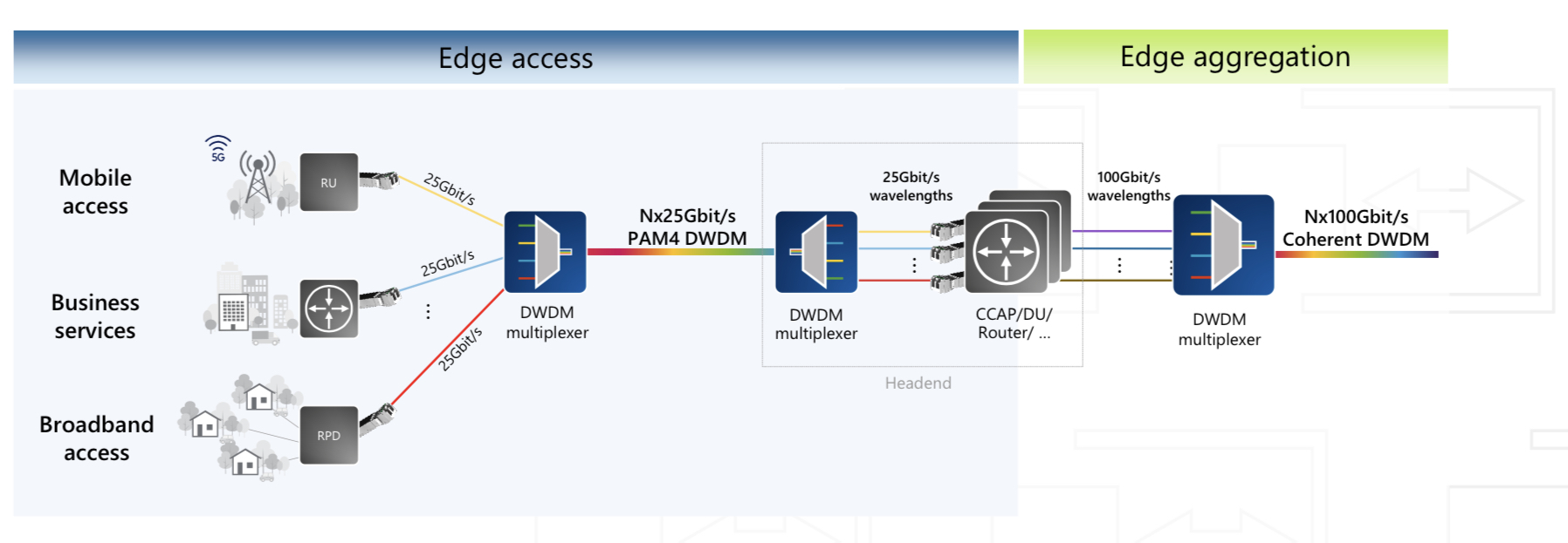
ADVA targets access with its latest pluggable module
- The 25 gigabit-per-second (Gbps) SFP28 is self-tuning and has a reach of 40km
- ADVA’s CEO, Christoph Glingener, in his plenary talk at ECOC 2022 addressed the unpredictable nature of technology adoption.
ADVA has expanded its portfolio of optical modules with an SFP28 for the access market.
The AccessWave25 is a self-tuning dense wavelength division multiplexing (DWDM) pluggable.
The SFP28 is designed to enable communications service providers to straightforwardly upgrade their access networks from 10Gbps to 25Gbps.
ADVA made the announcement just before ECOC 2022.
Features
The SFP28 module links switches and routers to DWDM open-line systems (see diagram below).
The 40km-reach pluggable uses 4-level pulse amplitude modulation (PAM-4) and supports 25 gigabit Ethernet and eCPRI traffic.
The module uses the G.metro self-tuning standard to coordinate with the remote-end transceiver a chosen channel in the C-band, simplifying configuration and removing human error.
The G.metro communication channel also enables remote monitoring of the module.
The SFP28 consumes 3W and works over the extended temperature of -40 to 85oC.
Strategy
ADVA says vertical integration is a critical part of its Optical Engine unit’s strategy.
Saeid Aramideh, ADVA’s Optical Engine’s vice president of business development, says the unit focusses on such technology disciplines as silicon photonics, laser technology and digital signal processing.
The digital signal processing includes aggregation as with ADVA‘s MicroMux module products, PAM-4 used by the AccessWave25, and coherent as with its 100ZR module announced in June.
Advanced packaging is another technology area of interest.
“These are the fundamental innovation areas we focus on,” says Aramideh. “We build our product portfolio based on these platforms.”
ADVA also looks at the market to identify product gaps.
“Not so much every MSA module, but what is happening on the aggregation side,” says Aramideh. “What is it that other people are not paying attention to?”
This is what motivated ADVA’s MicroMux products. The MicroMux module family includes a 10-by-10 gigabit going into 100 gigabits, a 10-by-one gigabit into 10 gigabits, and a four-by-100 gigabit going into 400 gigabits.
“The reality is over 10,000 MicroMux modules are carrying traffic with a top tier-one network provider in Europe,“ says Aramideh. “Not on ADVA equipment but on other network equipment maker, which we haven’t made public.”
For access aggregation, ADVA unveiled at OFC its four-by-10 gigabit MicroMux Edge BiDi with a 40km reach.
“This is for Ethernet, backhaul, and services where fibre is limited and symmetric latency is important,” says Aramideh.
ADVA’s 100ZR module uses a coherent digital signal processor (DSP) developed with Coherent. The 100ZR is a QSFP28 module that dissipates 5W and reaches 300km.
Now, ADVA has added the AccessWave25, a tunable SFP28 that uses direct-detect technology and PAM-4, including ADVA’s IP for distance optimisation.
“The AccessWave25 works on legacy, so if you have a 10-gigabit network, you don’t have to change anything on the physical layer,” he says.
ADVA also looks at metro applications and says it will announce lower-power, smaller form factor coherent designs.
ECOC plenary talk
The CEO of ADVA, Christoph Glingener, gave a plenary talk at ECOC.
Entitled Never say never, Glingener reflected on technology adoption and its timing.
He pointed out how technologies that, at first, seem impractical or too difficult to adopt can subsequently become mainstream. He cited coherent optical communication as one example.
Glingener also discussed how such unpredictability impacts business, citing supply-chain issues, the global pandemic, and sovereignty.
Sovereignty and the influx of government capital for fibre rollout and semiconductors confirm that the optical communications industry is in a good place. But Glingener worries how the industry’s practitioners are ageing and stresses more needs to be done to attract graduates.
Tracing optical communications’ progress, he talked about the 15-year cycles of first direct detect and then fibre amplification. Coherent then followed in 2010.
The industry is thus ripe for breakthrough technology.

Reaching limits
Shannon’s limit means spectral efficiency no longer improves while Moore’s law’s demise continues. Near-term trends are clear, he says, parallelism, whether it is multiple spectrum bands, multiple fibres, or multiple fibre cores. This, in turn, will drive new optical amplifier and wavelength-selective switch designs.
Further optimisation will be needed, integration at the device level and the creation of denser systems. Network automation is also essential and that requires much work.
Glingener also argues for optical bypass rather than electrical packet processing. Large core routers overseeing routing at the IP and optical layer will not aid the greening of the internet.
Next wave
So what is the next technology wave?
Possibilities he cited include hollow-core fibre, photonic computing, and quantum entanglement for communications and the quantum internet.
Will they reach a large scale? Glingener is doubtful.
Whatever the technology proves to be, he said, it is likely already being discussed at ECOC 2022.
If he has a message for the audience, it is to apply their own filter whenever they hear people say, ‘it will never come,’ or ‘it is too difficult.’ Never say never, says Glingener.

ECOC '22 Reflections - Part 2

Gazettabyte is asking industry and academic figures for their thoughts after attending ECOC 2022, held in Basel, Switzerland. In particular, what developments and trends they noted, what they learned, and what, if anything, surprised them.
In Part 2, Broadcom‘s Rajiv Pancholy, optical communications advisor, Chris Cole, LightCouting’s Vladimir Kozlov, Ciena’s Helen Xenos, and Synopsys’ Twan Korthorst share their thoughts.
Rajiv Pancholy, Director of Hyperscale Strategy and Products Optical Systems Division, Broadcom*
The buzz at the show reminded me of 2017 when we were in Gothenburg pre-pandemic, and that felt nice.
Back then, COBO (Consortium for On-Board Optics) was in full swing, the CWDM8 multi-source agreement (MSA) was just announced, and 400-gigabit optical module developments were the priority.
This year, I was pleased to see the show focused on lower power and see co-packaged optics filter into all things ECOC.
Broadcom has been working on integrating a trans-impedance amplifier (TIA) into our CMOS digital signal processor (DSP), and the 400-gigabit module demonstration on the show floor confirmed the power savings integration can offer.
Integration impacts power and cost but it does not stop there. It’s also about what comes after 2nm [CMOS], what happens when you run out of beach-front area, and what happens when the maximum power in your rack is not enough to get all of its bandwidth out.
It is the idea of fewer things and more efficient things that draws everyone to co-packaged optics.
The OIF booth showcased some of the excitement behind this technology that is no longer a proof-of-concept.
Moving away from networking and quoting some of the ideas presented this year at the AI Hardware Summit by Alexis Bjorlin, our industry needs to understand how we will use AI, how we will develop AI, and how we will enable AI.
These were in the deeper levels of discussions at ECOC, where we as an industry need to continue to innovate, disagree, and collaborate.
Chris Cole, Optical Communications Advisor
I don’t have many substantive comments because my ECOC was filled with presentations and meetings, and I missed most of the technical talks and market focus presentations.
It was great to see a full ECOC conference. This is a good sign for OFC.
Here is an observation of what I didn’t see. There were no great new silicon photonics products, despite continued talk about how great it is and the many impressive research and development results.
Silicon photonics remains a technology of the future. Meanwhile, other material systems continue to dominate in their use in products.
Vladimir Kozlov, CEO of LightCounting
I am surprised by the progress made by thin-film lithium niobate technology. There are five suppliers of these devices now: AFR, Fujitsu, Hyperlight, Liobate, and Ori-chip.
Many vendors also showed transceivers with thin-film lithium niobate modulators inside.
Helen Xenos, senior director of portfolio marketing at Ciena
One key area to watch right now is what technology will win for the next Ethernet rates inside the data centre: intensity-modulation direct detection (IMDD) or coherent.
There is a lot of debate and discussion happening, and several sessions were devoted to this topic during the ECOC Market Focus.
Twan Korthorst, Group Director Photonic Solutions at Synopsys.
My main observations are from the exhibition floor; I didn’t attend the technical conference.
ECOC was well attended, better than previous shows in Dublin and Valencia and, of course, much better than Bordeaux (the first in-person ECOC in the Covid era).
I spent three days talking with partners, customers and potential customers, and I am pleased about that.
I didn’t see the same vibe around co-packaged optics as at OFC; not a lot of new things there.
There is a feeling of what will happen with the semiconductor/ datacom industry. Will we get a downturn? How will it look? In other words, I noticed some concerns.
On the other hand, foundries are excited about the prospects for photonic ICs and continue to invest and set ambitious goals.
ECOC 2022 Reflections - Part 1

Gazettabyte is asking industry and academic figures for their thoughts after attending ECOC 2022, held in Basel, Switzerland. In particular, what developments and trends they noted, what they learned, and what, if anything, surprised them.
In Part 1, Infinera’s David Welch, Cignal AI’s Scott Wilkinson, University of Cambridge’s Professor Seb Savory, and Huawei’s Maxim Kuschnerov share their thoughts.
David Welch, Chief Innovation Officer and Founder of Infinera
First, we had great meetings. It was exciting to be back to a live, face-to-face industry event. It was also great to see strong attendance from so many European carriers.
Point-to-multipoint developments were a hot topic in our engagements with service providers and component suppliers. It was also evident in the attendance and excitement at the Open XR Forum Symposium, as well as the vendor demos.
We’re seeing that QSFP-DD ZR+ is a book-ended solution for carriers; interoperability requirements are centred on the CFEC (concatenated or cascaded FEC) market; oFEC (Open FEC) is not being deployed.
Management of pluggables in the optical layer is critical to their network deployment, while network efficiency and power reduction are top of mind.
The definition of ZR and ZR+ needs to be subdivided further into ZR – CFEC, ZR+ – oFEC, and ZR+-HP (high performance), which is a book-ended solution.
Scott T. Wilkinson, Lead Analyst, Optical Components, Cignal AI.
The show was invaluable, given this was our first ECOC since Cignal AI launched its optical components coverage.
Coherent optics announcements from the show did not follow the usual bigger-faster-stronger pattern, as the success of 400ZR has convinced operators and vendors to look at coherent at the edge and inside the data centre.
100ZR for access, the upcoming 800ZR specifications from the OIF, and coherent LR (coherent designed for 2km-10km) will revolutionise how coherent optics are used in networks.
Alongside the coherent announcements were developments from the direct-detect vendors demonstrating or previewing key technologies for 800 Gigabit Ethernet (GbE) and 1.6 Terabit Ethernet (TbE) modules.
800GbE is nearly ready for prime time, awaiting completion of systems based on the newest 112 gigabit-per-second (Gbps) serialiser-deserialiser (serdes) switches. The technology for 224Gbps serdes is just starting to emerge and looks promising for products in late 2024 or 2025.
While there were no unexpected developments at the show, it was great to compare developments across the industry and understand the impact of supply chain issues, operator deployment plans, and any hints of oversupply.
We came away optimistic about continued growth in optical components shipments and revenue into 2023.
Seb Savory, Professor of Optical Fibre Communication, University of Cambridge
My overwhelming sense from ECOC was it was great to be meeting in person again. I must confess I was looking at logistics as much as content with a view to ECOC 2023 in Glasgow where I will be a technical programme committee chair.
Maxim Kuschnerov, Director of the Optical and Quantum Communications Laboratory at Huawei
In the last 12 months, the industry has got more technical clarification regarding next-generation 800ZR and 800LR coherent pluggables.
While 800ZR’s use case seems to be definitely in the ZR+ regime, including 400 gigabit covering metro and long-haul, the case for 800LR is less clear.
Some proponents argue that this is a building block toward 1.6TbE and the path of coherence inside the data centre.
Although intensity-modulation direct detection (IMDD) faces technical barriers to scaling wavelength division multiplexing to 8×200 gigabit, the technological options for beyond 800-gigabit coherent aren’t converging either.
In the mix are 4×400 gigabit, 2×800 gigabit and 1×1.6 terabit, making the question of how low-cost and low-power coherent can scale into data centre applications one of the most interesting technical challenges for the coming years.
Arista continues making a case for a pluggable roadmap through the decade based on 200-gigabit serdes.
With module power envelopes of around 40W at the faceplate, it shows the challenge that the industry is facing and the case co-packaged optics is trying to make.
However, putting all the power into, or next to, the switching chip doesn’t make the cooling problem any less problematic. Here, I wonder if Avicena’s microLED technology could benefit next-generation chip-to-chip or die-to-die interconnects by dropping the high-speed serdes altogether and thus avoiding the huge overhead current input-output (I/O) is placing on data centre networking.
It was great to see the demo of the 200-gigabit PAM-4 externally modulated laser (EML) at Coherent’s booth delivering high-quality eye diagrams. The technology is getting more mature, and next year will receive much exposure in the broader ecosystem.
As for every conference, we have seen the usual presentations on Infinera’s XR Optics. Point-to-multipoint coherent is a great technology looking for a use case, but it is several years too early.
At ECOC’s Market Focus, Dave Welch put up a slide on the XR ecosystem, showing several end users, several system OEMs and a single component vendor – Infinera. I think one can leave it at this for now without further comment.
Ciena's multi-format 400G coherent QSFP-DD pluggable
Ciena showcased a working 400-gigabit Universal coherent pluggable module at the ECOC 2022 conference and exhibition in Basel, Switzerland.
Ciena is using its WaveLogic 5 Nano coherent digital signal processor (DSP) for the Universal QSFP-DD coherent pluggable module.
“We call it universal because it supports many transmission modes – interoperable and high performance; the most in the industry,” says Helen Xenos, senior director of portfolio marketing at Ciena.
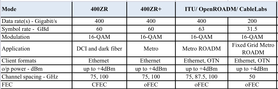
The pluggable has custom extended-performance modes and supports three industry formats: the 400ZR interoperable standard, the 400ZR+ multi-source agreement (MSA), and the OpenROADM MSA. (See tables below).
IP over DWDM
Communications service providers (CSPs) want to add pluggable coherent modules to their IP routers, removing the need for a separate transponder card or box linking the router to the optical line system.
The advent of coherent QSFP-DD pluggables has meant the same form factor can be used for client-side and line-side optics, ensuring efficient use of the router ports.
The CSPs want the coherent QSFP-DD module to have sufficient optical performance to meet their demanding networking requirements. For example, the module’s output signal can pass through the filtering stages of reconfigurable optical add-drop multiplexers (ROADMs) along the optical link.
Optical amplification and filtering
Ciena’s coherent QSFP-DD adds a fibre-based optical amplifier and a tunable optical filter to the coherent photonics and electronic ICs.
The optical amplification enables the high-performance mode and the launching of a 4dBm output signal. In contrast, 400ZR and 400ZR+ have a launch power of -10dBm.
“This is the industry’s highest [QSDP-DD] transmit power,” says Xenos.
The tunable optical filter improves the optical performance of the coherent receiver.
In an optical line system with colourless ROADMs, the Erbium-doped fibre amplifiers (EDFAs) generate out-of-band transmission noise – amplified spontaneous emission (ASE). The noise sources superimpose and become significant, impairing wavelength and system performance dramatically.
The tunable optical filter eliminates this effect and simplifies deployment over any photonics line system. In addition, Ciena says the pluggables can now work alongside high-baud rate transponders in existing ROADM applications.
The QSFP-DD’s tunable optical filter means its optical performance closely matches that of the CFP2-DCO, aiding the two classes of pluggables working together.
Modes of operation
400ZR defines the module’s baseline coherent performance. The OIF developed the 400ZR standard so hyperscalers can link their equipment in two separate data centres up to 120km apart.
The 400ZR specification delivers just enough optical performance to meet the optical link budget. The OIF produced a low-cost, interoperable, pluggable coherent specification.
400ZR supports a single baud rate – 60 gigabaud (GBd), and modulation scheme – dual-polarisation 16-QAM, and carries Ethernet frames.
Google, Meta, Microsoft and Alibaba were all involved in the OIF development, with the 400ZR Implementation Agreement published in early 2020.
400ZR supports two-channel widths: 75GHz and 100GHz, while the forward error correction scheme used is CFEC.
The 400ZR+ MSA enhances the performance by supporting other data rates – 100, 200 and 300 gigabits-per-second (Gbps) – as well as 400Gbps. In addition, it uses several modulation schemes and the enhanced O-FEC error correction scheme that extends reach.
Ciena’s module also meets the OpenROADM MSA, supporting Ethernet and OTN and an enhanced reach at 400Gbps.

Ciena’s Universal module’s extended performance modes up the symbol rate to 65 and 70 gigabaud (GBd) and uses probabilistic constellation shaping (PCS).
PCS maps the bitstream onto the constellation to maximise the data recovery at the coherent receiver, thereby improving overall optical performance. The scheme also allows the fine-tuning of the data rate sent.
At ECOC, Ciena showed the module implementing the high-performance mode at 70GBd and PCS.
ECOC innovation award
The ECOC Exhibition Market Focus Advisory Committee awarded the most innovative product award to Ciena’s WaveLogic 5 Nano 400G Universal QSFP-DD.

Tencent makes its co-packaged optics move

- Tencent is the first hyperscaler to announce it is deploying a co-packaged optics switch chip
- Tencent will use Broadcom’s Humboldt that combines its 25.6-terabit Tomahawk 4 switch chip with four optical engines, each 3.2 terabit-per-second (Tbps)
Part 2: Broadcom’s co-packaged optics
Tencent will use Broadcom’s Tomahawk 4 switch chip co-packaged with optics for its data centres.
“We are now partnered with the hyperscaler to deploy this in a network,” says Manish Mehta, vice president of marketing and operations optical systems division, Broadcom. “This is a huge step for co-packaged optics overall.”
Broadcom demonstrated a working version of a Humboldt switch at OFC earlier this year.
The Chinese hyperscaler will use Broadcom’s 25.6Tbps Tomahawk 4 Humboldt, a hybrid design where half of the chip’s input-output (I/O) is optical and half is the chip’s serialisers-deserialisers (serdes) that connect to pluggable modules on the switch’s front panel.
Four Broadcom 3.2-terabit silicon photonics-based optical engines are co-packaged alongside the Tomahawk 4 chip to implement 12.8Tbps of optical I/O.
Broadcom demonstrated a working version of a Humboldt switch at OFC earlier this year.
Co-packaged optics
Broadcom started its co-packaged optics development work in 2019.
“One of the reasons for our investment in co-packaged optics was that we did see firsthand the ongoing limits of copper interconnect being approached,” says Mehta.
The transmission reach of copper links continues to shrink as the signalling speed has increased from 25 gigabits-per-second (Gbps) non-return to zero (NRZ) to PAM-4 (4-level pulse amplitude modulation) based signalling at 56Gbps, 112Gbps and, in the coming years, 224Gbps. Power consumption is also rising with each speed hike.
Broadcom says data centres now use 1 million optical interconnects, but that much of the connectivity is still copper-based, linking adjacent racks and equipment within the rack.
“Hyperscalers spend ten times more on interconnects than switching silicon,” says Mehta. Given these trends, there needs to be a continual improvement in the power profile, cost and scaled manufacturing of optical interconnect, he says.
In the short term, what is driving interest in co-packaged optics is overcoming the limitations of copper, says Broadcom.
In early 2021, Broadcom detailed at a JP Morgan event its co-packaged optics roadmap. Outlined was the 25.6-terabit Humboldt to be followed by Bailly, a 51.2-terabit all co-packaged optics design using Broadcom’s Tomahawk 5 switch chip which is now sampling.
Humboldt uses DR4 (4×100-gigabit using 4 fibres) whereas the 51.2-terabit Bailly will add multiplexing-demultiplexing and use the FR4 specification (4×100-gigabit wavelengths per fibre).
Technology and partners
Broadcom’s in-house technology includes lasers (VCSELs and EMLs), mixed-signal expertise (trans-impedance amplifiers and drivers), and silicon photonics, as well as its switch chips.
Broadcom uses a remote laser source for its co-packaged optics design. Placing the laser away from the package (the switch chip and optics) means no cooling is needed.
Broadcom is working with 15 partners to enable its co-packaged optics, highlighting the breadth of expertise required and the design complexity.
There are two prominent use cases for the hybrid I/O Humboldt.
One is for top-of-rack switches, where the electrical interfaces support short-reach copper links connecting the servers in a rack, while the optical links connect the top-of-rack box to the next layer of aggregation switching.
The second use is at the aggregation layer, where the electrical I/O connects other switches in the rack while the optical links connect to switch layers above or below the aggregation layer.
“There is a use case for having pluggable ports where you can deploy low-cost direct-attached copper,” says Mehta.
Broadcom says each data centre operator will have their own experience with their manufacturing partners as they deploy co-packaged optics. Tencent has decided to enter the fray with 25.6-terabit switches.
“It is not just Broadcom developing the optical solution; it is also ensuring that our manufacturing partner is ready to scale,” says Mehta.
Ruijie Networks is making the two-rack-unit (2RU) switch platform for Tencent based on Broadcom’s co-packaged optics solution. The co-packaged optics interfaces are routed to 16 MPO connectors while the switch supports 32, 400-gigabit QSFP112 modules.
“It’s always important to have your lead partner [Tencent] for any deployment like this, someone you’re working closely with to get it to market,” says Mehta. “But there is interest from other customers as well.”
Cost and power benefits
Broadcom says co-packaged optics will lower the optical cost-per-bit by 40 per cent while the system (switch platform) power savings will be 30 per cent.
Humboldt more than halves the power compared to using pluggables. Broadcom’s co-packaged optics consumes 7W for each 800-gigabits of bandwidth, whereas an equivalent 800-gigabit optical module consumes 16-18W.
Its second-generation design will embrace 5nm CMOS rather than 7nm and still more than halve the power: an 800-gigabit pluggable will consume 14-15W, whereas it will be 5.5W for the same co-packaged optics bandwidth.
Broadcom will move to CMOS for its second-generation electrical IC; it uses silicon germanium at present.
Power and operational cost savings are a longer-term benefit for data centre operators, says Broadcom. A more immediate concern is the growing challenge of managing the thermal profile when designing switching systems. “The amount of localised heat generation of these components is making systems quite challenging,” says Mehta.
A co-packaged design eliminates pluggables, making system design easier by improving airflow via the front panel and reducing the power required for optical interconnect.
“They’ve been telling us this directly,” says Mehta. “It’s been a pretty good testimonial to the benefits they can see for system design and co-packaged optics.”
Roadmap
At OFC 2022, Broadcom also showed a mock-up of Bailly, a 51.2 terabit switch chip co-packaged with eight 6.4Tbps optical engines.
Broadcom will offer customers a fully co-packaged optics Tomahawk 5 design but has not given a date.
Since Broadcom has consistently delivered a doubling of switch silicon capacity every 24 months, a 102.4-terabit Tomahawk 6 is scheduled to sample in the second half of 2024.
That timescale suggests it will be too early to use 224Gbps serdes being specified by the OIF. Indeed, Mehta believes 112Gbps serdes will have “a very long life”.
That would require the next-generation 102.2Tbps to integrate 1024, 100Gbps serdes on a die. Or, if that proves too technically challenging, then, for the first time, Broadcom’s switching ASIC may no longer be a monolithic die.
Broadcom’s networking group is focused on high-speed serial electrical interfaces. But the company is encouraged by developments such as the open standard UCIe for package interconnect, which looks at slower, wider parallel electrical interfaces to support chiplets. UCIe promises to benefit co-packaged optics.
Broadcom’s view is that it is still early with many of these design challenges.
“Our goal is to understand when we need to be ready and when we need to be launching our silicon on the optical side,” says Mehta. “That’s something we are working towards; it’s still not clear yet.”

The significance of 6G
Henning Schulzrinne is known for speaking his mind.
A professor at the Department of Computer Science and the Department of Electrical Engineering at Columbia University, he previously expressed concern regarding what he saw as excessive hype surrounding 5G.
More recently, he has written about 6G, placing the emerging wireless standard in the broader context of societal needs.
“Research, particularly academic research, should be driven by the urgent needs of society, not just supplying patent-protected ‘moats’ against the competition, whether between companies or nations,” he wrote in an introduction to the book, Shaping Future 6G Networks.
Schulzrinne stresses he is not working on 6G standards but has taken part in an early 6G flagship project at the University of Oulu, Finland.
“My expertise is not on the radio; it is system architecture,” he says. “We have a lot of interest in my research group on issues such as automation and authentication, not specifically to 6G but to networks.”
Wireless generations
Every decade, work starts on a new-generation cellular wireless standard.
In the past, each generation represented a significant change. “You started with a clean slate, the [2G] digital system had very little in common with the analogue system that preceded it, and 3G was a different beast to 2G,” says Schulzrinne. “It made sense to call each a generational change.”
Now, release cycles are shorter, and there are what Schulzrinne calls ‘arbitrary markers’, such as when the 3GPP standards body issues a new Release or when the standard is suddenly called 4G.
Now, the notion of a new generation has become forced.
There is no solely-5G handset since it also supports earlier-generation standards. Supporting multiple generations is common in wireless; Wi-Fi devices may fall back to earlier standards for a connection.
He views 6G as more of an exercise for stakeholders such as consumers, policymakers and investors. “Putting a label on it helps to crystallise efforts, primarily outside the industry,” he says.
5G wireless
Schulzrinne notes how each 5G deployment still generates a press release: “You don’t see that for other things where people buy stuff.”
He also has doubts about some of the stated promises of 5G, such as its use to transform other industries.
“The question I don’t get a good answer to is, with the digitisation of industry, does it involve a plant that had no network at all, or a minimal networking capability and they wanted to create a network?” says Schulzrinne. “Why do they choose 5G; what value creation does it give?”
In US factories, robotics is usually fixed rather than mobile. Beating Ethernet on cost is also hard, he says, and factories can be hostile environments for radio.
In China, the three main operators are showing growth in service revenues from new ‘industrial digitalisation’ services. But then China is an advanced, large-scale manufacturer.
“I’m trying to have an open mind,” says Schulzrinne. “But where is that coming from, and what revenue is there outside of China?”
What 5G does bring is the opening up of radio spectrum, not just millimetre wave but also between 2GHz and 6GHz. 5G has also moved away from classical software to virtual network functions and cloud-based building blocks.
“This architectural transformation behind the scenes, which is hard to write flashy stories about, seems much more interesting,” says Schulzrinne.
Smaller carriers, and those outside the leading industrial countries, can now outsource parts of their operation to other parties; all that is needed is a cloud provider and software.

6G: uses and metrics
It is too early to summarise 6G.
5G’s main story is its three performance pillars: supporting many more devices, a tenfold hike in data speeds, and ultra-low latency.
For 6G, two stories are emerging.
One is consumer, involving the Metaverse, although Schulzrinne remains sceptical about the degree that is a motivating factor for 6G.
The second is technology related, and there are two parts here. One is AI and machine learning, although it is not clear as yet what role the technology will play with 6G.
The second, potentially transformational, is using 6G networks for sensing. For example, the position, movement and actions of entities in the field of view, adding sensing alongside the network’s communication capabilities.
“It’s almost like building a radar; it’s not the same technology, but it’s similar,” says Schulzrinne. Such sensing could be used outdoors and at home as a game controller or for motion detection.
6G will improve the critical performance metrics of 5G, but Schulzrinne believes the more meaningful metrics are cost-per-bit delivered and cost-per-base station-month.
Cost-per-bit is a crucial metric if cellular wireless is to replace Wi-Fi or Ethernet networks in the home and enterprise.
The average household data usage in the US is 400 gigabytes a month, 10x more than the heaviest mobile user.
It is also why Wi-Fi is used for data offload, given that fixed-line offers a cheaper solution than cellular with its base station and mobile backhaul costs. And this is before new data-intensive applications emerge, such as augmented and virtual reality headsets.
6G’s focus should be to reduce base station and backhaul costs.
“If you want to scale up the bits-per-dollar, its going to be a big challenge making that work,” he says.
Calibrating expectations
There will be a mismatch between 6G’s ambition and the likely outcome, he says.
A story told by the telcos is that they want to be the providers of higher-level services, not big data pipes. But this is misguided, says Schulzrinne. Instead, the telcos should aspire to be utilities.
“Many electric utilities, water utilities, don’t grow in double-digit percentages every year, and nobody expects them to, and that’s fine,” says Schulzrinne. “They have an expertise and a set of skills that are necessary and helpful from a societal perspective.”
Their metrics are reliability and cost-effectiveness.
He views 6G as a promising technology upgrade for the operators.
“What I want is fast and cheap, and I rely on the carrier to use modern technology to do that, “he says.
Comparing telcos to electric and water utilities can be taken too far, he says, but what the best of them share is that they provide vital input with changing technology to decrease prices and increase reliability.
They also share facing new challenges like cybersecurity.
“That is their job; it’s not other things,” says Schulzrinne.
Professor Schulzrinne and his research team developed the Session Initiation Protocol (SIP), the Real-Time Transport Protocol (RTP), and other multimedia signalling and support protocols.
Schulzrinne has been an advisor to the US Federal Communications Commission (FCC) and served as FCC Chief Technologist on public safety. He also served as a Technology Fellow in the office of Senator Ron Wyden, addressing data protection.

A career in technology market analysis
John Lively reflects on a 30-year career.
It was a typical workday in 1989, sitting through a meeting announcing the restructuring of Corning’s planar coupler business.
The speaker’s final words were, “Lively, you’ll be doing forecasting.” It changed my life and set my career path for the next 30-plus years.
No one grows up with a desire to be a market analyst. Indeed, I didn’t ask for the job. What made it possible was an IBM PC and LOTUS 1-2-3 in my marine biology lab in the early 1980s (a story for another time).
After a stop at MIT for an MBA, this led to a job in Corning’s fledgling PC support team in 1985. Then it was Corning’s optical fibre business cost-modelling fibre-to-the-home networks on a PC, working with Bellcore and General Instrument engineers. From there, it was to forecast market demand for planar couplers in the FTTH market.
In the following decade, I had various market forecasting roles within Corning’s optical fibre and photonics businesses.
Each time I tried to put forecasting behind me by taking a marketing or product management job, management said they needed me to return to forecasting due to some crisis or another (thank you, Bernie Ebbers).
In 1999, I had an epiphany. If Corning thinks I’m better at forecasting than anything else, perhaps I should become a professional forecaster in a company whose product is forecasts.
Just then, through fate or coincidence, I received a call from fellow MIT alum Dana Cooperson who said her firm, RHK, was desperate for people and did I know anyone who might be interested?
For the uninitiated, that’s code for ‘would you be interested in joining us?’.
I joined just in time to enjoy the remaining months of the boom, followed by a bust in 2001. But all the while learning to be a market analyst in a new context. While at Corning, I had been both a producer and procurer of market research. At RHK, I was strictly a producer.
More importantly, there was a direct link between my words and spreadsheets and money coming in. It was exhilarating.
Working remotely
Thanks to the newly deployed cable modem/ HFC technology that I had been cost-modelling a decade earlier, I was working from home.
I have worked from home ever since, and I can say that remote working does work well for some people and jobs.
Some lessons I’ve learned include:
- Working from home works best if the entire firm, not just a few people, are doing it.
- Home working doesn’t mean you can’t travel, pandemics notwithstanding.
- Home workers need to have clear deliverables that they can be judged against. Give them responsibility for something tangible, with an unambiguous deadline.
- Requiring time-tracking sheets or online monitoring of home workers is insulting and demotivating.
- Companies must support home workers by investing in quality internet services and conferencing software/ equipment on both sides of the link
Required skills
By joining RHK, I had moved from a Fortune 500 company to one of 100 employees. Over the next two decades, I would move between large and small companies. I prefer small companies because it’s clear who contributes to their success and who doesn’t. Poor performers have nowhere to hide in a company of six people.
After more than 30 years in the market research arena, I have views on the role of a market analyst and the talents necessary to be a good one.
The goal of market analysis is to find information, analyse it, draw conclusions, then package and communicate it.
Doing market research is like assembling a jigsaw puzzle, from which several pieces are missing. Or, like a chef who must create a healthy, enjoyable meal from an assortment of good and bad raw ingredients.
A technology market analyst should be intellectually curious, have a solid background in sciences and technology, and have broad industry knowledge, i.e., understand the jargon, the tech, and the companies.
The analyst also needs to write concisely and quickly, is fluent in Excel, PowerPoint, and Word, is a great communicator and is approachable, likeable, and outgoing.
Of course, finding all the requisite skills in one person is rare, and larger companies commonly divide duties into specialities like data collection, analysis, and communication.
In small companies, this may not be overt but happens to a degree just the same.
Most importantly, a market analyst must be comfortable with uncertainty.
One never has all the pieces, and you must be OK filling in missing data points via extrapolation, intuition, historical parallels, or other means. And be comfortable admitting your mistakes and adjusting your findings when new data surfaces.
I believe this is why those with a scientific background are better suited to market research than engineers. Scientists are taught scepticism and revision as a way of life, while engineers seek the certainty of the ‘right’ answer.
Periods of note
Throughout my career, I’ve lived through interesting times.
Starting in 1985, it was the introduction of the first PCs into Corning and establishing their first email system, electronic newsletter, word processing, and expert-learning systems.
Then, in the mid-1990s working in the early days of amplified DWDM systems and when the EDFA business doubled its output yearly.
Then came the Internet bubble and optical industry boom/bust of 1999-2001, when dozens of companies were founded by a couple of PhDs with a PowerPoint presentation. At one point in 2000, my optical components practice at RHK had over 100 subscribing companies.
It was weird living through an episode that we knew would someday be written about, like the Dutch tulip mania of 1634.
More recently, and I believe, with a more positive outcome, it is/ has been fascinating to watch companies like Alphabet, Amazon, and Meta utilise a globally connected internet to become the first truly global communications, media, and retail companies.
Moreover, these companies transcend national, cultural, and language boundaries, connecting a billion or more users. And in the process, inventing hyperscale data centres, which in turn allow hundreds and thousands of other companies to ‘cloudify’ as well, extending their global reach.
Of all the innovations and changes taking place today, this is one I will continue to follow with wonder and amazement.
The promise of these companies is so great that I’m hopeful they will become beacons of positive change around the world in the 21st century.
Innovation has been breathtaking in optics. For example, coherent transport, the far-out science stuff of technical talks at my first OFC in 1988, is in commercial use.
We blithely speak of optical transceivers capable of Terabit-per-second speeds without stopping to think how amazing it is that anything, anywhere, could be made to turn off and on again, one TRILLION times a second!
It simply defies human understanding, and yet we make it easy.
A view of now
Today, it’s easy to be convinced that things are falling apart, between Russia’s war against Ukraine, COVID, economic turmoil, screwed-up supply chains, and populist politicians.
But I take solace that I’ve seen things like this before and lived through them. As a child, scenes of the Vietnam war were on the news every evening. But finally, there was peace in Vietnam.
In the 1970s, we had an oil embargo and sky-high gas prices. It also ended.
In the 1980s, inflation ran hot, pushing my student loan interest rate to 13%. But I paid it off, and rates came down.
AIDS struck fear and stoked prejudice for years, claiming my aunt and uncle before scientists uncovered its secrets and developed effective treatments.
So it will be with COVID. History shows that humans tire of strife and disease and will work to conquer our worst problems eventually.
Surprises
Two things come to mind regarding industry surprises over the last 30 years.
One is that optical technology keeps advancing. Despite how challenging each new generation seems, bit by bit and idea by idea, the industry collectively comes up with a solution, and the subsequent speed hike is commercialised.
Another is how people find ways to use it no matter how much bandwidth is created. RHK founder, John Ryan, was fond of telling us, “Bandwidth is like cupboard space; it’s never left empty for long.”
Another surprising thing is how long the interpersonal bonds formed at RHK have lasted.
Though it was just a flash in time, many of those who were there in 2000 remain connected as friends and colleagues more than 20 years later.
Several such alumni work at LightCounting now.
Climate Change
While doing all this, looking backwards and reflecting on change, I couldn’t help dwelling on another major problem we face today: climate change.
Forestalling climate change is the one thing I believe where humans are failing. But unfortunately, the causes are so rooted in our global socio-economic systems that citizens and governments are not capable of inflicting the necessary sacrifices on themselves.
I fear the worst-case scenarios are coming soon, with shifting temperature zones and rising seas. In response, many people, plants, and animals will migrate, following favourable conditions north or south or inland as the case may be, significantly increasing competition for resources of all kinds.
I also fear authoritarian governments may prove more effective at providing protection for some, and avoiding utter chaos, than our precious but fragile democracies.
A role for tech giants
I think the internet and companies with global reach can play a role in combatting the worst impacts of climate change.
Some of the hyperscalers, telecom operators, and equipment companies have been leaders in reducing carbon emissions.
I hope the interconnectedness and massive computing power of companies like Meta and Alphabet can be used to solve these large-scale problems.
My last thought is the realisation that when I eventually ease into retirement and cut back on travel, I may never get a chance to personally thank all the friends and colleagues I have made along the way.
People who have assisted my career, believed in me, educated me, and made me think differently, smile, and laugh.
So, just in case, I’ll say it here – thank you one and all – you made a difference to me.
It’s also been fun.

Broadcom samples the first 51.2-terabit switch chip
- Broadcom’s Tomahawk 5 marks the era of the 51.2-terabit switch chip
- The 5nm CMOS device consumes less than 500W
- The Tomahawk 5 uses 512, 100-gigabit PAM-4 (4-level pulse amplitude modulation) serdes (serialisers-deserialisers)
- Broadcom will offer a co-packaged version combining the chip with eight 6.4 terabit-per-second (Tbps) optical engines
Part 1: Broadcom’s Tomahawk 5
Broadcom is sampling the world’s first 51.2-terabit switch chip.
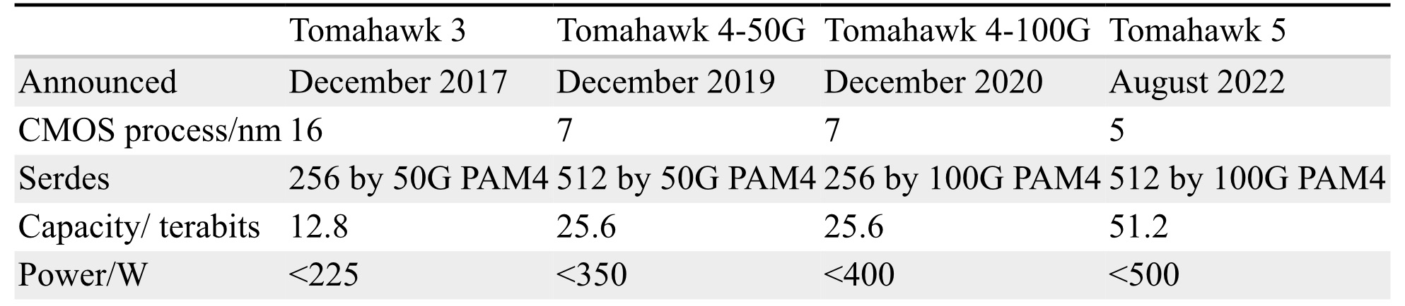
With the Tomahawk 5, Broadcom continues to double switch silicon capacity every 24 months; Broadcom launched the first 3.2-terabit Tomahawk was launched in September 2014.
“Broadcom is once again first to market at 51.2Tbps,” says Bob Wheeler, principal analyst at Wheeler’s Network. “It continues to execute, while competitors have struggled to deliver multiple generations in a timely manner.”
Tomahawk family
Hyperscalers use the Tomahawk switch chip family in their data centres.
Broadcom launched the 25.6-terabit Tomahawk 4 in December 2019. The chip uses 512 serdes, but these are 50-gigabit PAM-4. At the time, 50-gigabit PAM-4 matched the optical modules’ 8-channel input-output (I/O).
Certain hyperscalers wanted to wait for 400-gigabit optical modules using four 100-gigabit PAM-4 electrical channels, so, in late 2020, Broadcom launched the Tomahawk4-100G switch chip, which employs 256, 100-gigabit PAM-4 serdes.
Tomahawk 5 doubles the 100-gigabit PAM-4 serdes to 512. However, given that 200-gigabit electrical interfaces are several years off, Broadcom is unlikely to launch a second-generation Tomahawk 5 with 256, 200-gigabit PAM-4 serdes.
Switch ICs
Broadcom has three switch chip families: Trident, Jericho and the Tomahawk.
The three switch chip families are needed since no one switch chip architecture can meet all the markets’ requirements.
With its programable pipeline, Trident targets enterprises, while Jericho targets service providers.
According to Peter Del Vecchio, Broadcom’s product manager for the Tomahawk and Trident lines, there is some crossover. For example, certain hyperscalers favour the Trident’s programmable pipeline for their top-of-rack switches, which interface to the higher-capacity Tomahawk switches chips at the aggregation layer.
Monolithic design
The Tomahawk 5 continues Broadcom’s approach of using a monolithic die design.
“It [the Tomahawk5] is not reticule-limited, and going to [the smaller] 5nm [CMOS process] helps,” says Del Vecchio.
The alternative approach – a die and chiplets – adds overall latency and consumes more power, given the die and chiplets must be interfaced. Power consumption and signal delay also rise whether a high-speed serial or a slower, wider parallel bus is used to interface the two.
Equally, such a disaggregated design requires an interposer on which the two die types sit, adding cost.
Chip features
Broadcom says the capacity of its switch chips has increased 80x in the last 12 years; in 2010, Broadcom launched the 640-gigabit Trident.
Broadcom has also improved energy efficiency by 20x during the same period.
“Delivering less than 1W per 100Gbps is pretty astounding given the diminishing benefits of moving from a 7nm to a 5nm process technology,” says Wheeler.
“In general, we have achieved a 30 per cent plus power savings between Tomahawk generations in terms of Watts-per-gigabit,” says Del Vecchio.

These power savings are not just from advances in CMOS process technology but also architectural improvements, custom physical IP designed for switch silicon and physical design expertise.
“We create six to eight switch chips every year, so we’ve gotten very good at optimising for power,” says Del Vecchio
The latest switch IC also adds features to support artificial intelligence (AI)/ machine learning, an increasingly important hyperscaler workload.
AI/ machine learning traffic flows have a small number of massive ‘elephant’ flows alongside ‘mice’ flows. The switch chip adds elephant flow load balancing to tackle congestion that can arise when the two flow classes mix.
“The problem with AI workloads is that the flows are relatively static so that traditional hash-based load balancing will send them over the same links,” says Wheeler. “Broadcom has added dynamic balancing that accounts for link utilisation to distribute better these elephant flows.”
The Tomahawk 5 also provides more telemetry information so data centre operators can better see and tackle overall traffic congestion.
The chip has added virtualisation support, including improved security of workloads in a massively shared infrastructure.
Del Vecchio says that with emerging 800-gigabit optical modules and 1.6 terabit ones on the horizon, the Tomahawk 5 is designed to handle multiples of 400 Gigabit Ethernet (GbE) and will support 800-gigabit optical modules.
The chip’s 100-gigabit physical layer interfaces are combined to form 800 gigabit (8 by 100 gigabit), which is fed to the MAC, packet processing pipeline and the Memory Management Unit to create a logical 800-gigabit port. “After the MAC, it’s one flow, not at 400 gigabits but now at 800 gigabits,” says Del Vecchio.
Market research firm, Dell’Oro, says that 400GbE accounts for 15 per cent of port revenues and that by 2026 it will rise to 57 per cent.
Broadcom also cites independent lab test data showing that its support for RDMA over Converged Ethernet (RoCE) matches the performance of Infiniband.
“We’re attempting to correct the misconception promoted by competition that Infiniband is needed to provide good performance for AI/ machine learning workloads,” says Del Vecchio. The tests used previous generation silicon, not the Tomahawk 5.
“We’re saying this now since machine learning workloads are becoming increasingly common in hyperscale data centres,” says Del Vecchio.
As for the chip’s serdes, they can drive 4m of direct attached copper cabling, with sufficient reach to connect equipment within a rack or between two adjacent racks.
Software support
Broadcom offers a software development kit (SDK) to create applications. The same SDK is common to all three of its switch chip families.
Broadcom also supports the Switch Abstraction Interface (SAI). This standards-based programming interface sits on top of the SDK, allowing the programming of switches independent of the silicon provider.
Broadcom says some customers prefer to use its custom SDK. It can take time for changes to filter up, and a customer may want something undertaken that Broadcom can develop quickly using its SDK.
System benefits
Doubling the switch chip’s capacity every 24 months delivers system benefits.That is because implementing a 51.2-terabit switch using the current generation Tomahawk 4 requires six such devices.

Now a single 2-rack-unit (2RU) Tomahawk 5 switch chip can support 64 by 800-gigabit, 128 by 400-gigabit and 256 by 200-gigabit modules.
These switch boxes are air-cooled, says Broadcom.
Co-packaged optics
In early 2021 at a J.P Morgan analyst event, Broadcom revealed its co-packaged optics roadmap that highlighted Humboldt, a 25.6-terabit switch chip co-packaged with optics, and Bailly, a 51.2-terabit fully co-packaged optics design.
At OFC 2022, Broadcom demonstrated a 25.6Tbps switch that sent half of the traffic using optical engines.
Also shown was a mock-up of Bailly, a 51.2 terabit switch chip co-packaged with eight optical engines, each at 6.4Tbps.
Broadcom will offer customers a fully co-packaged optics Tomahawk 5 design but has not yet given a date.
Broadcom can also support a customer if they want tailored connectivity with, say, 3/4 of the Tomahawk 5 interfaces using optical engines and the remainder using electrical interfaces to front panel optics.