
Ciena's Tom Mock reflects on a career in telecom
Working for one technology company for so long may be uncommon, says Mock, but not at Ciena: the CTO has clocked 20 years while the CEO boasts 15 years.
 Tom Mock: “I’m about ready to go do something else.”
Mock studied electrical engineering and was at Scientific Atlanta running a product development group before joining Ciena where he crossed over from engineering to marketing. “I’ve been in telecom pretty much my entire career, 35 years worth of telecom,” says Mock. “I’m about ready to go do something else.”
A work colleague says that if there is one word that describes Mock, it is decency: “He has been a key role model of the ‘do the right thing’ culture at Ciena.”
Mock joined Ciena days before the company went public in 1997. He experienced the optical bubble of 1999-2000 and the bust that followed, and just when he thought the company had put that ‘nuclear winter’ behind it, Ciena endured the 2008 global financial crisis.
Now he leaves Ciena as senior vice president of corporate communications. A role, he says, that involves communicating the company's value proposition to the investment community and media, while helping Ciena’s sales staff communicate the company’s brand. The role also involves explaining the significance of the company’s technology: “It is great we can do 16-QAM [quadrature amplitude modulation] on optical, but why is it important?"
When Mock joined Ciena, optical technology in the form of dense wavelength-division multiplexing (DWDM) was starting to be deployed. “You could go to a service provider and say, look, I can increase the capacity of your network by a factor of 16 just by swapping out the bits at the end of your fibre route,” he says.
I remember sitting at my desk looking at stock prices and market capitalisations and realising that a start-up called Corvis ... had a market capitalisation larger than Ford Motor Company
The optical bubble quickly followed. The internet was beginning to change the world, and large enterprises were taking advantage of communication services in new ways. And with it came the inflated expectation that bandwidth demand would grow through the roof. As a result, optical communications became the hottest technology around.
"I remember sitting at my desk looking at stock prices and market capitalisations and realising that a start-up called Corvis, a competitor of ours started by one of the guys that founded Ciena, Dave Huber, had a market capitalisation larger than Ford Motor Company,” says Mock. Ford was the second largest auto manufacturer in the world at the time.
Yet despite all the expected demand for - and speculation in - bandwidth, conversations with Ciena’s customers revealed that their networks were lightly loaded. The inevitable shake-out, once it came, was brutal, particularly among equipment makers. In the end, all that capacity placed in the network was needed, but only from 2006 as the cloud began to emerge and enterprises started making greater use of computing.
“The one positive that came out of the bubble was that a lot of key technologies that enabled things that happened in the late 2000s were developed in that time,” says Mock.
Ciena made several acquisitions during the optical boom, and has done so since; some successful, others less so. Mock says that with most of the good ones, the technology and the market didn't overlap much with Ciena’s.
Speculation didn't work well for the industry in terms of building infrastructure, and it probably doesn't work well in terms of acquisitions.
One acquisition was Cyras Systems for $2.6 billion in 2000, a company developing 10 Gigabit multi-service provisioning platforms and add/ drop multiplexers. But so was Ciena. “That was one example that didn't work so well but if I look at the one that is going the best - Nortel MEN - that was a place where we didn't have as much technology and market overlap,” he says. That makes streamlining products easier and less disruptive for customers.
“The other thing that is important in a good acquisition is a very good understanding of what the end objective is,” he says. “Speculation didn't work well for the industry in terms of building infrastructure, and it probably doesn't work well in terms of acquisitions.”
Making sure the company cultures fit is also key. “In any of these technology acquisitions, it is not just about buying products and markets, it is about buying the capabilities of a workforce,” says Mock. It is important that the new workforce remains productive, and the way that of done is to make sure the staff feel an important part of the company, he says.
Mock highlights two periods that he found most satisfying at Ciena. One was 2006-2008 before the global economic crisis. Ciena was back of a sound financial footing and was making good money. “There was a similar feeling a year to 18 months after the Nortel acquisition” he says. “The integration had been successful, the people were all pointing in the same direction, and employee morale was pretty high.”
You hear about white boxes in the data centre, there are areas in the network where that is going to happen.
What Mock is most proud of in his time at Ciena is the company’s standing. “We do a perception study with our customers every year to 18 months and one of things that comes back is that people really trust the company,” he says. “Our customers feel like we have their best interest at heart, and that is something we have worked very hard to do; it is also the sort of thing you don't get easily.”
Now the industry is going through a period of change, says Mock. If the last 10-15 years can be viewed as a period of incremental change, people are now thinking about how networks are built and used in new ways. It is about shifting to a model that is more in tune with on-demand needs of users, he says: “That kind of shift typically creates a lot of opportunity.” Networks are becoming more important because people are accessing resources in different places and the networks need to be more responsive.
For Ciena it has meant investing in software as more things come under software control. The benefits include network automation and reduced costs for the operators, but it also brings risk. “There are parts of the infrastructure that are likely to become commoditised,” says Mock. “You hear about white boxes in the data centre, there are areas in the network where that is going to happen.”
We both came from small-town, working-class families. Over the years we have probably been more successful that we ever thought we would be, but a lot of that is due to people helping us along the way.
If this is a notable period, why exit now? “It’s a good time for me,” he says. “And there were some things that my wife and I wanted to start looking at.” Mock’s wife retired two years ago and both are keen to give something back.
“We both came from small-town, working-class families,” he says. “Over the years we have probably been more successful that we ever thought we would be, but a lot of that is due to people helping us along the way.”
Mock and his wife were their families’ first generation that got a good professional education. “One of the things that we have taken on board is helping others gain that same sort of opportunity,” he says.
“I’m excited for Tom but will miss having him around,” says his colleague. “Hopefully, in his next phase, he will make the rest of the world a little more decent as well.”
OIF shows 56G electrical interfaces & CFP2-ACO
 “The most important thing for everyone is power consumption on the line card”
The OIF - an industry organisation comprising communications service providers, internet content providers, system vendors and component companies - is developing the next common electrical interface (CEI) specifications. The OIF is also continuing to advance fixed and pluggable optical module specifications for coherent transmission including the pluggable CFP2 (CFP2-ACO).
“These are major milestones that the [demonstration] efforts are even taking place,” says Nathan Tracy, a technologist at TE Connectivity and the OIF technical committee chair.
Tracy stresses that the CEI-56G specifications and the CFP2-ACO remain works in progress. “They are not completed documents, and what the demonstrations are not showing are compliance and interoperability,” he says.
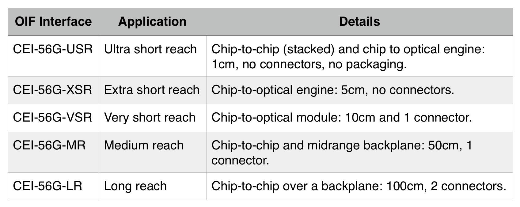
Five CEI-56G specifications are under development, such as platform backplanes and links between a chip and an optical engine on a line card (see Table below).
Moving from the current 28 Gig electrical interface specifications to 56 Gig promises to double the interface capacity and cut electrical interface widths by half. “If we were going to do 400 Gigabit with 25 Gig channels, we would need 16 channels,” says Tracy. “If we can do 50 Gig, we can get it down to eight channels.” Such a development will enable chassis to carry more traffic and help address the continual demand for more bandwidth, he says.
But doubling the data rate is challenging. “As we double the rate, the electrical loss or attenuation of the signal travelling across a printed circuit board is significantly impacted,” says Tracy. “So now our reaches have to get a lot shorter, or the silicon that sends and receives has to improve to significant higher levels.”
One of the biggest challenges in system design is thermal management
Moreover, chip designers must ensure that the power consumption of their silicon do not rise. “We have to be careful as to what the market will tolerate, as one of the biggest challenges in system design is thermal management,” says Tracy. “We can’t just do what it takes to get to 56 Gigabit.”
To this aim, the OIF is pursuing two parallel tracks: using 56 Gigabit non-return-to-zero (NRZ) signalling and 4-level pulse amplitude modulation (PAM-4) which encodes two bits per symbol such that a 28 Gbaud signalling rate can be used. The 56 Gig NRZ uses simpler signalling but must deal with the higher associated loss, while PAM-4 does not suffer the same loss as it is similar to existing CEI-28 channels used today but requires a more complex design.
“Some [of the five CEI-56G specifications] use NRZ, some PAM-4 and some both,” says Tracy. The OIF will not say when it will complete the CEI-56G specifications. However, the projects are making similar progress while the OIF is increasing its interactions with other industry standards groups to shorten the overall timeline.
 Source: OIF, Gazettabyte
Two of the CEI-56G specifications cover much shorter distances: the Extra Short Reach (XSR) and Ultra Short Reach (USR). According to the OIF, in the past it was unclear that the industry would benefit from interoperability for such short reaches.
“What is different at 56 Gig is that architectures are fundamentally being changed: higher data rates, industry demand for higher levels of performance, and changing fabrication technologies,” says Tracy. Such fabrication technologies include 3D packaging and multi-chip modules (MCMs) where silicon dies from different chip vendors may be connected within the module.
The XSR interface is designed to enable higher aggregate bandwidth on a line card which is becoming limited by the number of pluggable modules that can be fitted on the platform’s face plate. Density can be increased by using mid-board optics (an optical engine) placed closer to a chip. Here, fibre from the optical engine is fed to the front plate increasing the overall interface capacity.
The USR interface is to support stackable ICs and MCMs.
All are coming together in this pre-competitive stage to define the specifications, yet, at the same time, we are all fierce competitors
“The most important thing for everyone is power consumption on the line card,” says Tracy. “If you define these very short reach interfaces in such a way that these chips do not need as much power, then we have helped to enable the next generation of line card.”
The live demonstrations at OFC include a CEI-56G-VSR-NRZ channel, a CEI-56G-VSR-PAM QSFP compliance board, CEI-56G-MR/LR-PAM and CEI-56G-MR/LR-NRZ backplanes, and a CEI-56G-MR-NRZ passive copper cable.
The demonstrations reflects what OIF members are willing to show, as some companies prefer to keep their work private. “All are coming together in this pre-competitive stage to define the specifications, yet, at the same time, we are all fierce competitors,” says Tracy.
CFP2-ACO
Also on display is working CFP2 analogue coherent optics (CFP2-ACO). The significance of coherent optics in a pluggable CFP2 is the promise of higher-density line cards. The CFP is a much bigger module and at most four can be fitted on a line card, while with the smaller CFP2, with its lower power consumption, up to eight modules are possible.
Using the CFP2-ACO, the coherent DSP-ASIC is external to the CFP2 module. Much work has been done to ensure that the electrical interface can support the analogue signalling between the CFP2 optics and the on-board DSP-ASIC, says Tracy.
At OFC, several companies have unveiled their CFP2-ACO products including Finisar, Fujitsu Optical Components, Oclaro and NEC, while Clariphy has announced a single-board reference design that includes its CL20010 DSP-ASIC and a CFP2-ACO slot.
MultiPhy readies 100 Gigabit serial direct-detection chip
MultiPhy is developing a chip that will support serial 100 Gigabit-per-second (Gbps) transmission using 25 Gig optical components. The device will enable short reach links within the data centre and up to 80km point-to-point links for data centre interconnect. The fabless chip company expects to have first samples of the chip, dubbed FlexPhy, by year-end.
 Figure 1: A block diagram of the 100 Gig serial FlexPhy. The transmitter output is an electrical signal that is fed to the optics. Equally, the input to the receive path is an electrical signal generated by the receiver optics. Source: Gazettabyte
The FlexPhy IC comprises multiplexing and demultiplexing functions as well as a receiver digital signal processor (DSP). The IC's transmitter path has a CAUI-4 (4x28 Gig) interface, a 4:1 multiplexer and four-level pulse amplitude modulation (PAM-4) that encodes two bits per symbol. The resulting chip output is a 50 Gbaud signal used to drive a laser to produce the 100 Gbps output stream.
"The input/output doesn't toggle at 100 Gig, it toggles at 50 Gig," says Neal Neslusan, vice president of sales and marketing at MultiPhy. "But 50 Gig PAM-4 is actually 100 Gigabit-per-second."
The IC's receiver portion will use digital signal processing to recover and decode the PAM-4 signals, and demultiplex the data into four 28 Gbps electrical streams. The FlexPhy IC will fit within a QSFP28 pluggable module.
As with MultiPhy's first-generation chipset, the optics are overdriven. With the MP1101Q 4x28 Gig multiplexer and MP1100Q four-channel receiver, 10 Gig optics are used to achieve four 28 Gig lanes, while with the FlexPhy, a 25 Gig laser is used. "Using a 25 GigaHertz laser and double-driving it to 50 GigaHertz induces some noise but the receiver DSP cleans it up," says Neslusan.
The use of PAM-4 incurs an optical signal-to-noise ratio (OSNR) penalty compared to non-return-to-zero (NRZ) signalling used for MultiPhy's first-generation direct-detection chipset. But PAM-4 has a greater spectral density; the 100 Gbps signal fits within a 50 GHz channel, resulting in 80 wavelengths in the C-band. This equates to 8 terabits of capacity to connect data centres up to 80 km apart.
Within the data centre, MultiPhy’s physical layer IC will enable 100 Gbps serial interfaces. The design could also enable 400 Gig links over distances of 500 m, 2 km and 10 km, by using four FlexPhys, four transmitter optical sub-assemblies (TOSAs) and four receiver optical sub-assemblies (ROSAs).
Meanwhile, MultiPhy's existing direct-detection chipset has been adopted by multiple customers. These include two optical module makers – Oplink and a Chinese vendor – and a major Chinese telecom system vendor that is using the chipset for a product coming to market now.
Cyan's stackable optical rack for data centre interconnent

"The drivers for these [data centre] guys every day of the week is lowest cost-per-gigabit"
Joe Cumello
The amount of traffic moved between data centres can be huge. According to ACG Research, certain cloud-based applications shared between data centres can require between 40 to 500 terabits of capacity. This could be to link adjacent data centre buildings to appear as one large logical one, or connect data centres across a metro, 20 km to 200 km apart. For data centres separated across greater distances, traditional long-haul links are typically sufficient.
Cyan says it developed the N-series platform following conversations conducted with internet content providers over the last two years. "We realised that the white box movement would make its way into the data centre interconnect space," says Cumello.
White box servers and white box switches, manufactured by original design manufacturers (ODMs), are already being used in the data centre due to their lower cost. Cyan is using a similar approach for its N-Series, using commercial-off-the-shelf hardware and open software.
"The drivers for these [data centre] guys every day of the week is lowest cost-per-gigabit," says Cumello.
N-Series platform
Cyan's N-Series N11 is a 1-rack-unit (1RU) box that has a total capacity of 800 Gigabit-per-second (Gbps). The 1RU shelf comprises two units, each using two client-side 100Gbps QSFP28s and a line-side interface that supports 100 Gbps coherent transmission using PM-QPSK, or 200 Gbps coherent using PM-16QAM. The transmission capacity can be traded with reach: using 100 Gbps, optical transmission up to 2,000 km is possible, while capacity can be doubled using 200 Gbps lightpaths for links up to 600 km. Cyan is using Clariphy's CL20010 coherent transceiver/ framer chip. Stacking 42 of the 1RUs within a chassis results in an overall capacity - client side and line side - of 33.6 terabit.
There is a whole ecosystem of companies competing to drive better capacity and scale
The N-Series N11 uses a custom line-side design but Cyan says that by adopting commercial-off-the-shelf design, it will benefit from the pluggable line-side optical module roadmap. The roadmap includes 200 Gbps and 400 Gbps coherent MSA modules, pluggable CFP2 and CFP4 analogue coherent optics, and the CFP2 digital coherent optics that also integrates the DSP-ASIC.
"There is a whole ecosystem of companies competing to drive better capacity and scale," says Cumello. "By using commercial-off-the-shelf technology, we are going to get to better scale, better density, better energy efficiency and better capacity."
To support these various options, Cyan has designed the chassis to support 1RU shelves with several front plate options including a single full-width unit, two half-width ones as used for the N11, or four quarter-width units.
Open software
For software, the N-series platform uses a Linux networking operating system. Using Linux enables third-party applications to run on the N-series, and enables IT staff to use open source tools they already know. "The data centre guys use Linux and know how to run servers and switches so we have provided that kind of software through Cyan's Linux," says Cumello. Cyan has also developed its own networking applications for configuration management, protocol handling and statistics management that run on the Linux operating system.
 The open software architecture of the N-Series. Also shown are the two units that make up a rack. Source: Cyan.
"We have essentially disaggregated the software from the hardware," says Cumello. Should a data centre operator chooses a future, cheaper white box interconnect product, he says, Cyan's applications and Linux networking operating system will still run on that platform.
The N-series will be available for customer trials in the second quarter and will be available commercially from the third quarter of 2015.
60-second interview with Infonetics' Andrew Schmitt
 Andrew Schmitt
Q: Infonetics claims the global WDM market grew 6% in 2014, to total US $10 billion. What accounted for such impressive growth in 2014?
AS: Primarily North American strength from data centre-related spending and growth in China.
Q: In North America, the optical vendors' fortunes were mixed: ADVA Optical Networking, Infinera and Ciena had strong results, balanced by major weakness at Alcatel-Lucent, Fujitsu and Coriant. You say those companies whose fortunes are tied to traditional carriers under-performed. What are the other markets that caused those vendors' strong results?
These three vendors are leading the charge into the data centre market. ADVA had flat revenue, North America saved their bacon in 2014. Ciena is also there because they are the ones who have suffered the least with the ongoing changes at AT&T and Verizon. And Infinera has just been killing it as they haven’t been exposed to legacy tier-1 spending and, despite the naysayers, has the platform the new customers want.
"People don’t take big risks and do interesting things to attack flat or contracting markets"
Q: Is this mainly a North American phenomenon, because many of the leading internet content providers are US firms?
Yes, but spending from Baidu, Alibaba, and Tencent in China is starting to scale. They are running the same playbook as the western data centre guys, with some interesting twists.
Q. You say the press and investors are unduly fascinated with AT&T's and Verizon's spending. Yet they are the two largest US operators, their sum capex was $39 billion in 2014, and their revenues grew. Are these other markets becoming so significant that this focus is misplaced?
Growth is what matters.
People don’t take big risks and do interesting things to attack flat or contracting markets. Sure, it is a lot of spend, but the decisions are made and that data is seen - incorporated into people’s thought-process and market opinion. What matters is what changes. And all signs are that these incumbents are trying to become more like the data centre folks.
Q. What will be the most significant optical networking trend in 2015?
Cheaper 100 gigabit, which lights up the metro 100 gigabit market for real in 2016.
Business services and mobile revive WDM-PON interest

"WDM-PON is many things to many people" - Jon Baldry
It was in 2005 that Novera Optics, a pioneer of WDM-PON (wavelength-division multiplexing, passive optical networking), was working with Korea Telecom in a trial involving 50,000 residential lines. Yet, one decade later, WDM-PON remains an emerging technology. And when a WDM-PON deployment does occur, it is for business services and mobile backhaul rather than residential broadband.
WDM-PON delivers high-capacity, symmetrical links using a dedicated wavelength. The links are also secure, an important consideration for businesses, and in contrast to PON where data is shared between all the end points, each selecting its addressed data.
One issue hindering the uptake of WDM-PON is the lack of a common specification. "WDM-PON is many things to many people," says Jon Baldry, technical marketing director at Transmode.
One view of WDM-PON is as the ultimate broadband technology; this was Novera's vision. Other vendors, such as Transmode, emphasise the WDM component of the technology, seeing it as a way to push metro-style networking towards the network edge, to increase bandwidth and for operational simplicity.
WDM-PON's uptake for residential access has not yet happened because the high bandwidth it offers is still not needed, while the system economics do not match those of PON.
Gigabit PON (GPON) and Ethernet PON (EPON) are now deployed in the tens of millions worldwide. And operators can turn to 10G-EPON and XG-PON when the bandwidth of GPON and EPON are insufficient. Beyond that, TWDM-PON (Time and Wavelength Division Multiplexing PON) is an emerging approach, promoted by the likes of Alcatel-Lucent and Huawei. TWDM-PON uses wavelength-division multiplexing as a way to scale PON, effectively supporting multiple 10 Gigabit PONs, each riding on a wavelength.
Carriers like the reassurance a technology roadmap such as PON's provides, but their broadband priority is wireless rather than wireline. The bigger portion of their spending is on rolling out LTE since wireless is their revenue earner.
As for fixed broadband, operators are being creative.
G.fast is one fixed broadband example. G.fast is the latest DSL standard that supports gigabit speeds over telephone wire. Using G.fast, operators can combine fibre and DSL to achieve gigabit rates and avoid the expense of taking fibre all the way to the home. BT is one operator backing G.fast, with pilot schemes scheduled for the summer. And if the trials are successful, G.fast deployments could start next year.
Deutsche Telekom is promoting a hybrid router to customers that combines fixed and wireless broadband, with LTE broadband kicking in when the DSL line becomes loaded.
Meanwhile, vendors with a WDM background see WDM-PON as a promising way to deliver high-volume business services, while also benefiting from the operator's cellular push by supporting mobile backhaul and mobile fronthaul. They don't dismiss WDM-PON for residential broadband but accept that the technology must first mature.
Transmode announced recently its first public customer, US operator RST Global Communications, which is using the vendor's iWDM-PON platform for business services.
"Our primary focus is business and mobile backhaul, and we are pushing WDM deeper into access networks," says Baldry. "We don't want a closed network where we treat WDM-PON differently to the way we treat the rest of the network." This means using the C-band wavelength grid for metro and WDM-PON. This avoids having to use optical-electrical-optical translation, as required between PON and WDM networks, says Baldry.
 The iWDM-PON system showing the seeder light source at the central office (CO) optical line terminal (OLT), and the multiplexer (MDU) that selects the individual light band for the end point customer premise equipment (CPE). Source: Transmode.
Transmode's iWDM-PON
Several schemes are being pursued to implement WDM-PON. One approach is seeded or self-tuning, where a broadband light source is transmitted down the fibre from the central office. An optical multiplexer is then used to pick off narrow bands of the light, each a seeder source to set the individual wavelength of each end point optical transceiver. An alternative approach is to use a tunable laser transceiver to set the upstream wavelength. A third scheme combines the broadband light source concept with coherent technology that picks off each transceiver's wavelength. The coherent approach promises extremely dense, 1,000 wavelength WDM-PONs.
Transmode has chosen the seeded scheme for the iWDM-PON platform. The system delivers 40, 1 Gigabit-per-second (Gbps) wavelengths spaced 50 GHz apart. The reach between the WDM-PON optical line terminal (OLT) and the optical network unit (ONU) end-points is 20 km without dispersion compensation fibre, or 30 km using such fibre. The platform uses WDM-PON SFP pluggable modules. The SFPs are MSA-compliant and use a fabry-perot laser and an avalanche photo-detector optimised for the injection-locked signal.
"We use the C-band and pluggable optics, so the choice of using WDM-PON optics or not is up to the customer," says Baldry. "It should not be a complicated decision, and the system should work seamlessly with everything else you do, enabling a mix of WDM-PON and regular higher speed or longer reach WDM over the same access network, as needed."
Baldry claims the approach has economic advantages as well as operational benefits. While there is a need for a broadband light source, the end point SFP WDM-PON transceivers are cheaper compared to fixed or tunable optics. Also setting the wavelengths is automated; the engineers do not need to set and lock the wavelength as they do using a tunable laser.
"The real advantage is operational simplicity," says Baldry, especially when an operator needs to scale optically connected end-points as they grow business and mobile backhaul services. "That is the intention of a PON-like network; if you are ramping up the end points then you have to think of the skill levels of the installation crews as you move to higher service volumes," he says.
RST Global Communications uses Transmode's Carrier Ethernet 2.0 as the service layer between the demarcation device (network interface device or NID) at the customer's premises, while using Transmode's packet-optical cards in the central office. WDM-PON provides the optical layer linking the two.
An early customer application for RST was upgrading a hotel's business connection from a few megabits to 1Gbps to carry Wi-Fi traffic in advance of a major conference it was hosting.
Overall, Transmode has a small number of operators deploying the iWDM-PON, with more testing or trialing it, says Baldry. The operators are interested in using the WDM-PON platform for mobile backhaul, mobile fronthaul and business services.
There are also operators that use installed access/ customer premise equipment from other vendors, exploring whether Transmode's WDM-PON platform can simplify the optical layer in their access networks.
Further developments
Transmode's iWDM-PON upgrade plans include moving the system from a two fibre design - one for the downstream traffic and one for the upstream traffic - to a single fibre one. To do this, the vendor will segment the C-band into two: half the C-band for the uplink and half for the downlink.
Another system requirement is to increase the data rate carried by each wavelength beyond a gigabit. Mobile fronthaul uses the Common Public Radio Interface (CPRI) standard to connect the remote radio head unit that typically resides on the antenna and the baseband unit.
CPRI data rates are multiples of the basic rate of 614.4 Mbps. As such 3 Gbps, 6 Gbps and rates over 10 Gbps are used. Baldry says the current iWDM-PON system can be extended beyond 1 Gbps to 2.5 Gbps and potentially 3 Gbps but because the system in noise-limited, the seeder light scheme will not stretch to 10 Gbps. A different optical scheme will be needed for 10 Gigabit. The iWDM-PON's passive infrastructure will allow for an in-service upgrade to 10 Gigabit WDM-PON technology once it becomes technically and economically viable.
Transmode has already conducted mobile fronthaul field trials in Russia and in Asia, and lab trials in Europe, using standard active and passive WDM and covering the necessary CPRI rates. "We are not mixing it with WDM-PON just yet; that is the next step," says Baldry.
Further information
WDM-PON Forum, click here
Lightwave Magazine: WDM-PON is a key component in next generation access
EZchip packs 100 ARM cores into one networking chip
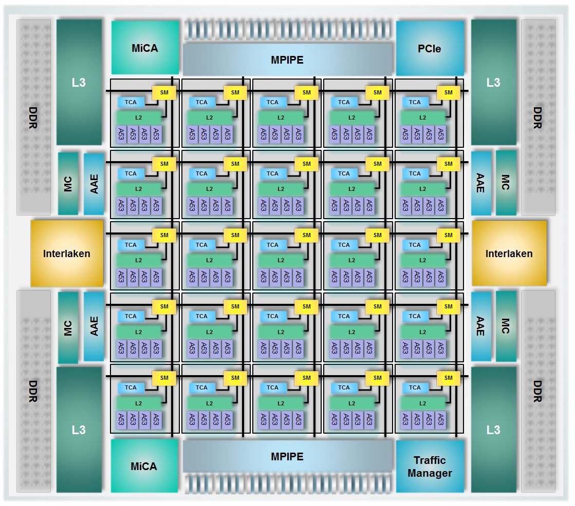 The Tile-Mx100. Source: EZchip
- The industry's first detailed chip featuring 100, 64-bit ARM cores
- The Tile-Mx devices will perform control plane processing and data plane processing
- The 100-core chip will have 100 Gigabit Ethernet ports and support 200 Gigabit duplex traffic
EZchip has detailed the industry's first 100-core processor. Dubbed the Tile-Mx100, the processor will be the most powerful of a family of devices aimed at such applications as software-defined networking (SDN), network function virtualisation (NFV), load-balancing and security. Other uses include video processing and application recognition, to identify applications riding over a carrier's network.
Known for its network processors, EZchip has branched out to also include general-purpose processors following its acquisition of multicore specialist, Tilera. It now competes with such companies as Broadcom, Cavium and Intel.
What's new about the EZchip Tile-Mx100 is that it is the first such processor with 100 cache-coherent programmable CPU cores and it is by far the largest 64-bit ARM processor yet announced
EZchip's NPS network processor is a custom IC designed to maximise packet-processing performance. The Tile-Mx also targets networking but using standard ARM cores. Engineers will benefit from open source software, third-party applications and ARM development tools. "We believe the market needs a standard, open architecture," says Amir Eyal, vice president of business development at EZchip.
"A multicore standard processor tailored for networking is nothing new; numerous such processors have been available for years from several vendors," says Tom Halfhill, senior analyst at The Linley Group. "What's new about the EZchip Tile-Mx100 is that it is the first such processor with 100 cache-coherent programmable CPU cores and it is by far the largest 64-bit ARM processor yet announced."
EZchip has detail three Tile-Mx devices, the most powerful being the Tile-Mx100 that uses 100, 64-bit ARM Cortex-A53 cores. The Cortex-A53 is newer and smaller than the Cortex-A57, and has a relatively low power consumption. Handset and tablet designs are also using the ARM Cortex-A53 core. Both the A53 and A57 cores use the ARMv8-A instruction set.
"We have taken the A53 in order to put more cores on the die," says Eyal. "The idea with networking applications is that the more packets you can process in parallel, the better." A chip hosting many, smaller cores helps meet this goal.
Tile-Mx architecture
The Tile-Mx100 device will process traffic at rates up to 200 Gigabit-per-second (Gbps) rates, or 200 Gbps duplex. In contrast, EZchip's NPS family of devices has a roadmap with a traffic processing performance of 400 Gbps to 800 Gbps duplex.
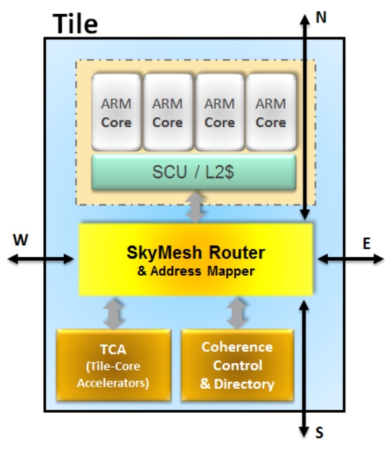
The Tile-Mx uses a two-level architecture. The 100 cores are partitioned into 25 processing clusters or tiles, each comprising four ARM cores that share network acceleration hardware and level-2 cache memory. Each tile also features router hardware, part of the chip's interconnect network that handles the tile's input/ output (I/O) requirements.
 Source: EZchip
"The key technology for the Tile-Mx architecture is the interconnect that enables 100 CPUs to be connected in a coherent manner," says Jag Bolaria, principal analyst at The Linley Group.
"There are five different networks [part of the mesh] that interconnect the 100 cores in parallel, preventing bottlenecks and contention," says Eyal. The mesh also ensures that each core can talk to the chip's I/O and to the memory. The mesh is a fifth iteration, having been improved with each generation of chip design, says Eyal, and has a total bandwidth of 25 Terabits.
The mesh also implements cache coherency, an important aspect of multi-processor design that ensures that cache memory is updated when accessed by any of the cores without needing to introduce idle states first.
Other chip features include a traffic manager, essentially the one used for EZchip's NPUs, which prioritises traffic, allocates bandwidth and prevents packet loss. There are also hardware units (see MiCA blocks in main chip diagram), developed by Tilera, which do preliminary packet classification before presenting the packets to the cores.
The chip's I/O includes 1, 10, 25, 40, 50 and 100 Gigabit Ethernet interfaces, the Interlaken interface and PCI Express, used to connect the chip to a host processor such as an Intel x86 microprocessor.
The idea with networking applications is that the more packets you can process in parallel, the better
EZchip is not detailing the device's interface mix or such metrics as the chip's pin-count, clock speed or power consumption. However, EZchip says the chip's power consumption will be under 100W.
When a packet is presented to the chip, it is assigned to a core which processes it to completion before sending it typically to the I/O. For the programmer, the 100-core device appears as a single processor; it is the hardware on-chip that handles the details, sending an incoming packet to the next free core.
Ezchip shows examples of possible platforms that could use the Tile-Mx.
One is a 1-rack-unit-high pizza box in the data centre used to deliver virtual network functions. Such a NFV server would benefit from the Tile-Mx's hardware-accelerated table look-ups, packet classification and packet flow management in and out of the device. Another design example is using the device for an intelligent network interface card (NIC) in a standard Intel x86-based server.
The two other Tile-Mx family devices will use 36 and 64 Cortex-A53 cores. First Tile-Mx samples are expected in the second half of 2016.
Multicore trends
The Linley Group says that despite the unprecedented 100 ARM cores, EZchip's family of device faces competition. Moreover, the trend to increase core-count has its limits.
EZchip is already shipping a 72-core processor it acquired from Tilera although the device is not ARM-based. And Cavium's largest processor has 48 cores, says Halfhill. Broadcom's largest processor has only 20 cores, but those CPUs are quad-threaded, so the processor can handle up to 80 packet streams. "Not quite as many as the Tile-Mx100, but it is in the same ballpark," says Halfhill.
"Keep in mind that Tile-Mx100 production is about two years out; a lot can happen in two years," adds Halfhill.
According to Bolaria, multicore designs are good for applications that are highly parallelised such as packet processing and deep packet processing. But NPUs are better if all that is being done is packet processing.
"Many cores is not particularly good for applications that need good single-thread performance," says Bolaria. "This is where [an Intel] Xeon will shine — for applications such as high-performance computing, simulations and algorithms."
Coherent interconnects also limit CPU scaling, says Bolaria. Tile-Mx gets around the interconnect limitation by clustering four ARM cores into a tile, so that effectively 25 nodes only are connected. "With more nodes, it becomes difficult to maintain cache coherency and performance," says Bolaria.
Another limitation is partitioning applications into smaller chunks for execution on 100 cores. Some tasks are serial by nature and cannot benefit from parallel processing. "Amdahl’s law limits performance gains from adding more CPUs," says Bolaria.
Photonics and optics: interchangeable yet different
Many terms in telecom are used interchangeably. Terms gain credibility with use but over time things evolve. For example, people understand what is meant by the term carrier [of traffic] or operator [of a network] and even the term incumbent [operator] even though markets are now competitive and 'telephony' is no longer state-run.
"For me, optics is the equivalent of electrical, and photonics is the equivalent of electronics - LSI, VLSI chips and the like" - Mehdi Asghari
Operators - ex-incumbents or otherwise - also do more that oversee the network and now provide complex services. But of course they differ from service providers such as the over-the-top players [third-party providers delivering services over an operator's infrastructure, rather than any theatrical behaviour] or internet content providers.
Google is an internet content provider but with its gigabit broadband service it is rolling out in the US, it is also an operator/ carrier/ communications service provider. And Google may soon become a mobile virtual network operator.
So having multiple terms can be helpful, adding variety especially when writing, but the trouble is it is also confusing.
Recent discussions including interviewing silicon photonics pioneer, Richard Soref, raised the question whether the terms photonics and optics are the same. I decided to ask several industry experts, starting with The Optical Society (OSA).
Tom Hausken, the OSA's senior engineering & applications advisor, says that after many years of thought he concludes the following:
-
People have different definitions for them [optics and photonics] that range all over the map.
-
I find it confusing and unhelpful to distinguish them.
-
The National Academies's report is on record saying there is no difference as far as that study is concerned.
-
That works for me.
Michael Duncan, the OSA's senior science advisor, puts the difference down to one of cultural usage. "Photonics leans more towards the fibre optics, integrated optics, waveguide optics, and the systems they are used in - mostly for communication - while optics is everything else, especially the propagation and modification of coherent and incoherent light," says Duncan. "But I could easily go with Tom's third bullet point."
"Photonics does include the quantum nature, and sort of by convention, the term optics is seen to mean classical" - Richard Soref
Duncan also cites Wikipedia, with its discussion of classical optics that embraces the wave nature of light, and modern optics that also includes light's particle nature. And this distinction is at the core of the difference, without leading to an industry consensus.
"Photonics does include the quantum nature, and sort of by convention, the term optics is seen to mean classical," says Richard Soref. He points out that the website Arxiv.org categorises optics as the subset of physics, while the OSA Newsletter is called Optics & Photonics News, covering all bases.
"Photonics is the larger category, and I might have been a bit off base when throwing around the optics term," says Soref. If only everyone was as off base as Professor Soref.
"We need to remember that there is no canonical definition of these terms, and there is no recognised authority that would write or maintain such a definition," says Geoff Bennett, director, solutions and technology at Infinera. For Bennett, this is a common issue, not confined to the terms optics and photonics: "We see this all the time in the telecoms industry, and in every other industry that combines rapid innovation with aggressive marketing."
That said, he also says that optics refers to classical optics, in which light is treated as a wave, whereas photonics is where light meets active semiconductors and so the quantum nature of light tends to dominate. Examples of the latter would be photonic integrated circuits (PICs). "These contain active lasers components, semiconductor optical amplifiers and photo-detectors " says Bennett. "All of these rely on quantum effects to do their job."
"We need to remember that there is no canonical definition of these terms, and there is no recognised authority that would write or maintain such a definition" - Geoff Bennett
Bennett says that the person who invented the term semiconductor optical amplifier (SOA) was not aware of the definition because the optical amplifier works on quantum principles, the same way a laser does. "So really it should be a semiconductor photonic amplifier," he says.
"At Infinera, we seem for the most part to have abided to the definitions in terminology that we use, but I can’t say that this was a conscious decision," says Bennett. "I am sure that if our marketing department thought that photonic sounded better than optical in a given situation they would have used it."
Mehdi Asghari, vice president, silicon photonics research & development at Mellanox, says optics refers to the classical use and application of light, with light as a ray. He describes optics as having a system-level approach to it.
"We create a system of lenses to make a microscope or telescope to make an optical instrument using classical optics models or we use optical components to create an optical communication system," he says. This classical or system-level perspective makes it optics or optical, a term he prefers. "We are not concerned with the nature - particle versus wave - of light, rather its classical behaviour, be it in an instrument or a system," he says.
But once things are viewed closer, at the device level, especially devices comparable in size of photons, then a system-level approach no longer works and is replaced with a quantum approach. "Here we look at photons and the quantum behaviour they exhibit," says Asghari.
In a waveguide, be it silicon photonics (integrated devices based on silicon), a planar lightwave circuit (glass-based integrated devices), or a PIC based on III-V or active devices, the size of the structure or device used is often comparable or even smaller than the size of the photons it is manipulating, he says: "This is where we very much feel the quantum nature of light, and this is where light becomes photons - photonics - and not optics."
ADVA Optical Networking's senior principal engineer, Klaus Grobe, held a discussion with the company's physicists, and both, independently, had the same opinion.
"Both [photonics and optics] are not strictly defined," he says. "Optics clearly also includes classic school-book ray optics and the like. Photonics already deals with photons, the wave-particle dualism, and hence, at least indirectly, with quantum mechanics, and possibly also quantum electro-dynamics (QED)."
Since in fibre-optics for transport, ray-propagation models no longer can be used, and also since they rely on the quantum-mechanical behaviour, for example of diode receivers, fibre-optics are better filed under photonics, says Grobe: "But they are not called fibre-photonics".
So, the industry view seems to be that the two terms are interchangeable but optics implies the classical nature of light while photonics suggests light as particles. Which term includes both seems to be down to opinion. Some believe optics covers both, others believe photonics is the more encompassing term.
Mellanox's Asghari once famously compared photons and electrons to cats and dogs. Electrons are like dogs: they behave, stick by you and are loyal; they do exactly as you tell them, he said, whereas cats are their own animals and do what they like. Just like photons. So what is his take?
He believes optics is more general than photonics. He uses the analogy of electrical versus electronics to make his point. An electronics system or chip is still an electrical device but it often refers to the integrated chip, while an electrical system is often seen as global and larger, made up of classical devices.
"For me, optics is the equivalent of electrical, and photonics is the equivalent of electronics - LSI, VLSI chips and the like," says Asghari. "One is a subset or specialised version of the other due to the need to get specific on the quantum nature of light and the challenges associated with integration."
"Optics refers to all types of cats, be it the tiger or the lion or the domestic pet. Photonics refers to the so called domestic cat that has domesticated and slaved us to look after it" - Mehdi Asghari
To back up his point, Ashgari says take a look at older books and publications that use the term optics. The term photonics started to be used once integration and size reduction became important, just as how electrical devices got replaced with electronic devices.
Indeed, this rings true in the semiconductor industry: microelectronics has now become nano-electronics as CMOS feature sizes have moved from microns to nanometer dimensions.
And this is why optical fibre or the semiconductor optical amplifier are used because these terms were invented and used when the industry was primarily engaged with the use of light at a system level and away from the quantum limits and challenges of integration.
"In short, photonics is used when we acknowledge that light is made of photons with all the fun and challenges that photons bring to us and optics is when we deal with light at a system level or a classical approach is sufficient," says Asghari.
Happily, cats and dogs feature here too.
"Optics refers to all types of cats, be it the tiger or the lion or the domestic pet," says Asghari. "Photonics refers to the so called domestic cat that has domesticated and slaved us to look after it."
Last word to Infinera's Bennett: "I suppose the moral is: be aware of the different meanings, but don’t let it bug you when people misuse them."
Q&A with Richard Soref - Final Part
In the final part of the interview with Gazettabyte, Richard Soref talks about hybrid and monolithic integration, mid-infrared optics, how his photonics predictions made in a 2006 paper have fared, 2-micron-based optical communications, and his talk at OFC in March.
 "In a rosy future, every smart phone, tablet, wrist watch, and hand-held device would contain one of these chemical-medical-physical sensors."
Richard Soref
Q: The distinction between monolithic and hybrid integration? Arguably all silicon photonics is hybrid integration.
RS: Silicon photonics is mostly monolithic and that is its advantage. Hybrid integration occurs when structures from two different material systems are combined, usually by bonding. When describing the construction of silicon photonics, if we include the germanium laser on silicon, then it is possible to make every component in a chip network from Group IV materials, and this qualifies as monolithic integration.
How important is optical performance using either hybrid or a monolithic design? Is this an academic question or are there differences and hence issues to consider when making a device monolithically or hybridly?
RS: There are real-world issues to consider when evaluating the relative performance of hybrid and monolithic. I don’t know whether hybrid integration is CMOS-foundry-compatible but I suspect that it is. I feel that hybrid integration of III-V laser diodes on silicon or germanium is quite practical, both for telecom and mid infrared. The heterogeneous approach is an excellent, viable solution until germanium-tin (GeSn) laser diodes come along.
Considerable investment is required to make monolithic real. Once actual, it should be more cost-effective than hybrid. The definition of monolithic has vague areas. Is epitaxial growth of III-V on silicon monolithic? Perhaps. If you bond a Group IV nano-membrane onto silicon or germanium, is that monolithic? Probably. We need clearer terminology.
The comparison you’re asking for probably comes down to a performance comparison of III-V and Group IV laser diodes and photo-detectors.
Regarding the economics of silicon photonics, one important issue is the cost of silicon photonics compared to copper. This looks like a major factor limiting silicon photonics adoption. Do you have a view on cost?
RS: These economics are outside my areas of expertise, but I’ll take a stab at it.
Active optical cables are one of several possible killer applications of silicon photonics I don’t know the actual numbers but am guessing that the photonic cost is already below the copper coax cost and is capable of further reduction. Data centres are validating silicon photonics adoption.
A general proposition is that ubiquitous photonics could improve our lives. Mass production at very low cost is on the horizon for silicon photonic integrated circuits (PICs). Once the high-volume, high-impact applications are known, the factory can target them. The global silicon infrastructure could push silicon PICs into the lead. Job creation, industrial competitiveness and other benefits to society will flow from high-yield PICs and opto-electronic integrated circuits (OEICs) made on large wafers. Niche applications and boutique chips may offer important functionality but at higher costs, and for those the silicon may not compete well with III-Vs.
In your paper, The Past, Present and Future of Silicon Photonics, published in 2006, you say that no one can foresee the future and that all one can do is make educated guesses. You then go on and make the following predictions shown in the table below.
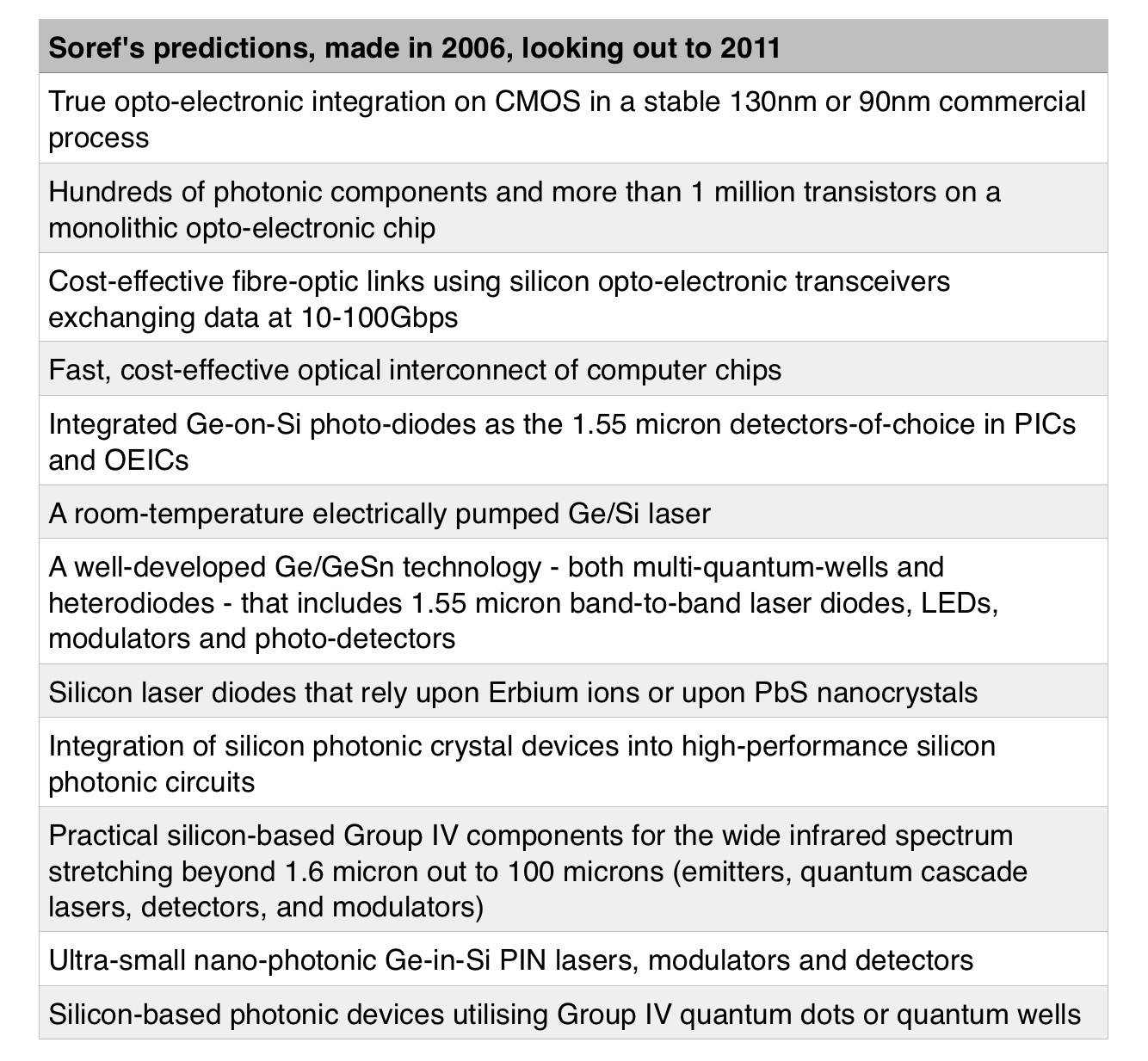
What comments do you have, given the benefit of hindsight?
RS: Well, the scorecard is mixed on these prognostications. A few came true, some are on the verge, others are stuck such as the Erbium-silicon and lead-sulphide-silicon lasers. The mega-transistor OEIC has not yet arrived. The germanium-on-silicon heterolaser diode came true. The high threshold of this laser can be reduced by adding tensile strain and germanium quantum wells, but even after that has been done I feel that this laser’s efficiency will not match that of its III-V competitors.
Efficiency prospects are better for germanium-tin (GeSn). The optically-pumped GeSn laser was just demonstrated in Germany and now we are close to the monolithic on-chip germanium-tin laser diode, although it will emit at 2 microns instead of 1.55 microns.
When I read the press releases of Intel, Cisco, IBM, Mellanox, Luxtera, STMicroelectronics, PhotonIC, IME and imec, I get the impression that major progress has been made in commercial 100 Gigabit-per-second transceiver chips and active optical cables, all of these using hybrid light sources and the germanium photodiodes that I predicted.
Looking at the wide infrared spectrum, the predicted results from 5 to 100 microns have not materialised. However, results are excellent in the 1.6 to 5 micron range. The wavelength-scale components are still on the wanted list, although such modulators and detectors have appeared with a plasmonic flavour.
The GeSn quantum wells arrived in Ghent, Belgium in 2012 and were explored further in Stuttgart, Germany. I believe that a fully fledged silicon-germanium-tin (SiGeSn) technology is unfolding before our eyes today.
The competence of Group IV photonics in so many different scientific areas is its strength and survival mechanism.
In your Photonics West talk in 2013, you talk about silicon opto-electronic mid-infrared system-on-chip. You highlight several interesting application areas including chemical-bio-physical sensing, medical diagnostics, environmental monitoring and high-speed comms at 2 micron. Is sensing a distinct category, and if so, how does it differ from medical diagnostics and environmental monitoring?
RS: Medical diagnostics, industrial process control, and environmental monitoring are all within the same sensing category as chem-bio-physical sensing. That’s why on-chip sensing via photonic techniques is a very broad category. Over time, commercial sales of these photonic sensors - including disposables - could eclipse those of optical interconnects.
How should these mid-infrared applications be seen alongside SiP for telecom and datacoms? Are the two distinct or will developments in mid-infrared applications provide volumes needed that will benefit datacom and telecom silicon photonics at 1.55 microns and below?
RS: Ultra-fast data transmission in the 2 micron band for long-haul and short-haul links arises from the new generation of hollow-core photonic bandgap fibres currently with a loss of 2dB per kilometer. The idea here is that the new 2 micron room-temperature fibre communications will be a practical supplement to current 1.55 micron equipment, and that the various 2 micron connections are not intended to replace existing 1.55 micron infrastructure. In other words, 2 microns expands the global network capacity and does so with low energy consumption. The chip volumes needed at 2 microns will benefit 1.55 microns and vice versa.
What are the main challenges as you see it for these applications? And are these applications a decade behind datacom and telecom because there are no Intels, Ciscos or silicon photonics start-ups driving them?
RS: The main challenge I see for 2 microns is developing the high performance foundry-based room-temperature opto-electronic transceiver chips. I visualise cost-effective germanium-tin (GeSn) photo-detectors and soon GeSn laser diodes integrated in silicon-on-insulator (SOI) waveguide technology with SOI free-carrier modulators. This is a natural sweet-spot for monolithic Group IV photonics.
And no, these applications are not a decade behind because an excellent start has already been made on sensors and 2 microns by researchers in the US, Europe and Asia, even without those start-ups.
The challenge I see in sensors is for practitioners to thread their way through the thicket of reported results on chip-scale refractometers, spectrometers, microfluid channels, label-free detection, resonators, trace-gas concentrators, and plasmonic reflectors, so as to converge upon sensitive, practical solutions.
Parts-per-billion photonic sensors can compete with electronic sensors. Financial investment will actualise the sensor vision and the 2-micron dream. A mixture of technical demonstrators, faith, and venture capital should suffice. Which comes first? Is this a chicken-and-egg question?
At the upcoming OFC 2015 in March, you are to give a talk. What will be the theme?
RS: My mid-infrared talk has a fibre theme and a sensor theme—both about Group IV foundry chips made at low cost. I just described how the fast, energy-efficient 2 micron fibre-optic transceiver chip could be developed with GeSn and SOI. Also, I feel that photonic sensing has tremendous untapped potential including disposables and tiny sensors enabled by battery-powered on-chip nano-lasers.
In a rosy future, every smart phone, tablet, wrist watch, and hand-held device would contain one of these chemical-medical-physical sensors. There are terrific network possibilities. A group of such portable, co-operating sensors, widely dispersed in geography, could be linked by the global cell-phone network or the internet cloud because these photonics will become mainstays of the internet-of-things.
You said as an aside in your 2013 talk that "germanium is the new silicon". What did you mean by that and should we all be looking at 'Germanium Photonics'?
RS: We should be. Germanium has a short wave and a long wave role to play. Germanium shines at 1.6 microns with the laser, the famous photo-detector, and the modulators employing free-carrier, Franz-Keldysh and quantum-confined Stark effects. Germanium is a fine buffer layer on silicon, functioning as an epitaxy platform for SiGeSn. With its high transparency over 1.8 to 15 microns, germanium is superior to silicon over the 8 to 15 micron range where silicon has 2 to 10 dB/cm of loss.
Successful waveguiding experiments in germanium over 2 to 6 microns have confirmed its infrared value for filters, resonators, interconnects and photonic crystals, while waveguide demonstrations over 6 to 14 micron are expected. Germanium is a stellar nonlinear optical material because its third-order susceptibility is much larger than that of silicon. Hence germanium offers superior four-wave mixing, Raman lasing and Brillouin gain, assuming pump wavelengths longer than 3.4 microns. Germanium serves in heterostructures and quantum structures as a barrier to GeSn. Quantum dots are available. Doped germanium can be a plasmonic conductor. Overall, self-contained photonics.
Lastly, what opportunities excite you most and if you were giving advice to young engineers and researchers looking at silicon photonics/ Group IV photonics, what would you recommend they focus on over the next 10 years?
RS: I think that young scientists and engineers entering this field should aim at ambitious, modern goals. They could investigate significant trends-in-motion or exotic emerging directions.
Regarding trends, the young engineers have opportunities for impact in photonic sensors, terabit-per-second optical interconnect devices, analogue-and-digital mixed signal chips, microwave photonics of several kinds, space-division and mode-division multiplexing, night-vision imaging, beam steering, and control of microwave antennas. Their talents could create new PICs and OEICs for practical outcomes.
For the more speculative category, the young scientists could focus on pathfinding forms of optical computing, as opposed to types discredited in the past. They could make advances in quantum integrated photonics, to use Professor Ben Eggleton’s term, getting results in quantum computing, secure communications and metrology.
In a similar vein, some good targets are the Ising machine and the neural-network computer with its training sets. Linear-and-nonlinear optics at Terahertz and long wave infrared could be explored.
I’m excited by the topic of nano-laser diodes; an all-Group IV photonics version rather than the metal-coated kind. I visualise a two-dimensional germanium photonic crystal grown directly on an oxidised SOI waveguide that possess a surface grating. A wavelength-scale GeSn gain region is embedded in the line-defect cavity zone where lateral PIN injection takes place. Then, this surface emitting nano laser is vertically coupled to the SOI beneath it.
For the first part of the interview, click here
Between 1998 and 2003, Professor Soref wrote 36 short poems that were published in internet magazines, some are which are still online. He is also a distinguished photographer, click here to see some of his work. "I gravitate to art forms of which science is one," he says.
Q&A with photonics pioneer, Richard Soref - Part 1
Richard Soref has spent over 50 years researching photonics, contributing groundbreaking work in the areas of liquid crystals, silicon photonics and the broader topic of mid-infrared wavelengths and Group IV photonics. For 27 years he was employed at the Air Force Research Laboratory. He has also worked at the Sperry Research Center, the MIT Lincoln Laboratory, and is now a research professor at the University of Massachusetts in Boston.
In part 1 of a two-part interview with Gazettabyte, he details his research interests, explains what is meant by Group IV photonics, and discusses why photonics has not matched the semiconductor industry in terms of integration, and how that could change.
Optics is a seemingly small subset of physics but really optics is a huge field with a deep, variegated nature waiting to be discovered
Richard Soref
Q: Having gained your Ph.D. in 1963, you have spent your career in what you call the science of light. What is it about photonics that you find so captivating?
RS: I’ve been drawn to its diversity and classical beauty. Photonics used to be called optics until it was re-labelled by the OSA. Optics is a seemingly small subset of physics but really optics is a huge field with a deep, variegated nature waiting to be discovered. To make progress, you need multiple disciplines, and I’ve always been captivated by the materials science aspect that opens the door to new physics and new devices.
Can you outline your career and how you ended up as a research professor at the University of Massachusetts at Boston?
RS: A general outline is that I chose employers who would encourage exploration of new avenues, would give me freedom to fly or fall – and both are built into research. Basic research is where my talents and passion align. And it helps to be obsessive.
In the early years, I worked mostly alone. Then the pleasures of collaboration became important, and for decades I have been fortunate to have outstanding research partners who did heavy lifting of things like quantum mechanics and electromagnetic modelling.
At Lincoln Lab, I continued the nonlinear optical studies that I began during my Stanford Ph.D. work. Sperry Research was an excellent environment until it fell victim to the corporate research shutdown contagion. Ironically or prophetically, impurity-doped silicon infrared sensors were an early focus at Sperry.
Lithium niobate sparked my 40-year interest in electro-optics: Pockels [effect], Kerr [electro-optic effect], Franz-Keldysh [effect] and more. My extensive work on liquid crystals gained a lot of traction, and at an Information Display show I met scientists from South Korea who told me that my early papers helped them with their commercial flat-panel TV products. It was fulfilling to hear that.
Apart from some governmental distractions, the Air Force Research Laboratory (AFRL) years were a happy time and I welcomed the support of the Air Force Office of Scientific Research (AFOSR); the AFOSR is a national treasure.
Fibre-optic telecom emerged in 1985 when I was at AFRL. The fibres needed semiconductor assistance, I felt. That’s when the new silicon insights came to me. I’m glad that I was able in 1989 to identify silicon-on-insulator (SOI) as the primary waveguided-network platform, and I’m gratified that brilliant and innovative research groups around the world entered this field early on. They strived successfully to perfect this technology. To do my part, I tried to surround the problem in a 1985-2015 series of papers, among them my 1991 silicon-germanium-tin (SiGeSn) direct-gap prediction and my 1992 opto-electronic integrated circuit (OEIC) proposal. My most-cited work is a 1987 paper on free-carrier electro-optics.
Summarising, I had two visions at AFRL: Group IV photonics and long-wave integrated optoelectronics, where long wave denotes anything from two to 200 microns, although the mid-infrared wavelengths are key because of their room temperature possibilities. Perhaps there is a third vision: the multi-technology 3D chip on which seven technologies including bio-chemical could be combined.
Sadly those creative years drew to a close when the Massachusetts laboratory was shut down by the Air Force and the party moved to Wright Patterson AFB in Ohio. At that point, I joined the University of Massachusetts in Boston to stay near family and to keep the technical flame alive in research. I’m still collaborating with wonderful people, most of them young.
Can you provide rigour regarding some definitions? Starting with silicon photonics, silicon mid-infrared optics and Group IV photonics, can you define each and do you have a preference for a particular term?
RS: The silicon-photonics term is strongly entrenched in the global community. The phrase includes on-chip germanium photo-detectors and presumably germanium lasers. Nevertheless, I think this term is a bit narrow or misleading about the silicon-germanium-tin materials (SiGeSn) that likely will be used in the monolithic silicon chip of the future.
I am in the minority when I say that I prefer the wider term Group IV photonics (GFP) which takes into account those three-part alloys as well as diamond and graphene. This GFP term was coined in 2003 in my office at Hanscom when Greg Sun and I were dreaming constructively about a new, dedicated IEEE conference, the international meeting I co-founded in 2004.
In the coming years, the purely photonic integrated circuit, the PIC chip, will evolve, after money is spent, into the opto-electronic chip, and the transistors will be CMOS or BiCMOS or heterojunction bipolar
What about the OEIC, how does it differ from silicon photonics? And lastly, nano-photonics, how does it compare to silicon photonics?
RS: The opto-electronic integrated circuit describes the synergistic marriage of nano-photonics and nano-electronics on the same silicon chip. Others have called this an electronic-photonic integrated circuit or EPIC. In essence, the OEIC is a transistorised photonic chip containing electronic intelligence, signal processing, computation, electrical control of active photonic devices, and perhaps RF wireless transceiving capability, which I strongly advocate.
In the coming years, the purely photonic integrated circuit, the PIC chip, will evolve, after money is spent, into the opto-electronic chip, and the transistors will be CMOS or BiCMOS or heterojunction bipolar. These possibilities illustrate the diversity of GFP.
As for nano-photonics, it is a subset of silicon photonics populated by wave-guided components whose smallest cross-section dimension is 15 to 30 percent of the free-space wavelength. Photonics, like electronics, started as micro and shrank to nano. The term nano means nanometer-scale and applies also to quantum-dot diameter, quantum-well layer thickness and photonic-crystal air hole diameter.
In over half a century, electronics has undergone an extraordinary transformation from simple integrated circuits to profoundly complex ones. Yet while integrated optics was spoken of as early as 1969 in the Bell Labs paper by Stuart Miller, integration has been far more modest. Why?
RS: The main roadblock has been the lack of compelling applications for medium scale and large scale photonic integration. Perhaps this was a lack of vision or a lack of market to drive the integration research.
Another inhibiting factor is the large expense, the cost-per-run of making a photonic integrated circuit, although the OPSIS user foundry [before it closed] and other user facilities have mitigated entry costs to some extent. Additional factors are the area-footprint and volume of the photonic building blocks. The photonic device size is generally larger, or much larger, than the size of the modern individual transistor.
Is this about to change?
RS: To some degree, yes. People are packing photonic components together in a circuit but there are limits on how closely this can be done. These constraints lead me to wonder whether photonic integration will follow the same historical path as micro- and nano-electronics, the same developmental story. Will there be a Moore’s law for photonics with PIC packing density doubling every 18 months? The billion-photonic circuit is not on the cards, so I doubt that the law will hold.
The diffraction limit of optics and the single-mode criteria set lower limits on photonic size, although plasmonic devices go below those dimensional limits and are compatible with photonics.
I see glimmers today of where LSI can make a difference. A near-term use is a 128x128 array of electro-optical phase shifters for optical beam steering. More speculatively, we have electro-optical logic arrays, spectrometers on-chip, optical neural networks, dense wavelength-division multiplexers and demultiplexers, quantum processors, and optical computers using dense nano-LED arrays.
The government has deeper pockets than industry for sustained R&D efforts
What are the major challenges today making optical devices using a CMOS fabrication process?
RS: A partially-met challenge is to actualise a stable and reliable process in a 130nm or 65nm CMOS node for manufacturing the active and passive photonic parts of the on-chip network. We need process procedures for principal components which are recipes defined with a new design library. Whether to standardise photonics is an open question. When and where to place transistor circuits on-chip is a challenge. Putting transistors on a separate chip is a near-term alternative.
It takes art as well as science to determine the opto-electronic layering and to decide whether the available processing temperatures necessitate fabrication at the front end or back end of the overall process.
I believe that a manufacturing initiative is an essential next step for GFP to convince friends and skeptics alike of the long-term commercial and military value of GFP offered in new generations of energy-efficient ultra-performance chipsets. The government has deeper pockets than industry for sustained R&D efforts, so I believe that the Department of Defense can be the force driving GFP expansion into higher realms at very low costs per chip.
That’s why I welcome the new 5-year Integrated Photonics Institute project as part of the National Network for Manufacturing Innovation, funded by the RAMI bill [Revitalize American Manufacturing and Innovation Act]. It is a bill that would train the workforce, while public-private partnerships will transform research into products and will deploy infrastructure that supports US-enterprise competitiveness.
For the second part, click here