
Relentless traffic growth leads to a ROADM rethink
Technology briefing: ROADMs
Lumentum has developed an optical switch to enable reconfigurable optical add-drop multiplexers (ROADMs) to cope with the traffic growth expected over the next decade.
The company’s MxN wavelength-selective switch (WSS) will replace the existing multicast switch used in colourless, directionless and contentionless ROADMs. The Lumentum TrueFlex 8x24 twin switch will enable networking nodes of 400-terabit capacity.
“This second-generation switch is what will take us into the 100 gigabaud and super-channel era of network scalability,” says Brandon Collings, CTO of Lumentum.
ROADMs
ROADMs sit at the mesh nodes in an optical network. Their function is to pass lightpaths destined for other nodes in the network - referred to as optical bypass - and enable the adding and dropping of wavelengths at the node. Such add/drops may be rerouted traffic or provisioned new services.
As network traffic continues to grow, so do the degrees of a ROADM and the ports of its sub-systems. The degree of a ROADM is defined to the number of connections or fibre pairs it can support. In the diagram, a ROADM of degree three is shown.
 A multicast switch-based 3-degree CDC ROADM. Source Lumentum.
It is rare to encounter more than five or six fibre routes leaving any given mesh node in a network, says Lumentum. “But in those fibre routes there is typically a large number of fibres - 64 or 128,” says Collings. “Operators deploy a conduit of fibre between cities.”
When the C-band fills up, an operator will light another fibre pair, taking up another of the ROADM’s degrees. ROADMs built today have 16 degrees. And since a fibre’s C-band can occupy some 30 terabits of data, this is how 400-terabit mesh nodes will be achieved.
“That is a pretty big node but that is the end [of life] capacity,” says Collings. “I don’t think you will find a 400-terabit node today but we build our networks so that they get there, five to eight years from when they are deployed.”
This raises another issue: the length of time it takes for any generational change of a ROADM design to take hold in the network.
“When a new approach comes along, it takes a couple of years for everyone to figure out how they will use it,” says Collings. Then, once a decision is made, it takes another two years to deploy followed by five to eight years before the ROADM node is filled.
“Nothing happens quickly in this business,” says Collings. “But the upside, from a business point of view, is that as things are designed in, they have a long deployment cycle.”
Lumentum illustrates the point with its own products.
The company is seeing growing demand for its dual TrueFlex WSS deployed in route-and-select ROADM architectures. “But we are still seeing growth on the older broadcast-and-select architectures underpinned by singe 1x9 WSSes,” says James Goodchild, director, product line management for wavelength management products at Lumentum.
CDC ROADMs
A colourless, directionless and contentionless (CDC) ROADM uses a twin multicast switch for the wavelength add and drop functions. The input fibre to each degree’s WSS is connected to the output path WSS of each of the ROADM’s other degrees. The input WSS also connects to the drop multicast switch (see diagram above).
Using a WSS on the input path means that only wavelengths of interest are routed to the WSS’ output ports. Hence the ROADM’s reference as a route-and-select architecture.
Using a 1xN splitter array instead of a WSS for the input path results in a broadcast-and-select ROADM. Here, the input fibre’s wavelengths are broadcast to all the N output ports. The high optical loss associated with the splitters is the main reason why CDC ROADM designs have transitioned to the WSS-based route-and-select architecture.
This second-generation switch is what will take us into the 100 gigabaud and super-channel era of network scalability
However, there is still an optical loss issue to be contended with, introduced by the add or drop multicast switch. Accordingly, along with the twin multicast switch are two arrays of erbium-doped fibre amplifiers (EDFAs). One EDFA array is on the drop ports to the MxN multicast switch and the second amplifier array boosts the outputs of the add-path multicast switch before their transmission into the network.
The MxN multicast switch comprises 1xN splitter arrays, N being the number of add-drop ports, and Mx1 selection switches where M is the number of directions the ROADM supports. A typical multicast switch is 8x16: eight being the ROADM’s number of directions and 16 the drop-port count.
Each of the N splitter arrays sends the signals on a drop port to all the Mx1 selection switches where each one pulls off the channel to be dropped. Having a selection switch at each of the multicast switch’s N drop ports is what enables contentionless operation, the avoidance of a collision when the same wavelength is droppedat a node from different degree directions.
MxN switch
Lumentum’s decision to develop the MxN switch to replace the multicast switch follows its study to understand how optical transmission networks will evolve with continual traffic growth.
One development is the adoption of higher-baud-rate, higher-capacity coherent transmissions that require wider channel widths. A 400-gigabit wavelength requires a 75GHz channel compared to the standard 50GHz fixed grid used for 100- and 200-gigabit transmissions. Future transmission speeds of 800 gigabits will use two such channels or 150GHz of spectrum, while a 1 terabit signal is expected to occupy 300GHz of fibre spectrum. “This is how we anticipate coherent transmission evolving,” says Collings.
Moving to wider channels also benefits the ROADM’s cost. If operators continued to use 50GHz channels, the channel count would grow exponentially with the growth in traffic. In contrast, adopting wider channels means the add-drop port count grows only linearly with traffic. “Using wider channels, the advantage is you don't have to support 600 ports of add-drop in your ROADM networks,” says Collings.
But wider channels means greater amplification demands on the EDFA arrays, an issue that will only worsen over time.
Multicast switch-based designs don’t support the wider channels we know are coming
Losing the amp
Because the power spectral density is constant, the power in a channel increases proportionally with its width. For example, a 75GHz channel has 2dB more power compared to a 50GHz channel spacing, a 150GHz channel 5dB more while a 300GHz channel has an extra 8dB.
The EDFA array is engineered to handle the worst case power requirement that occurs when all 16 optical transceivers into the multicast switch go to the same ROADM degree. Here the EDFA must be able to boost all 16 channels.
For a multicast switch with 16 ports, 22dBm amplification is needed for a 150GHz channel which requires going from an uncooled pump design to a cooled pump one. Equally, 25dBm amplification is needed for 300GHz channels. And as the number of degrees grows, so do the demands on the amplification until no practical amplifier design is possible (see diagram).
 The EDFA requirements to compensate for the optical loss of the multicast switch. The complexity of the EDFA design grows with the multicast switch's port count until it becomes insupportable. Source: Lumentum.
“This is not an issue today because we use very modest-sized channels and we engineer our systems to accommodate them,” says Collings. “But if you look forward, you realise they [multicast switch-based designs] don’t support the wider channels we know are coming.”
Using a WSS-based MxN switch solves this issue because, as with the input port WSS of a route-and-select architecture, the switch has a lower optical loss - under 8dB - compared to the 17dB of the splitter-based multicast switch.
The sub-8dB loss is below the threshold where amplification is needed: the optical signal is sufficiently strong at the drop port to be received, as are the added signals for transmission into the network. The resulting removal of the EDFAs simplifies greatly the complexity, size and cost of the CDC ROADM.
“The MxN is a WSS - it’s a router - so it sends all of the light in the direction it is supposed to go,” says Collings. “You can push through the MxN switch channels of any width and of any power because there is no amplifier that needs to be there and be designed appropriately."
The resulting second-generation CDC ROADM design is shown below.
 Source: Lumentum
Lumentum's Goodchild says the 8x24 twin implementation of the MxN switch will be available in the first quarter of 2019.
“Certain systems vendors already have access to samples,” says Goodchild.
Further reading
2D WSSes, click here
ROADMs and their evolving amplification needs, click here
Habana Labs unveils its AI processor plans
Start-up Habana Labs has developed a chip architecture that promises to speed up the execution of machine-learning tasks.
The Israeli start-up came out of secrecy in September to announce two artificial intelligence (AI) processor chips. One, dubbed Gaudi, is designed to tackle the training of large-scale neural networks. The chip will be available in 2019.
 Eitan MedinaGoya, the start-up’s second device, is an inference processor that implements the optimised, trained neural network.
The Goya chip is already in prospective customers’ labs undergoing evaluation, says Eitan Medina, Habana’s chief business officer.
Habana has just raised $75 million in a second round of funding, led by Intel Capital. Overall, the start-up has raised a total of $120 million in funding.
Deep learning
Deep learning in a key approach used to perform machine learning. To perform deep learning, use is made of an artificial neural network with many hidden layers. A hidden layer is a layer of nodes found between the neural network’s input and output layers.
To benefit from deep learning, the neural network must first be trained with representative data. This is an iterative and computationally-demanding process.
The computing resources used to train the largest AI jobs has been doubled every 3.5 months since 2012
Once trained, a neural network is ready to analyse data. Common examples where trained neural networks are used include image classification and for autonomous vehicles.
 Source: Habana Labs
Two types of silicon are used for deep learning: general-purpose server CPUs such as from Intel and graphics processing units (GPUs) from the likes of Nvidia.
Most of the growth has been in the training of neural networks and this is where Nvidia has done very well. Nvidia has a run rate close to $3 billion just building chips to do the training of neural networks, says Karl Freund, senior analyst, HPC and deep learning at Moor Insights & Strategy. “They own that market.”
Now custom AI processors are emerging from companies such as Habana that are looking to take business from Nvidia and exploit the emerging market for inference chips.
“Use of neural networks outside of the Super Seven [hyperscalers] is still a nascent market but it could be potentially a $20 billion market in the next 10 years,” says Freund. “Unlike in training where you have a very strong incumbent, in inference - which could be a potentially larger market - there is no incumbent.”
This is where many new chip entrants are focussed. After all, it is a lot easier to go after an emerging market than to displace a strong competitor such as Nvidia, says Freund, who adds that Nvidia has its own inference hardware but it is suited to solving really difficult problems such as autonomous vehicles.
“For any new processor architecture to have any justification, it needs to be significantly better than previous ones,” says Medina.
Habana cites the ResNet-50 image classification algorithm to highlight its silicon’s merits. ResNet-50 refers to a 50-layer neural network that makes use of a technique called residual learning that improves the efficacy of image classification.
Habana’s Goya HL-1000 processor can classify 15,000 images-per-second using ResNet-50 while Nvidia’s V100 GPU classifies 2,657and Intel’s dual-socket Platinum 8180 CPU achieves 1225 images-per-second.
“What we have architected is fundamentally better than CPUs and GPUs in terms of processing performance and the processing-power factor,” says Medina.
“Habana appears to be one of the first start-ups to bring an AI accelerator to the market, that is, to actually deliver a product for sale,” says Linley Gwennap, president and principal analyst of The Linley Group.
Both Habana and start-up Graphcore expect to have final products for sale this year, he says, while Wave Computing, another start-up, expects to enter production early next year.
“It is also impressive that Habana is reporting 5-6x better performance than Nvidia, whereas Graphcore’s lead is less than 2x,” says Gwennap. “Graphcore focuses on training, however, whereas the Goya chip is for inference.”
Habana appears to be one of the first start-ups to bring an AI accelerator to the market
Gaudi training processor
Habana’s Gaudi chip is a neural-network training processor. Once trained, the neural network is optimised and loaded into the inference chip such as Habana’s Goya to implement what has been learnt.
“The process of getting to a trained model involves a very different compute, scale-out and power-envelopment environment to that of inference,” says Medina.
To put this in perspective, the computing resources used to train the largest AI jobs has been doubled every 3.5 months since 2012. The finding, from AI research company OpenAI, means that the computing power being employed now has grown by over one million times since 2012.
Habana remains secretive about the details of its chips. It has said that the 16nm CMOS Gaudi chip can scale to thousands of units and that each device will have 2 terabits of input-output (I/O). This contrasts with GPUs used for training that do have scaling issues, it says.
First, GPUs are expensive and power-hungry devices. The data set used for training such as for image classification needs to be split across the GPUs. If the number of images - the batch size - given to each one is too large, the training model may not converge. If the model doesn't converge, the neural network will not learn to do its job.
In turn, reducing the batch size affects the overall throughput. “GPUs and CPUs want you to feed them with a lot of data to increase throughput,” says Medina.
Habana says that unlike GPUs, its training processor’s performance will scale with the number of devices used.
“We will show with the Gaudi that we can scale performance linearly,” says Medina. “Training jobs will finish faster and models could be much deeper and more complex.”
 The Goya IC architecture. Habana says this is a general representation of the chip and what is shown is not the actual number of tensor processor cores (TPCs). Source: Habana Labs
Goya inference processor
The Goya processor comprises multiple tensor processor cores (TPCs), see diagram. Habana is not saying how many but each TPC is capable of processing vectors and matrices efficiently using several data types - eight-, 16- and 32-bit signed and unsigned integers and 32-bit floating point. To achieve this, the architecture used for the TPC is a very-long-instruction-word, (VLIW) single-instruction, multiple-data (SIMD) vector processor. Each TPC also has its own local memory.
Other on-chip hardware blocks include a general-purpose engine (GEMM), shared memory, an interface to external DDR4 SDRAM memory and support for PCI Express (PCIe) 4.0.
What we have architected is fundamentally better than CPUs and GPUs in terms of processing performance and the processing-power factor
Habana claims its inference chip has a key advantage when it comes to latency, the time it takes for the inference chip to deliver its answer.
Latency too is a function of the batch size - the number of jobs - presented to the device. Being able to pool jobs presented to the chip is a benefit but not if it exceeds the latency required.
“If you listen to what Google says about real-time applications, to meet the 99th percentile of real-time user interaction, they need the inference to be accelerated to under 7 milliseconds,” says Medina. “Microsoft also says that latency is incredibly important and that is why they can’t use a batch size of 64.”
Habana and other entrants are going after applications where their AI processors are efficient at real-time tasks with a batch size of one. “Everyone is focussing on what Nvidia can’t do well so they are building inference chips that do very well with low batch sizes,” says Freund.
Having a low-latency device not only will enable all sorts of real-time applications but will also allow a data centre operator to rent out the AI processor to multiple customers, knowing what the latency will be for each job.
“This will generate more revenue and lower the cost of AI,” says Medina.
AI PCIe cards
Habana is offering two PCIe 4.0 card versions of its Goya chip: one being one-slot wide and the second being double width. This is to conform to some customers that already use platforms with double-width GPU cards.
Habana’s PCIe 4.0 card includes the Goya chip and external memory and consumes around 100W, the majority of the power consumed by the inference chip.
The card’s PCIe 4.0 interface has 16 lanes (x16) but nearly all the workloads can manage with a single lane.
“The x16 is in case you go for more complicated topologies where you can split the model between adjacent cards and then we need to pass information between our processors,” says Medina.
Here, a PCIe switch chip would be put on the motherboard to enable the communications between the Goya processors.
Do start-ups have a sustainable architectural roadmap that offers innovation beyond just such single-cycle operations?
Applications
Habana has developed demonstrations of four common applications to run on the Goya cards. These include image classification, machine translation, recommendations, and the classification of text known as sentiment analysis.
The four were chosen as potential customers want to see these working. “If they are going to buy your hardware for inference, they want to make sure it can deal with any topology they come up with in future,” says Medina.
Habana says it is already engaged with customers other than the largest data centre operators. And with time, the start-up expects to develop inference chips with tailored I/O to address dedicated applications such as autonomous vehicles.
There are also other markets emerging beside data centres and self-driving cars.
“Mythic, for example, targets security cameras while other start-ups offer IP cores, and some target the Internet of Things and other low-cost applications,” says Gwennap. “Eventually, most processors will have some sort of AI accelerator built-in, so there are many different opportunities for this technology.”
Start-up challenge
The challenge facing all the AI processor start-ups, says Freund, is doing more thandeveloping an architecture that can do a multiply-accumulate operation in a single processor clock cycle, and not just with numbers but withn-dimensional matrices.
“That is really hard but eventually - give or take a year - everyone will figure it out,” says Freund.
The question for the start-ups is: do they have a sustainable architectural roadmap that offers innovation beyond just such single-cycle operations?
“What architecturally are you able to do beyond that to avoid being crushed by Nvidia, and if not Nvidia then Intel because they haven't finished yet,” says Freund.
This is what all these start-ups are going to struggle with whereas Nvidia has 10,000 engineers figuring it out, he warns.
Article updated on Nov 16 to report the latest Series B funding.
Edgecore exploits telecom’s open-networking opportunity
Edgecore Networks is expanding its open networking portfolio with cell-site gateways and passive optical networking (PON) platforms.
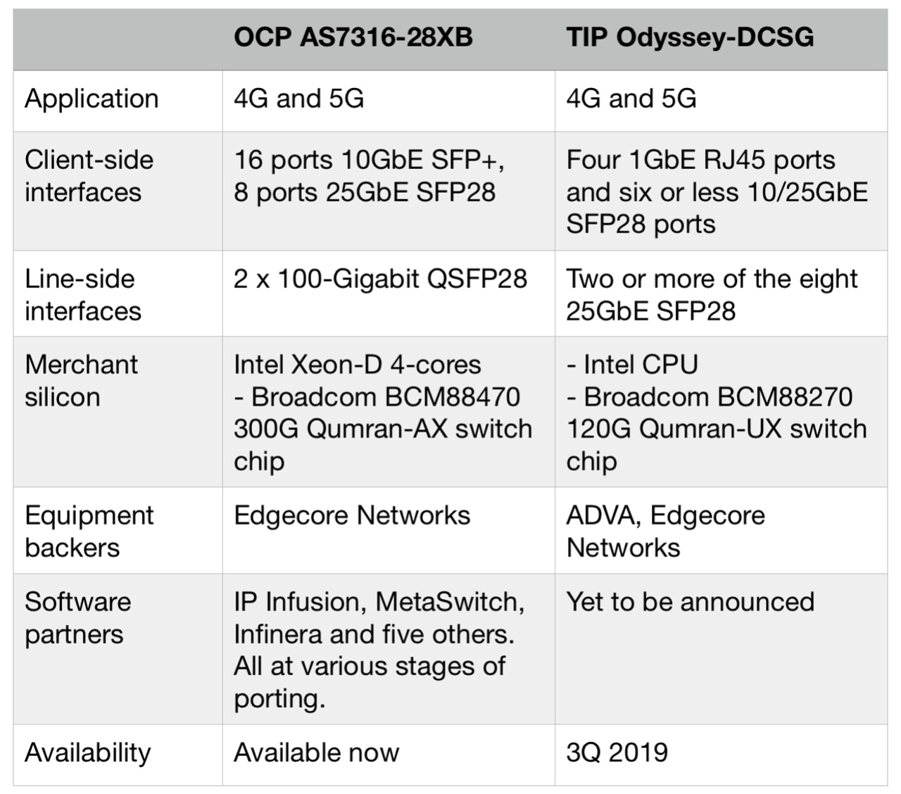
The company is backing two cell-site gateway designs that aggregate traffic from baseband units for 4G and 5G mobile networks. One design is from the Open Compute Project (OCP) that is available now and the second is from the Telecom Infra Project (TIP) that is planned for 2019 (see table).
Edgecore has also announced PON optical line terminal (OLT) platforms addressing 10-gigabit XGS-PON and GPON.
 Source: ADVA, Edgecore Networks
Edgecore is a wholly-ownedsubsidiary of Accton Technology, a Taiwanese original design manufacturer (ODM) employing over 700 networking engineers that reported revenues exceeding $1.2 billion in 2017.
Open networking
Edgecore is a leading proponent of open networking that first data centre operators and now telecom operators are adopting.
Open networking refers to disaggregated designs where the hardware and software comes from separate companies. The hardware is a standardised white box developed in an open framework, while the accompanying software can be commercial code from a company or open-sourced.
Our focus is on all those attributes of open networking: disaggregation, the hardware and software design of standard platforms, and making those designs open
Telecom networks have traditionally been built using proprietary equipment from systems vendors that includes the complete software stack. But the leading telcos have moved away from this approach to avoid being locked into a systems vendor's roadmap. Instead, they are active in open frameworks and are embracing disaggregated open designs, having seen the benefits achieved by the internet content providers that pioneered the approach.
“The IT industry for years have been buying servers and purposing them for whatever application they are designated for, adding an operating system and application software on top,” says Mark Basham, vice president business development and marketing, EMEA at Edgecore. “Now we are seeing the telecom industry shift to that model; they see where the value should be.”
White-box platforms built using merchant silicon promise to reduce the number of specialised platforms in an operator’s network, reducing costs by simplifying platform qualification and support.
“Our focus is on all those attributes of open networking: disaggregation, the hardware and software design of standard platforms, and making those designs open,” says Bill Burger, vice president, business development and marketing for North America at Edgecore.
OCP, TIP and ONF
Edgecore is active in three leading open framework initiatives whose memberships include large-scale data centre operators, telcos, equipment makers, systems integrators, software partners and chip players.
Edgecore is a member of OCP that was founded to address the data centre but now plays an important role in telecoms. The company is also part of TIP that was established in 2016 and includes internet giants Facebook and Microsoft as well as leading telecom operators, systems vendors, components players and others. Edgecore is also a key white-box partner as part of the Open Networking Foundation’s (ONF) reference-design initiative.
 Edgecore Networks' involvement in the ONF's reference design projects. Diagram first published in July 2018. Source: ONF.
Cell-site gateways
Edgecore has announced the availability of its AS7316-26XB, the industry’s first open cell-site gateway white-box design from the OCP that originated as an AT&T specification.
The company is also active in TIP’s cell-site gateway initiative. Edgecore will make and market the Odyssey Disaggregated Cell Site Gateway (Odyssey-DCSG) design that is backed by TIP’s operator members Telefonica, Orange, TIM Brazil and Vodafone. BT is also believed to be backing the TIP gateway.
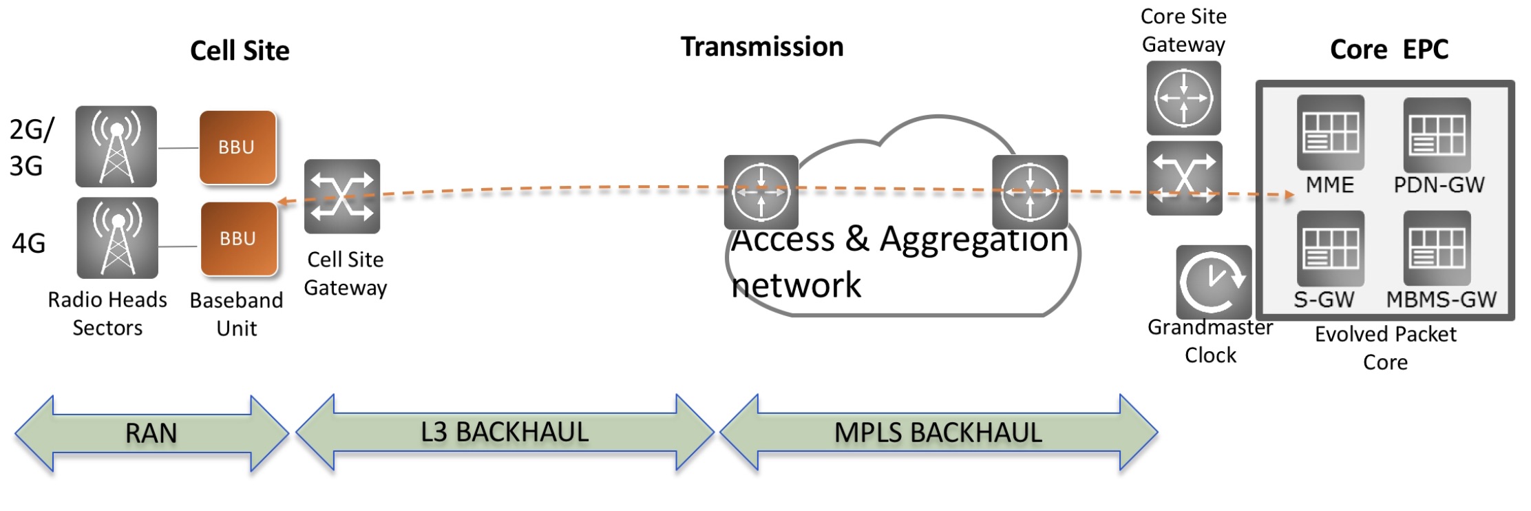
The gateway aggregates the radio baseband unit (BBU) at a cell site back into the transport network.
The OCP cell-site gateway has a more advanced specification compared to the Odyssey. The AS7316-26XB uses a more powerful Intel processor and employs a 300-gigabit Broadcom Qumran-AX switch chip that aggregates the baseband traffic for transmission into the network.
The platform’s client-side interfaces include 16 SFP+ ports that supports either 1 Gigabit Ethernet (GbE) SFP or 10GbE SFP+ pluggable modules, eight 25GbE ports that accommodate either 10GbE SFP+ or 25GbE SFP28 modules, and two 100GbE QSFP28 uplinks. Some of the 25GbE ports could be used to expand the uplink capacity, if needed.
In contrast, the TIP Odyssey-DCSG platform uses a 120-gigabit Qumran switch chip while its interfaces include provide four 1GbE RJ45 ports and eight 10GbE or 25GbE SFP28 ports. Accordingly, the platform’s uplinks are at 25GbE.
“They [the OCP and TIP gateways] are very different boxes in terms of their performance,” says Basham.
Current deployed mobile platforms don't have sufficient capacity to support LTE Advanced Pro, never mind 5G, says Basham: “All the operators are looking at what is the right time to insert these boxes in the network.”
Telcos need to decide how much they are willing to spend up front. They could deploy a larger capacity but costlier cell-site gateway to future-proof their mobile backhaul for up to a decade. Or they could install the smaller-capacity Odyssey-DCSG that will suffice for five years before requiring an upgrade.
Given that the largest operators will deploy the gateways in units of hundreds of thousands, the capital expenditure outlay will be significant.
Basham says there will be a family of cell-site gateways and points out that the TIP specification originally had three ‘service configurations’. The latest TIP specification document now has a fourth service configuration that differs significantly from the other three in its port count and capabilities. “It shows that there is no one-size-fits-all,” says Basham.
The company also has announced two open disaggregated PON products, part of the OCP.
The ASXvOLT16 is a 10-gigabit OLT platform that supports XGS-PON and NG-PON2. The open OLT platform uses Broadcom’s 800-gigabit Qumran-MX switch chip and its BCM68620 Maple OLT device.
The platform’s interfaces includes 16 XFP ports supporting 10-gigabit optics while for the uplink traffic, four 100GbE ports are used. Each 10-gigabit interface will support 32 or 64 PON optical network units (ONU) typically.
“To support NG-PON2 will require the virtual OLT hardware abstraction layer to be adapted slightly, and also firmware to be put on the Broadcom chips,” says Basham. “The big difference between XGS-PON and NG-PON2 is in the plug-in optics.” More costly tunable optics will be required for NG-PON2. The 1 rack unit (1RU) PON OLT design is available now.
Edgecore has also contributed GPON OLT designs that conform with Deutsche Telecom’s Open GPON OLT design. The Edgecore ASGvOLT32 and ASGvOLT64 GPON OLTs support 32- and 64-GPON ports, respectively, while there are two 100GbE and eight 25GbE uplink ports.
The two GPON OLTs will sample in the first quarter of 2019, moving to volume production one quarter later.
We are at the cusp of bringing together all the parts to make Cassini a deployable solution
Cassini
Edgecore is also bringing its Cassini packet-optical transport white-box platform to market.
Like TIP’s Voyager box, Cassini uses the Broadcom StrataXGS Tomahawk 3.2-terabit switch chip. But while the Voyager comes with built-in coherent interfaces based on Acacia’s AC-400 module, Cassini is a modular design that has eight card slots. Each slot can accommodate one of three module options: a coherent CFP2-ACO, a coherent CFP2-DCO or two QSFP28 100-gigabit pluggables. The Cassini platform also has 16 fixed QSFP28 ports.
Accordingly, the 1.5RU Cassini box can be configured using only the coherent interfaces required. The box could be set up as a 3.2-terabit switch using QSFP28 modules only or as a transport box with up to 1.6 terabits of client-side interfaces and 1.6 terabits of line-side coherent interfaces. This contrasts with the 1RU Voyager that offers 2 terabits of switch capacity with its dozen 100-gigabit client-side interfaces and 800 gigabits of coherent line-side capacity.
“We are at the cusp of bringing together all the parts to make Cassini a deployable solution,” says Basham. “The focus is to get it deployed in the market.”
Edgecore sees Cassini as a baseline for future products. One obvious direction is to increase the platform’s capacity using Broadcom’s 12.8-terabit Tomahawk 3 switch chip. Edgecore already offers a Tomahawk 3-based switch for the data centre.
Such a higher-capacity Cassini platform would support 400GbE client-side interfaces and 400- or 800-gigabit coherent line-side interfaces. “We think that there is a future need for such a platform but we are not actively developing it right now,” says Burger.
A second direction for Cassini’s development is as a platform suited to routeing using larger look-up tables and deep buffering. Such a platform would use merchant silicon such as Broadcom’s Jericho chip. “We think there is a need for that as service providers deploy packet transport platforms in their networks,” says Burger.
Business model
The Cassini platform arose as part of Edgecore’s detailed technology planning discussions with its leading internet content provider customers.
“We recognised a need for more modularity in an open-packet transponder, the ability to mix-and-match the number of packet switching interfaces with the coherent optical interfaces,” says Burger.
Edgecore then approached TIP before contributing the Cassini platform to the organisation’s Open Optical and Packet Transport group.
When Edgecore contributes a design to an open framework such as the OCP or TIP, the design undergoes a review resulting in valuable feedback from member companies.
“We end up making modifications to improve the design in some cases and it then goes through an approval process,” says Burger. “After that, we contribute the design package and its available to anyone without any royalty obligation.”
At first glance, it is not obvious how contributing a platform design that other firms can build benefits Edgecore. But Burger says Edgecore benefits is several ways.
The organisation members’ feedback improves the product’s design. Edgecore also raises industry awareness of its platforms including among the OCP’s and TIP’s large service provider members.
Making the design available to members also offers the operators a potential second source for Edcore’s white box designs, strengthening confidence and their appeal.
And once a design is open sourced, software partners including start-ups will investigate the design as a platform for their code which can result in partnerships. “This benefits us and benefits the software companies,” says Burger.
Edgecore stresses that open-networking platforms are going to take time before they become widely adopted across service providers’ networks.
“It is going to be an evolution, starting with high-volume, more standardised use cases,” concludes Burger.
Part 1: TIP white-box designs, click here
TIP launches a disaggregated cell-site gateway design
Four leading telecom operators, members of the Telecom Infra Project (TIP), have developed a disaggregated white-box design for cell sites. The four operators are Orange, Telefonica, TIM Brazil and Vodafone. BT is also believed to be backing the open-design cell-site venture.
 Source: ADVA
The first TIP cell-site gateway product, known as Odyssey-DCSG, is being brought to market by ADVA and Edgecore Networks.
TIP isn’t the only open design framework that is developing cell-site gateways. Edgecore Networks contributed in October a design to the Open Compute Project (OCP) that is based on an AT&T cell-site gateway specification. There are thus two overlapping open networking initiatives developing disaggregated cell-site gateways.
ADVA and Edgecore will provide the standardised cell-site gateways as operators deploy 5G. The platforms will support either commercial cell-site gateway software or open-source code.
“We are providing a white box at cell sites to interconnect them back into the network,” says Bill Burger, vice president, business development and marketing, North America at Edgecore Networks.
“The cell site is a really nice space for a white-box because volumes are high,” says Niall Robinson, vice president, global business development at ADVA. Vodafone alone has stated that it has 300,000 cell-site gateways that will need to be updated for 5G.
Odyssey-DCSG
A mobile cell site comprises remote radio units (RRUs) located on cell towers that interface to the mobile baseband unit (BBU). The baseband unit also connects to the disaggregated cell-site gateway with the two platforms communicating using IP-over-Ethernet. “The cell-site gateway is basically an IP box,” says Robinson.
The Odyssey gateway design is based on a general-purpose Intel microprocessor and a 120-gigabit Broadcom Qumran-UX switch chip.
The white box’s link speeds to the baseband unit range from legacy 10 megabit-per-second (Mbps) to 1 gigabit-per-second (Gbps). The TIP gateway’s uplinks are two 25-gigabit SFP28 modules typically. In contrast, the OCP’s gateway design uses a higher capacity 300-gigabit Qumran-AX switch chip and has two 100-gigabit QSFP28 uplink interfaces. “There is a difference in capacity [for the two designs] and hence in their cost,” says Robinson.
The cell-site gateway is basically an IP box
The cell-site gateways can be connected in a ring with the traffic fed to an aggregation unit for transmission within the network.
Robinson expects other players to join ADVA and Edgecore as project partners to bring the TIP gateway to market. To date, no software partners have been announced. First samples of the platform are expected in the first quarter of 2019 with general availability in the third quarter of 2019.
“Cell-site gateways is one of those markets that will benefit from driving a common design,” says Robinson. The goal is to get away from operators choosing proprietary platforms. “You have one design hitting the market and being chosen by the different end users,” he says. “Volumes go up and costs go down.”
ADVA is also acting as the systems integrator, offering installation, commissioning and monitoring services for the gateway. “People like disaggregation when costs are being added up but end users like things - especially in high volumes - to be reintegrated to make it easy for their operations folk,” says Robinson.
The disaggregated cell-site gateway project is part of TIP’s Open Optical and Packet Transport group, the same group that is developing the Voyager packet-optical white box.
 Source: Gazettabyte
Voyager
ADVA announced recently that the Voyager platform is now available, two years after being unveiled.
The 1-rack-unit Voyager platform uses up to 2 terabits of the 3.2-terabit Broadcom Tomahawk switch-chip: a dozen 100-gigabit client-side interfaces and 800 gigabits of coherent line-side capacity.
Robinson admits that the Voyager platform would have come to market earlier had SnapRoute - providing the platform’s operating system - not withdrawn from the project. Cumulus Networks then joined the project as SnapRoute’s replacement.
“This shows both sides of the white-box model,” says Robinson. How a collective project design can have a key member drop out but also the strength of a design community when a replacement can step in.
TIP has yet to announce Voyager customers although the expectation is that this will happen in the next six months.
Robinson identifies two use cases for the platform: regional metro networks of up to 600km and data centre interconnect.
“Voyager has four networking ports allowing an optical network to be built,” says Robinson. “Once you have that in place, it is very easy to set up Layer-2 and Layer-3 services on top.”
The second use case is data centre interconnect, providing enterprises with Layer-2 trucking connectivity services between sites. “Voyager is not just about getting bits across but about Layer-2 structures,” says Robinson.
The Voyager is not targeted at leading internet content providers that operate large-scale data centres. They will use specific, leading-edge platforms. “The hyperscalers have moved on,” says Robinson. “The Voyager will play in a different market, a smaller-sized data centre interconnect space.”
We will be right at the front and I think we will reap the rewards for jumping in early
Early-mover advantage
Robinson contrasts how the Voyager and TIP’s cell-site gateway were developed. Facebook developed and contributed the Voyager design to TIP and only then did members become aware of the design.
With the cell-site gateway, a preliminary specification was developed with one customer - Vodafone - before it was taken to other operators. These companies that make up a good portion of the cell site market worked on the specification before being offered to the TIP marketplace for development.
“This is the right model for a next-generation Voyager design,” says Robinson. Moreover, rather than addressing the hyperscalers’ specialised requirements involving the latest coherent chips and optical pluggable modules, the next Voyager design should be more like the cell-site gateway, says Robinson: “A little bit more bread-and-butter: go after the 100-gigabit market and make that more of a commodity.”
ADVA also believes in a first-mover advantage with open networking designs such as the TIP cell-site gateway.
“We have been involved for quite some time, as has Edgecore with which we have teamed up,” says Robinson. “We will be right at the front and I think we will reap the rewards for jumping in early.”
Part 2: Open networking, click here
Using an open-source model to spur AI adoption
The Linux Foundation’s (LF) Deep Learning Foundation has set itself the ambitious goal of providing companies with all the necessary artificial intelligence (AI) software they will need.
 Eyal Felstaine“Everything AI, we want you to take from open source,” says Eyal Felstaine, a member of the LF Deep Learning governing board and also the CTO of Amdocs. “We intend to have the entire [software] stack.”
The Deep Learning Foundation is attracting telecom, large-scale data centre operators and other players. Orange, Ciena, Red Hat, Chinese ride-sharing firm, Didi, and Intel are the latest companies to join the initiative.
The Deep Learning Foundation’s first project is Acumos, a platform for developers to build, share and deploy AI applications. Two further projects have since been added: Angel and Elastic Deep Learning.
Goal
The 'democratisation of data' is what has motivated the founding of the deep-learning initiative, says Felstaine.
A company using a commercial AI platform must put its data in a single repository. “You are then stuck [in that environment],” says Felstaine. Furthermore, fusing data from multiple sources exacerbates the issue in that the various datasets must be uploaded to the one platform.
Using an open-source approach will result in AI software that companies can download for free. “You can run it at your own place and you are not locked into any one vendor,” says Felstaine.
Everything AI, we want you to take from open source
Deep learning, machine learning and AI
Deep learning is associated with artificial neural networks which is one way to perform machine learning. And just as deep learning is a subset of machine learning, machine learning is a subset of AI, albeit the predominant way AI is undertaken today.
“Forty years ago if you had computer chess, the program’s developers had to know how to play chess,” says Felstaine. “That is AI but it is not machine learning.”
With machine learning, a developer need not know the rules of chess. “The software developer just needs to get the machine to see enough games of chess such that the machine will know how to play,” says Felstaine.
A neural network is composed of interconnected processing units or neurons. Like AI, it is a decades-old computer science concept. But an issue has been the efficient execution of a neural network when shared across processors due to input-output constraints. Now, with the advent of the internet content providers and cloud, not only can huge datasets be used to train neural networks but the ‘hyper-connectivity’ between the servers’ virtual machines or containers means large-scale neural networks can be used.
Containers offer a more efficient way to run many elements on a server. “The numbers of virtual machines on a CPU is maybe 12 if you are lucky; with containers, it is several hundred,” says Felstaine. Another benefit of developing an application using containers is that it can be ported across different platforms.
“This [cloud clustering] is a quantitative jump in the enabling technology for traditional neural networks because you can now have thousands and even tens of thousands of nodes [neurons] that are interconnected,” says Felstaine. Running the same algorithms on much larger neural networks has only become possible in the last five years, he says.
Felstaine cites as an example the analysis of X-ray images. Typically, X-rays are examined by a specialist. For AI, the images are sent to a firm for parsing where the images are assessed and given a ‘label’. Millions of X-ray images can be labelled before being fed to a machine-learning application such as Tensorflow or H2O. Tensorflow, for example, is open-source software that is readily accessible.
The resulting trained software, referred to as a predictor, is then capable of analysing an X-ray picture and give a prognosis based on what it has learnt from the dataset of X-rays and labels created by experts. “This is pure machine learning because the person who defined Tensorflow doesn’t know anything about human anatomy,” says Felstaine. Using the software creates a model. “It’s an empty hollow brain that needs to be taught.”
Moreover, the X-ray data could be part of a superset of data from several providers such as life habits from a fitness watch, the results of a blood test, and heart data to create a more complex model. And this is where an open-source framework that avoids vendor lock-in has an advantage.
Acumos
Acumos started as a collaboration between AT&T and the Indian IT firm, Tech Mahindra, and was contributed to the LF Deep Learning Foundation.
Felstaine describes Acumos as a way to combine, or federate, different AI tools that will enable users to fuse data from various sources "and make one whole out of it”.
There is already an alpha release of Acumos and the goal, like other open-source projects, is to issue two new software releases a year.
How will such tools benefit telecom operators? Felstaine says AT&T is already using AI to save costs by helping field engineers maintain its cell towers. The field engineer uses a drone to inspect the operator’s cell towers, and employing AI to analyse the drone’s images, it guides the field engineer as to what maintenance, if any, is needed.
One North American operator has said it has over 30 AI projects including one that is guiding the operator as to how to upgrade a part of its network to minimise the project's duration and the disruption.
One goal for Acumos is to benefit the Open Networking Automation Platform (ONAP) that oversees Network Functions Virtualisation (NFV)-based networks. ONAP is an open-source project that is managed by the Linux Foundation Networking Fund.
NFV is being adopted by operators to help them lunch and scale services more efficiently and deliver operational and capital expenditure savings. But the operation and management of NFV across a complex telecom network is a challenge to achieving such benefits, says Felstaine.
ONAP already has a Data Collection, Analytics, and Events (DCAE) subsystem which collects data regarding the network’s status. Adding Acumos to ONAP promises a way for machine learning to understand the network’s workings and provide guidance when faults occur, such as the freezing of a virtual machine running a networking function.
With such a fault, the AI could guide the network operations engineer, pointing out that humans take this action next and that the action has an 85 percent success rate. It then gives the staff member the option to proceed or not. Ultimately, AI will control the networking actions and humans will be cut out of the loop. “AI as part of ONAP? That is in the future,” says Felstaine.
The two new framework projects - Angel and Elastic Deep Learning - have been contributed to the Foundation from the Chinese internet content providers, Tencent and Baidu, respectively.
Both projects address scale and how to do clustering. “They are not AI, more ways to distribute and scale neural networks,” says Felstaine.
The Deep Learning Foundation was launched in March by the firms Amdocs, AT&T, B.Yond, Baidu, Huawei, Nokia, Tech Mahindra, Tencent, Univa, and ZTE.
Oclaro showcases its pluggable CFP2-DCO at ECOC
Multi-sourcing CFP2-DCO modules, coherent digital signal processor (DSP) partnerships, new laser opportunities and the latest on Lumentum’s acquisition of Oclaro. A conversation with Oclaro’s chief strategy officer, Yves LeMaitre.
Oclaro demonstrated its CFP2 Digital Coherent Optics (CFP2-DCO) pluggable module working with Acacia Communications’ own CFP2-DCO at the recent European Conference on Optical Communication (ECOC), held in Rome.
 Yves LeMaitreOclaro announced earlier this year that it would use Acacia’s Meru coherent DSP for a CFP2-DCO product.
The company also announced at ECOC the availability of a portfolio of single-mode lasers that operate over an extended temperature range.
“We see two new laser opportunities for us,” says LeMaitre. “The upgrade of the access networks and, concurrently, the deployment of 5G.”
Coherent pluggables
The CFP2-DCO is a dense wavelength-division multiplexing (DWDM) module that supports 100-gigabit and 200-gigabit data rates. With the CFP2-DCO design, the coherent DSP is integrated within the module, unlike the CFP2 Analog Coherent Optics (CFP2-ACO) where the DSP chip resides on the line card.
“A concern of the market is that there has been essentially only one source of CFP2-DCO for the last few years and it was Acacia,” says LeMaitre. “Now there will be a broader supply for people who want coherent pluggables.”
Oclaro has been selling a CFP2-ACO but the company could not address those systems vendors that do not have their own DSP yet want to use coherent pluggables. “Now we can leverage our optics and combine it with Acacia’s DSP and bring another source of the CFP2-DCO,” says LeMaitre.
Acacia’s Meru is a low-power DSP that supports 200 gigabit-per-second (Gbps) wavelengths using either 8-ary quadrature amplitude modulation (8-QAM) or 16-QAM. Using 8-QAM enhances the optical reach at 200 gigabit. Oclaro’s CFP2-DCO uses its indium phosphide-based optics whereas Acacia’s module uses the company’s silicon photonics technology.
Oclaro sees the deal with Acacia as a first step, given the coming generation of 400-gigabit coherent modules including the 400ZR.
Production of Oclaro’s CFP2-DCO will commence in early 2019.
WaveLogic Ai DSP
Oclaro, along with module makers Lumentum and NeoPhotonics, signed an agreement in 2017 with Ciena to use the equipment maker’s 400-gigabit WaveLogic Ai coherent DSP. Oclaro is now shipping the 400-gigabit optical module that uses the Ciena DSP.
“The market for these types of large 400-gigabit form-factor modules in fairly limited as it is already addressed by many of the network equipment manufacturers,” says LeMaitre. “It [the module] is targeted at a few customers and a few opportunities.”
When the agreement with the three module makers was announced, there was talk of Ciena developing coherent DSPs for emerging applications such as 400-gigabit pluggables. However, Ciena has since decided to bring its own coherent modules to the marketplace and Oclaro does not yet know if it will get access to Ciena’s future coherent DSPs.
“We remain very interested in working with Ciena if they give us access to a DSP that could fit into pluggable coherent solutions but we have no agreement on that,” says LeMaitre.
There is an expectation in terms of dollar-per-bit that 400-gigabit modules are not yet meeting
Access and 5G wireless
At ECOC, Oclaro announced the availability of extended-temperature 10-gigabit and 25-gigabit lasers for access network and 5G deployments. The company also detailed its electro-absorption modulated laser (EML) supporting single-wavelength 100-gigabit transmissions for the data centre.
LeMaitre says the latest laser opportunities stem from the expansion and speed upgrades of the access infrastructure as well as upcoming 5G deployments. “This is resulting in a new lease of life for single-mode lasers because of the faster speeds and increased distances,” he says. These distances range from 10-40km and even 80km.
The environmental conditions required for these applications means the lasers must operate over industrial temperature (I-Temp) ranges, from -40 to 85oC and even higher.
Oclaro’s 25-gigabit directly-modulated laser (DML) for 5G fronthaul and mid-haul applications operates at up to 95oC. This means the laser does not need a thermo-electric cooler, simplifying the module design and reducing its power consumption. The laser has also been operated at 50 gigabit-per-second (Gbps) using 4-level pulse-amplitude modulation (PAM-4).
LeMaitre says the architectures for 5G will vary depending on the density of deployments and the primary application such as broadband or the Internet of Things.
Oclaro also announced an extended temperature range DML for 10-gigabit passive optical networks such as XGS-PON and 10GE-PON. The laser, which operates at the 1270nm wavelength, is used at the optical network unit (ONU) at the premises. Oclaro is also developing new 10-gigabit EMLs for the downstream link, from the PON optical line terminal (OLT) to the ONU. Transmission distances for such PONs can be 20km.
The company recently expanded laser production at its Japan and UK facilities, while the 10- and 25-gigabit lasers are now being mass-produced.
400 Gigabit Ethernet
Oclaro was one of five companies that took part in a 100-gigabit single-wavelength interoperability demonstration organised by the Ethernet Alliance at the show. The other four were Applied Optoelectronics, InnoLight Technology, Source Photonics, and Sumitomo Electric Industries.
The company showed its EML operating at 50 gigabaud with PAM-4 in the 100-Gigabit QSFP28 module. The 50Gbaud EML can operate uncooled such that no thermo-electric cooler is needed.
Oclaro says it will soon start sampling a 400-gigabit QSFP-DD FR4 module. The 2km four-channel FR4 developed by the 100-Gigabit Single Lambda MSA will use four 50Gbaud lasers. Volume production of the FR4 module is expected from the second quarter of 2019.
LeMaitre says 400-gigabit modules for the data centre face two key challenges.
One is meeting the power consumption of the new form factor modules such as the QSFP-DD. The optics for a four-wavelength design consumes 3-4W while the accompanying PAM-4 digital signal processor can consume 7-8W. “A transceiver burning 10-12W might be an issue for large-scale deployments,” says LeMaitre. “There is a power issue here that needs to be fixed.”
The second challenge for 400-gigabit client-side is cost. The price of 100-gigabit modules has now come down considerably. “There is an expectation in terms of dollar-per-bit that 400-gigabit modules are not yet meeting,” says LeMaitre. If the DSPs have yet to meet the power needs while the cost of the new modules is not in line with the dollar-per-bit performance of 100-gigabit modules, then 400-gigabit modules will be delayed, he says.
Acquisition
Lumentum’s acquisition of Oclaro, announced in March, continues to progress.
LeMaitre says two of the main three hurdles have now been overcome: anti-trust clearance in the U.S. and gaining shareholder approval. What remains is achieving Chinese clearance via the State Authority for Market Regulation.
“Until the merger deal is closed, we have to continue to operate as two separate companies,” says LeMaitre. But that doesn't prevent the two firms planning for the day when the deal is completed. Issues being worked through include the new organisation, the geographic locations of the companies’ groups, and how the two firms will work together to build a combined financial model.
The deal is expected to close before the year-end.
Pilot Photonics makes a one terabit coherent comb source
Pilot Photonics has produced a four-wavelength laser chip for one-terabit coherent transmissions.
It is one of several applications the Irish start-up is pursuing using its optical comb source that produces multiple tunable outputs, the equivalent of a laser array.
The company is using its laser technology and photonic integration expertise to address Next Generation Passive Optical Network 2 (NG-PON2), coherent long-haul transmission, and non-telecom applications such as Light Detection and Ranging (LiDAR) and sensing.
 Frank Smyth (right)
“We have a number of chips reaching maturity and we are transitioning from an R&D-focussed company to early commercial activity,” says Frank Smyth, CEO of Pilot Photonics.
Start-up
Pilot Photonics was founded in 2011 and developed a lab instrumentation product. But its limited market resulted in the company changing tack, adding photonic integration expertise to its optical comb source intellectual property.
The company secured two grants that furthered its photonic integration know-how. One - Big Pipes - was a European Commission Seventh Framework Programme (FP7) project addressing optical transport and data centre applications using combs. The second, an Irish government grant, helped the start-up to commercialise its comb technology.
But this was also a challenging period for the company which could only employ two full-time staff. “I wasn't even full time for a few years,” says Smyth, who worked evenings and weekends. “We went into a lean period out of necessity.”
But building a photonic integration capability gained the company a market presence and led to it raising nearly €1million in funding.
Pilot Photonics now has 11 staff and two products being evaluated by customers. One is a directly-modulated laser for NG-PON2 while the second is a fibre-sensing product. The coherent four-channel source chip will soon be its third evaluation product.
The company is also working on a further funding round of several million Euro that it hopes to close by the year-end.
Optical comb source
There are several ways to implement an optical comb source. These include solid-state and fibre-based comb sources commonly used for scientific instrumentation but they are unsuited for high-volume applications, says Smyth.
Pilot Photonics’ approach, dubbed gain switching, is suited to high-volume applications and involves the direct modulation of a laser chip. “A close competitor of our technology is mode-locked laser diodes,” he says. This is the technology used by Ranovus for its module designs.
The start-up claims its technology has distinct advantages. “Our approach gives you better optical properties such as a narrow line-width," he says. The source also offers tunable wavelength spacing, in contrast to most optical combs that use a fixed-cavity design. Pilot Photonics says it can tune the spacing of the sources with sub-kilohertz precision.
The advantage of the comb source for coherent transmission is that a single chip can replace four or eight distinct lasers, saving packaging, size and cost
Pilot Photonics’ comb sources exploit injection locking between two lasers. Injection locking refers to an effect when two closely matched oscillating systems - in this case, lasers - interact to become synchronised.
The start-up’s comb source comprises a short-cavity ‘slave’ laser and a long-cavity ‘master’ one. The slave laser is modulated with a sine wave, turning the laser on briefly each cycle, to create a train of optical light pulses.
Linking the two lasers, injection locking occurs which increases the coherence between the output pulses. As Smyth explains, this reduces the jitter of the slave laser’s output in that the laser is turned on and off at the same exact points each cycle. This turns the slave’s output, when viewed on a spectrum analyser, into equally-spaced narrow line-width light sources.
The dimensions of the master laser’s cavity set the sources’ line widths while their spacing is dictated by the modulating sine wave. The master laser also determines the central wavelength of the comb sources while the sine wave’s frequency sets the spacings either side. “The master laser gives you a locked centre point and then the tones emanating from the centre can be tuned quite precisely,” says Smyth.
Pilot Photonics’ core intellectual property is making the indium-phosphide optical comb source using its patented gain-switching approach.
Photonic integration
The start-up has built a library of indium-phosphide optical functions in addition to the lasers used for the comb source. The functions include semiconductor optical amplifiers, waveguides, optical couplers, splitters and an active optical filter.
The splitters are used to place the comb source output on waveguides while an active optical filter on each selects the wanted source.
“This [active optical filter] is what we use to separate out individual comb lines so we can do fancy things with them,” says Smyth. For example, modulating the source with data, or beating two sources together for frequency multiplication to create sources in the millimetre wave or sub-terahertz ranges.
Pilot Photonics’ optical circuits are built in an indium-phosphide foundry where the comb source fabrication in done without using regrowth stages. This equates to fewer mask stages to process the indium-phosphide wafer. “There is no regrowth of material back over etched areas,” says Smyth. Fewer steps equates to a less-costly manufacturing process and improved yields.
The start-up sees NG-PON2, the 10-gigabit four-wavelength PON standard, as the largest and closest market opportunity for the company. Coherent optical transport is another telecom market the company is pursuing.
“The next closest opportunity is optical fibre sensing,” says Smyth, pointing out that there are several optical fibre sensoring techniques that can be made using their laser as a pulse source.
The company is also developing LiDAR technology and is involved with the European Space Agency to develop a light source for high-frequency metrology applications including atomic clocks and gravity meters.
“It is a very broad range of applications that we can apply the technology to,” says Smyth.
NG-PON2
Pilot Photonics is not using its source technology as a comb for an NG-PON2 optical line terminal (OLT) but rather as a directly modulated laser for the customer premises equipment’ optical network unit (ONU).
“What we have done is develop a wavelength-tunable directly-modulated laser for NG-PON2,” says Smyth. The benefit of its design is that the laser chip meets the stringent specification of the ONU by being tunable, meeting a reach of 40km and enabling sub-$100 designs.
The start-up is engaged with several potential NG-PON2 customers including manufacturers, systems vendors and module makers, and has delivered an evaluation board with the chip to its lead customer.
Two or three network equipment manufacturers are eager to evaluate the chip
Coherent source
The advantage of the comb source for coherent transmission is that a single chip can replace four or eight distinct lasers, saving packaging, size and cost.
Smyth estimates that a four-channel comb source is a third of the cost of a design using four single-mode lasers. The power consumption is also less; only one thermo-electric cooler is required instead of four.
Pilot Photonics says that it has demonstrated its four-channel comb-source transmitting over hundreds of kilometres.
The comb source can be used to send 400-gigabit (100 gigabit/wavelength) and 1-terabit (250 gigabit/wavelength) super-channels. “We’ve done two terabits using 16-QAM on most of the channels and QPSK on the outer ones,” says Smyth.
There are also other system performance benefits using a comb source. There is no need for guard bands to separate between the tones. “You are packing them as tight as can be allowed, the ultimate in spectral efficiency,” he says.
Smyth also points out that non-linear compensation techniques can be used because the frequency spacings are known precisely. Using non-linear compensation methods benefits reach; the laser source can be launched at higher power and the non-linear effects that result can be compensated for.
Pilot Photonics has shown its sources spaced as close as 6.25GHz to 87.5GHz apart. The start-up also says the tones do not need to be evenly spaced.
The start-up now has its four-channel comb-source chip on an evaluation board that it is about to deliver to interested systems vendors and large-scale data centre operators.
“Two or three network equipment manufacturers are eager to evaluate the chip,” says Smyth. “They are less forthcoming as to what they are applying it to.”
Finisar demonstrates its first silicon photonics transceiver
- Finisar unveiled its first silicon photonics-based product, a 400-gigabit QSFP-DD DR4 module, at the recent ECOC event.
- The company also showed transceiver technology that simplifies the setting up of dense wavelength-division multiplexing (DWDM) links.
- Two 200-gigabit QSFP56 client-side modules and an extended reach 30km 400-gigabit eLR8 were also demonstrated by Finisar.
- A 64-gigabaud integrated tunable transmitter and receiver assembly (ITTRA) was used to send a 400-gigabit coherent wavelength.
Finisar is bringing to market its first silicon photonics-based optical module.
 Christian UrricarietThe 400GBASE-DR4 is an IEEE 500m-reach 400-gigabit parallel fibre standard based on four fibres, each carrying a 100-gigabit 4-level pulse amplitude modulation (PAM-4) signal. Finisar’s DR4 is integrated into a QSFP-DD module.
“The DR4 is the 400-gigabit interface that most of the hyperscale cloud players are interested in first,” says Christian Urricariet, senior director of global marketing at Finisar.
The company demonstrated the module at the recent European Conference on Optical Communication (ECOC), held in Rome.
Silicon photonics-based DR4
The DR4 is an integrated design, says Finisar, comprising modulators and photo-detectors as well as modulator drivers and the trans-impedance amplifiers (TIAs).
Finisar chose silicon photonics for the DR4 after undertaking an extensive technology study. Silicon photonics emerged as ‘a clear winner’ in terms of cost and performance for photonic designs made up of similar functions in parallel, such as the four-channel DR4. Silicon photonics manufacturing is also scalable, making it ideal for high-volume designs.
The DR4 is the 400-gigabit interface that most of the hyperscale cloud players are interested in first
The DR4 can also be used in a breakout mode to interface to four 100GBASE-DR modules. Also referred to as the DR1, the 100GBASE-DR fits within an SFP-DD or a QSFP28 module.
The DR4-DR1 combination can link four servers, each using a 100-gigabit link, to a 400-gigabit port on a top-of-rack or mid-row switch. The top-of-rack 400-gigabit DR4 can also connect to a leaf switch with multiple 100-gigabit ports. “The DR4 can be used ‘top-of-rack down’ [to servers] or ‘top-of-rack up’ [to leaf switches],” says Urricariet. “This is similar to what people are doing with the [100-gigabit parallel fibre] PSM4.”
400-gigabit eLR8
Finisar also showcased an extended reach version of the IEEE 400GBASE-LR8 standard.
Dubbed the eLR8, the QSFP-DD module is a technology demonstrator not a product that extends the reach of the LR8 from 10km to 30km.
Finisar already has an LR8 product in a CFP8 pluggable module and is moving the design to the smaller QSFP-DD. The LR8 is an eight-wavelength duplex interface where each wavelength carries a 50-gigabit PAM-4 signal.
“The 400GBASE-LR8 is a low-risk approach to achieving a 400-gigabit duplex single-mode link in the short term,” says Urricariet. “You don’t have to wait for 100-gigabit PAM-4 [ICs] to be manufactured in high volume.”
Urricariet says the IEEE is considering developing an extended LR8 standard with a 40km reach but such distances could also be addressed using inexpensive coherent technology.
Finisar’s design achieves the extended range using the same components as its LR8 module - directly modulated DFB lasers and PIN photodetectors. “There is plenty of margin with that [LR8 design],” says Urricariet. This suggests Finisar picked the best performing DFBs and PINs for the eLR8 design.
The QSFP-DD 10km LR8 design is sampling now, with general availability from the first half of 2019.
Flextune
Configuring DWDM links can be likened to two groups of people separated in a wood at night. Each individual has a flashlight and is tasked with finding a counterpart from the second group, a process repeated until everyone is paired.
Setting up DWDM links is comparable to telling each individual the exact path to take to find their counterpart. The Flextune technology that Finisar has developed can be viewed as giving each individual the confidence to stride out - sweeping their flashlights as they go - till they find a counterpart.
Currently, setting up a DWDM link requires coordination between a field engineer and network operations staff. Each tunable transceiver that is plugged into a port is told which wavelength to tune to. The system itself may tell the transceiver the wavelength to use or a field engineer programs each transceiver before it is plugged into the platform.
Equally, the transceiver output fibre must be connected to the right optical multiplexer and demultiplexer (mux-demux) port, as do the transceivers at the link’s other end.
The result is a time-consuming process that is prone to human error.
With Flextune, the tunable transceivers are plugged into the equipment’s ports and connected to the mux-demux’s ports. “It does not matter which port,” says Urricariet. “The transceivers search for each other and self-configure to the right wavelength.”
Each Flextune-enabled transceiver operates independently of the transceiver at the other end; there is no master-slave arrangement, says Urricariet, although a master-slave arrangement can be used if requested.
The mux-demux must also be a blocking architecture for Flextune to work. “If the mux-demux does not block the other wavelengths on each port, then you have a mess,” says Urricariet. With such a mux-demux, the channels scanned are blocked until the transceiver’s output is passed to the right channel. Once the link is established, the two transceivers set permanently to that wavelength.
“It [the process] happens at both ends simultaneously and on all the ports,” says Urricariet. “The basic technique can self-tune up to 96 [DWDM] channels in around five minutes.”
Being able to tune independently of the host equipment means that the Flextune-enabled transceivers can also be sold directly to operators and plugged into any of their equipment.
Urricariet says Flextune promises welcome operational savings given DWDM’s increasing adoption in the access network with developments such as 5G fronthaul.
The basic technique can self-tune up to 96 [DWDM] channels in around five minutes
Flextune will also be used for metro and data centre interconnect applications, as well as connecting Remote PHY nodes being deployed in cable networks. “The Remote PHY is also a big focus for this type of feature,” says Urricariet.
Finisar demonstrated Flextune with its 10-gigabit tunable SFP+ modules that are now sampling. Flextune will also be adopted for its 25-gigabit SFP+ that will sample ‘very soon’, followed by coherent modules.
“We do have a CFP2-ACO module in production and other coherent products on our roadmap,” says Urricariet. “We will be looking to implement Flextune technology in these products as well.”
Google has started deployments of 2x200GbE
200 Gigabit Ethernet: a growing interim solution
Finisar also demonstrated two 200-gigabit modules. The QSFP56 implements the 2km FR4 specification. The 200-gigabit FR4 uses four coarse WDM (CWDM) wavelengths, each carrying a 50-gigabit PAM-4 signal.
Finisar has previously said it will develop 200-gigabit modules for the large-scale data centres interested in the technology as an interim solution before 400-gigabit modules ramp. Such an intermediate market for “one hyperscaler and maybe two” is sufficient to justify making 200-gigabit modules, says Urricariet.
Market research firm LightCounting has increased its forecast for 200 Gigabit Ethernet (GbE) modules due to interest from Facebook.
A presentation by Facebook at ECOC suggested that 400 GbE is far from being ready, says Vladimir Kozlov, CEO of LightCounting. “It looks like 200GbE is being considered now, but Facebook may change its mind again,” says Kozlov. “In the meantime, Google has started deployments of 2x200GbE [in an OSFP module] as planned.”
As with the 400-gigabit eLR8, Finisar also demonstrated an extended reach version of the 200-gigabit FR4 to achieve a 10km reach. “This is not to be confused with the 10km 200-gigabit LR4 that is a LAN-WDM grid based design,” says Urricariet. “The extended FR4 uses a CWDM grid.”
ITTRA
At OFC 2018 in March, Finisar unveiled its 32-gigabaud (Gbaud) integrated tunable transmitter and receiver assembly (ITTRA) that combines the optics and electronics required for an analogue coherent optics interface.
The ITTRA comprises a tunable laser, an optical amplifier, modulators, modulator drivers, coherent mixers, a photo-detector array and the accompanying TIAs. All the components of the 32Gbaud ITTRA are integrated within a gold box that is 70 percent smaller than the size of a CFP2 module. The integrated assembly also has a power consumption below 7.5W.
At ECOC, the company demonstrated its second ITTRA design operating at 64Gbaud to transmit a 400-gigabit wavelength using 16-ary quadrature amplitude modulation (16-QAM). Finisar would not detail the power consumption of the 64Gbaud ITTRA.
“The doubling of the speed to 64Gbaud will enable 400-gigabit DCO modules as well as 400ZR,” says Urricariet. Digital coherent optics (DCO) refers to coherent modules that integrate the optics and the coherent digital signal processor (DSP).
Samples and production of the 64Gbaud ITTRA are due in 2019.
Ciena to sell its own coherent modules
The systems vendor is expanding its offerings to include WaveLogic modem chips and coherent optical modules.
Ciena is developing its own coherent modules to sell to the telecom and datacom markets.
The system vendor has set up the Optical Microsystems Division business unit to promote its WaveLogic coherent modem technology to the marketplace. Until now it has licensed its WaveLogic Ai digital signal processor (DSP) to module makers Lumentum, NeoPhotonics and Oclaro. But now it is planning to sell its own coherent modules.
In a job advert for a head of sales channel development, Ciena says the Optical Microsystems Division's goal is ‘to develop and productize electro-optic components and modules for sale to global systems integrator customers to be incorporated in their products for sale to telecom and data network customers’.
And at the recent European Conference on Optical Communication (ECOC) held in Rome, a network equipment manufacturer said it was approached by Ciena enquiring if it was interested in buying coherent modules from the company.
Ciena would not comment when asked if it will sell its own coherent modules. Instead, the company pointed to statements it made during its fourth quarter 2017 earnings call that outlined the creation of the Optical Microsystems Division with the stated goal of generating $50 million annual revenues by year-end 2020.
[At ECOC], a network equipment manufacturer said it was approached by Ciena enquiring if it was interested in buying coherent modules from the company
Optical Microsystems Division
Until Ciena announced in early 2017 the licensing of its 400-gigabit WaveLogic Ai to Lumentum, NeoPhotonics and Oclaro, systems vendors kept their coherent DSPs in-house. And with good reason. These are the chips that power their leading optical platforms and enable product differentiation.
Ciena’s announcement at the time showed a willingness to pursue a different business model. By licensing its DSP to optical module makers, Ciena could break into important new markets such as China even though the move would benefit its competitors using its advanced DSP for their platforms.
But the market has changed since Ciena made the announcement and now the company is deciding how best to proceed, says Mike Genovese, managing director and senior equity research analyst at MKM Partners.
“At the time of the announcement it seemed there was a big opportunity selling the [coherent] modem into Chinese OEMs,” says Genovese. “But that seems less likely now because Chinese OEMs want to assemble their own modules out of components they buy and make.”
The result is that the opportunity has shifted to data centre interconnect. “But there are decisions that need to be made,” says Genovese. “For example, does Ciena want to make its modem product a [pluggable] 400ZR solution?”
It is a view shared by Sterling Perrin, principal analyst, optical networking and transport at Heavy Reading.
“It [the licensing of its DSP] was originally built around breaking into the China market. That strategy now looks must riskier than it did originally, so I’m certain they are looking at every alternative,” says Perrin. ”The main goal is to get the most return-on-investment on the money they put into building a WaveLogic generation, and using that money to fund the next generation of DSP investment.”
At the time of the announcement it seemed there was a big opportunity selling the [coherent] modem into Chinese OEMs. But that seems less likely now.
Pluggables are going to become an important opportunity for coherent technology, says Andrew Schmitt, founder and directing analyst at Cignal AI. Schmitt says the next stage of coherent’s development - what he calls the fourth generation of coherent - will be pluggable from the start and more standards-based than any wavelength-division multiplexing (WDM) pluggable that has preceded it.
“It will address a large portion of the overall market - not just cloud operator data centreinterconnect,” says Schmitt. “Equipment vendors will need to adjust their strategies as many standalone optical hardware applications will be displaced by pluggable coherent.”
Ciena also has all the required technologies. As well as its WaveLogic modem technology, it has high-speed optical component expertise that it gained with the 2016 acquisition of Teraxion’s photonics division. The Teraxion group had indium phosphide and silicon photonics technologies.
All change
The agreement between Ciena and the three optical module makers also included an option where future WaveLogic DSPs would be made available to the three for applications such as 400-gigabit pluggables.
NeoPhotonics says that Ciena’s general strategy of bringing its WaveLogic Ai technology to a larger market and application space has not changed.
Equipment vendors will need to adjust their strategies as many standalone optical hardware applications will be displaced by pluggable coherent
Is Ciena going straight to market with future WaveLogic-based modules?
“How the modules are marketed may follow different models in the future; there is always an evolution in business models as the market shifts,” says Ferris Lipscomb, NeoPhotonics’ vice president of marketing. “Our intention is to continue to be a partner and bring value to the Ciena Microsystems business wherever possible.”
Lumentum would not comment on what the status was regarding using future coherent DSPs, nor would it say whether Ciena is to sell its own modules. Lumentum did say that it has a close relationship with Ciena and that it continues to support partnership opportunities.
But the possibility of Ciena selling modules to the marketplace is not ruled out by Ciena’s third optical module partner, Oclaro.
Yves LeMaitre, chief strategy officer at Oclaro says that Ciena’s recent announcements could point to a new strategic direction. “At this point, it is unclear how they are going to do this,” he says. Oclaro also does not know yet if it will gain access to new WaveLogic designs.
LeMaitre views the options with Ciena’s coherent technology as part of a broader debate as to how systems vendors should adapt their business models in an environment of change brought about by software-defined networks and open design frameworks.
The fact that internet content providers purchase optics directly, as do certain service providers, creates a dilemma for the systems vendors. “How are they going to go to the market to address this?” says LeMaitre. “Are they going to rely on a partnership with module makers or are they going to address the market on their own?”
Oclaro says it remains ‘very interested’ in working with Ciena if it is willing to give the module maker access to future DSP designs for pluggables.
PCI Express back on track with latest specifications
Richard Solomon and Scott Knowlton are waiting for me in the lobby of a well-known Tel-Aviv hotel overseeing the sunlit Mediterranean Sea.
 Richard SolomonSolomon, vice chair of the PCI Special Interest Group (PCI-SIG), and Knowlton, its marketing working group co-chair, are visiting Israel to deliver a training event addressing the PCI Express (PCIe) high-speed serial bus standard.
With over 750 member companies, PCI-SIG conducts several training events around the world each year. The locations are chosen where there is a concentration of companies and engineers undertaking PCIe designs. “These are chip, board and systems architects,” says Solomon.
PCI-SIG has hit its stride after a prolonged quiet period. The group completed the PCIe 4.0 standard in 2017, seven years after it launched PCIe 3.0. The PCIe 4.0 doubles the serial bus speed and with the advent of PCIe 5.0, it will double again.
“We were late with PCIe 4.0,” admits Solomon. But with the introduction of the PCIe 5.0 standard in the first quarter of 2019, the serial bus’ speed progression will be back on track. “PCIe 5.0 is where the industry needs it to be.”
The latest training event is addressing the transition to PCIe 5.0. “User implementation stuff; the PHY, controller and verification IP,” says Knowlton. Verification IP refers to the protocols and interfaces needed to verify a PCIe 5.0-enabled chip design.
Markets
PCIe is used in a range of industries. In the cloud, the serial bus is used for servers and storage.
For servers, PCIe has been adopted by general-purpose microprocessors and more specialist devices such as FPGAs, graphics processing units and AI hardware.
The technology is also being used by enterprises, with PCIe switch silicon adopted in data centres to enable server redundancy and failover.
PCIe 5.0 is where the industry needs it to be
PCIe is also being used for storage and in particular solid-state drives (SSDs). That is because PCIe 4.0 transfers data at 16 gigabit-per-second (Gbps) per lane and can be scaled in parallel, typically in a by-four (x4) or a by-16 (x16) lane configuration.
The proportion of the SSDs that use PCIe is expected to grow from a quarter in 2018 to over three quarters in 2022, according to Forward Insights. Meanwhile, IDC forecasts that the SSD market will grow at a compound annual growth rate of 15 percent from 2016 to 2021.
PCIe is also employed within mobile handsets and for the Internet of Things designs. PCI-SIG attributes its adoption for these applications due to its speed and lane-width flexibility as well as its power efficiency.
 Source: PCI-SIG
Bus specifications
The PCIe bus uses point-to-point communications. The standard uses a simple duplex scheme - serial transmissions in both directions that is referred to as a lane. The bus can be bundled in a variety of lane configurations - x1, x2, x4, x8, x12, x16 and x32 - although x2, x12 and x32 are rarely, if ever, used in practice.
 Scott KnowltonThe first two iterations of PCIe, versions 1.0 and 2.0, delivered 2.5 and 5 gigatransfers-per-second (GT/s) per lane per direction, respectively.
A transfer refers to an encoded bit. The first two PCIe versions use an 8b/10b encoding scheme such that for every ten-bit payload sent, only 8 bits are data. This is why the data transfer rates per lane per direction are 2Gbps and 4Gbps (250 and 500 gigabytes-per-second), respectively (see table).
With PCIe 3.0, the decision was made to increase the transfer rate to 8GT/s per lane based on the assumption that no equalisation would be needed to counter inter-symbol interference at that speed, says Solomon. However, equalisation was needed in the end but that explains why PCIe 3.0 adopted 8GT/s and not 10GT/s.
Another PCIe 3.0 decision was to move to a 128b/130b scheme to reduce the encoding overhead from 20 percent to just over 1 percent. This is why the transfer rate and bit rate are almost equal from the PCIe 3.0 standard onwards (see table).
The recent PCIe 4.0 specification doubles the transfer rate from 8GT/s to 16GT/s while PCIe 5.0 will achieve 32GT/s per lane per direction.
When more than one lane is used, the encoded data is distributed across the lanes. A PCIe controller is used at each end of a lane to make sense of the bits. Meanwhile, a PCIe switch, a separate chip, can be used when fan out is needed to distribute the point-to-point links.
Compliance testing and design issues
Compliance testing of PCIe 4.0 will only occur in the beginning of 2019 even though it was standardised in 2017. Solomon says that this length of time is actually one of PCI-SIG's shorter periods. It takes time to refine the exact electrical testing to be used, he sys, and there is only so much that can be done until the silicon arrives.
Given that there are now 28Gbps and 56Gbps serialiser-deserialiser (serdes) technologies available, why were the PCIe 4.0 and PCIe 5.0 lane speeds not faster? Solomon says the latest PCIe standards were chosen to be multiples of the PCIe 3.0’s 8GT/s lane speed to ensure backward compatibility.
That said, designing systems using PCIe 4.0 and PCIe 5.0 signalling speeds is a challenge. Printed circuit boards need to be multi-layer and used higher-quality materials while retimer ICs are needed to achieve signal distances of 20 inches.
Solomon stresses that not all systems required such signal reaches; the dense electronics being developed for automotives that use AI techniques to make sense of their environment being one such example.
And with that, Solomon apologises and gets up: “I have a session to present”.