
ADVA enables the sharing of spectrum at the optical layer
-
Spectrum-as-a-service enables third parties to run networks over existing optical infrastructure.
-
ADVA has also simplified linking systems to the metro-access network using self-tuning SFP+ optical modules.
ADVA has developed a scheme whereby communications service providers can sell unused fibre capacity to customers to design and run their own optical networks.
“Optical spectrum-as-a-service gives communications service providers tools to sell spectrum to someone else who now doesn’t need to build a parallel infrastructure,” says Jörg-Peter Elbers, ADVA’s senior vice president, advanced technology, standards and IPR.

Jörg-Peter Elbers
ADVA has also developed a G.metro-compliant dense wavelength-division multiplexing (DWDM) scheme to simplify linking business parks, radio cell towers and small cells to a metro-access network.
The G.metro scheme uses a self-tuning pluggable SFP+ module that sets up connections to the network’s end-points.
ADVA says the connectivity scheme is timely given how mobile sites need 10-gigabit and in future 25-gigabit connections while business services are now at 10 gigabits.
“Premium business services at one gigabit made using DWDM hard to justify,” says Elbers. “At 10-gigabit links, the argument for DWDM is easier to make since the overall capacity is much higher.”
Optical spectrum-as-a-service
Communications service providers often start deployments with as few as two wavelengths. Yet they must pay upfront the cost of common infrastructure such as the optical amplifiers and reconfigurable optical add-drop multiplexers (ROADMs).
“When they deploy, they can’t amortise this cost over many [optical] channels,” says Elbers.
Spectrum-as-a-service offers new revenue for operators while sparing the end-customer from having to build their own optical infrastructure.
Spectrum-sharing builds on the existing practice of running an alien wavelength from a third-party over an optical line system. Instead of channels, operators now sell spectrum to a customer who can then design their optical network for their high-capacity traffic.
Implementation
Hardware and software elements are needed to implement spectrum sharing.
The hardware includes the line system’s amplifiers and flexible-grid ROADMs that are used to slice the spectrum into blocks.
“If you want to segment the spectrum arbitrarily, which is where most of the value is, you need to have flexgrid technology,” says Elbers.
ADVA also includes spectrum gateway and demarcation functions that isolate the tenants’ traffic and ensures that wavelengths introduced by each tenant is confined to their assigned spectrum.
The customer also needs to monitor the optical layer to plan and control their allocated spectrum services. The ADVA software includes a software-defined networking (SDN) controller and the ability to access performance information.
“This is where an SDN controller comes in handy,” says Elbers. “It is a gating point where you can decide who is allowed to do what and who controls which resources, so you don’t get conflicts and unwanted side-effects.” The controller enables the operator to expose the infrastructure for the tenants (see diagram).

Source: ADVA
Elbers says these capabilities will be introduced gradually. Initially, a customer can tell the operator what to implement but the end-goal is to enable the tenant to design, implement and control their optical network.
Spectrum-as-a-service has become possible due to the maturity of the technologies. Coherent interfaces simplify network planning given their predictable performance while flexible-grid ROADMs enable spectrum slicing and changing the channel widths in a slice to accommodate new symbol rates over time.

Stephan Rettenberger
“This is a new decoupling of the optical line system from the terminals,” says Stephan Rettenberger, senior vice president, marketing and investor relations at ADVA. “Given fibre is a precious material, this is the way the industry needs to move and we’ve made progress in the line system to empower this.”
Metro-access applications
ADVA has also announced a metro-access connectivity scheme where fibre is scarce. For such applications, using a dedicated fibre to carry a single 1, 10 or 25-gigabit wavelength is wasteful.
Example networking applications include front-haul and back-haul for mobile, and business services.
The G.metro-complaint solution simplifies the equipment required. “All that is needed is to transport signals over fibre and do it with the lowest latency,” says Elbers.
For wireless, the SFP+ is simply plugged in at the remote-radio head. All the issues of optical tuning are hidden from the user and taken care of by the module communicating with the head-end.
The same applies to 10-gigabit premium services to connect business parks. Enterprises are connected on a pay-as-you-grow basis by deploying passive optical filtering. “You don’t need any active equipment in the field and everything is controlled at the end-point,” says Elbers.
The end-point equipment used for mobile is different from that used by enterprises. In turn, each application has its preferences, he says: “This is where pluggable modules come into play, irrespective of what the host equipment is, you just plug in the appropriate SFP+ module.”
Self-configuring links
The SFP+ modules’ span 10 to 20km links although 40-80km could be used if needed.

Source: ADVA
The wavelength counts used are commonly fewer than in metro networks. Elbers cites as an example 12 wavelengths to carry common public radio interface (CPRI) traffic from a mobile tri-sector radio mast where each sector uses four frequency bands. “But, in principle, it is not limited to any wavelength count,” he says.
Filters are used at the head-end and the end-points. Plugging in an SFP+, the local filter determines which wavelength is used. The SFP+ tunes itself to the required wavelength while the filter ensures separation from the other signals on the fibre.
ADVA uses an in-band communication channel to relay the status information of the remote signal. The optical layer in-band scheme is independent of the protocols run on the fibre, ensuring its workings whatever the end-equipment used.
ADVA is working with several transceiver partners to develop the SFP+ and is using its intellectual property (IP). The company’s IP includes the wavelength control and the information sharing between the end-points.
The G.metro solution is now generally available.
Windstream to add ICE6 as it stirs its optical network
Windstream has sent an 800-gigabit optical signal between the US cities of Phoenix and San Diego. The operator used Infinera’s Groove modular chassis fitted with its latest ICE6 infinite capacity engine for the trial.
Infinera reported in March sending an 800-gigabit signal 950km with another operator but this is the first time a customer, Windstream, is openly discussing a trial and the technology.
The bulk of Windstream’s traffic is sent using 100-gigabit wavelengths. Moving to 800-gigabit will reduce its optical transport costs.
Windstream will also be able to cram more digital traffic down its fibre. It sends 12 terabits and that could grow to 40 terabits.
Motivation
Windstream provides residential broadband, business and wholesale services in the US.
“We operate a national footprint for wholesale and enterprise services,” says Art Nichols, vice president of architecture and technology at Windstream. “The optical focus is for wholesale and enterprise.”

Art Nichols
The communications service provider has 160,000 miles of fibre, 3,700 points-of-presence (PoPs) and operates in 840 cities. “We are continually looking to expand that,” says Nichols. “Picking up new PoPs, on-ramps and landing spots to jump onto the long-haul network.”
If Windstream’s traffic is predominantly at 100-gigabit, it also has 200-gigabit wavelengths and introduced recently 400-gigabit signals. In April Windstream and Infinera trialled Gigabit Ethernet (GbE) client-side services using LR8 modules.
Windstream is interested in adopting 800-gigabit wavelengths to reduce transport costs. “To try to draw as much efficiency as you can, using as few lasers as you can, to push down the cost-per-bit,” says Nichols.
The operator is experiencing traffic growth at a 20-30 per cent compound annual growth rate that is eroding its revenue-per-bit.
Weekly traffic has also jumped a further 20 per cent during the COVID-19 pandemic. Video traffic is the main driver, with peak traffic hours starting earlier in the day and continuing into the evenings.
Sending more data on a wavelength reduces cost-per-bit and improves revenue-per-bit figures.
In addition to sending a 800-gigabit signal over 730km, the operator sent a 700-gigabit signal 1,460km. The two spans are representative of Windstream’s network.
“Eight hundred gigabits is an easier multiple - better to fit two 400GbE clients - but 700 gigabits has tons of applications,” says Nichols. “We are predominantly filling 100-gigabit orders today so being able to multiplex them is advantageous.”
Another reason to embrace the new technology is to fulfill wholesale orders in days not months. “The ability to turn around multi-terabit orders from webscale customers,” says Nichols. “That is increasingly expected of us.”
One reason order fulfilment is faster is that the programming interfaces of the equipment are exposed, allowing Windstream to connect its management software. “We instantiate services in a short turnaround,” says Nichols.
ICE6 technology
Infinera’s ICE6 uses a 1.6-terabit photonics integrated circuit (PIC) and its 7nm CMOS FlexCoherent 6 digital signal processor (DSP). The 1.6 terabits is achieved using two wavelengths, each able to carry up to 800 gigabits of traffic.
The ICE6 uses several techniques to achieve its optical performance. One is Nyquist sub-carriers where data is encoded onto several sub-carriers rather than modulating all the data onto a single carrier.
The benefit of sub-carriers is that high data rates are achieved despite the symbol rate of each sub-carrier being much lower. The lower symbol rate means the optical transmission is more tolerant to non-linear channel impairments. Sub-carriers also have sharper edges so can be squeezed together enabling more data in a given slice of spectrum.
Infinera also applies probabilistic constellation shaping to each sub-carrier, enabling just the right amount of data to be placed on each one.
The FlexCoherent 6 DSP also uses soft-decision forward-error correction (SD-FEC) gain sharing. The chip can redistribute processing to the optical channel that needs it the most.
Some of the strength of the stronger signal can be cashed in to strengthen the weaker one, extending its reach or potentially allowing more bits to be sent by enabling a higher modulation scheme to be used.
Windstream cannot quantify the cost-per-bit advantage using the ICE6. “We don’t have finalised pricing,” says Nichols. But he says the latest coherent technology has significantly better spectral efficiency.
Spectral efficiency can be increased in two ways, says Rob Shore, Infinera’s senior vice president of marketing.
One is to increase the modulation scheme and the other is to close the link and maintain the high modulation over longer spans. If the link can’t be closed, lowering the modulation scheme is required which reduces the bits carried and the spectral efficiency.
Windstream will be able to increase capacity per fibre by as much as 70 per cent compared to the earlier generation 400-gigabit coherent technology and by as much as 35 per cent compared to 600-gigabit coherent.
A total of 42.4 terabits can be sent over a fibre using 800-gigabit wavelengths, says Shore, but the symbol rate needs to be reduced to 84 gigabaud shortening the overall reach.
Trial learnings
The rate-reach performance of the ICE6 was central to the trial but what Windstream sought to answer was how the ICE6 would perform across its network.
“We paid really close attention to margins and noise isolation as indicators as to how it would work across the network,” says Nichols. “The exciting thing is that it is extremely applicable.”
Windstream is also upbeat about the technology’s optical performance.
“We have a fair amount of information as to what the latest optical engines are capable of,” says Nichols. “This trial gave us a good view of how the ICE6 performs and it turns out it has advantages in terms of rate-reach performance.”
Ciena, Huawei and Infinera all have 800-gigabit coherent technology. Nokia recently unveiled its PSE-V family of coherent devices that does not implement 800-gigabit wavelengths.
Michael Genovese, a financial analyst at MKM Partners, puts the ICE6 on a par with Ciena’s WaveLogic 5 that is already shipping to over 12 customers.
“We expect 800 gigabit to be a large and long cycle," says Genovese in a recent research note. “We think most of the important internet content providers, telcos and subsea consortia will adopt a duel-vendor strategy, benefitting Ciena and Infinera over time.”
Windstream will adopt Infinera’s ICE6 technology in the first half of 2021. First customers to adopt the ICE6 will be the internet content providers later this year.

OIF to double data rate with a 224G electrical interface
-
The OIF will develop a faster electrical signalling standard
-
The 224-gigabit standard will make optical modules sleeker
-
It will also help data centre operators keep up with ever-growing software workloads
It was just a matter of time before the OIF started on the next electrical interface standard beyond 112 gigabits-per-second (Gbps).
There have been announcements of new 800-gigabit optical modules along with growing interest in co-packaged optics, where optical interfaces are added alongside semiconductor chips.

Nathan Tracy
Nathan Tracy, TE Connectivity and OIF president, says member companies will need to be creative to develop a 224-gigabit electrical interface. Getting signals to travel at such speeds over workable distances will be a challenge.
The project, to kick-off in August, will begin with a study phase that will help identify the interface types needed.
CEI-112G
The OIF’s electrical interfaces underpin Ethernet networking and the Fibre Channel storage protocol. They are also used for more specialist interfaces such as the chip-to-chip Interlaken standard.
The OIF is currently finishing the 112-gigabit electrical interface that addresses five use-cases. These range from the shortest reach CEI-112G-MCM for chip-to-chiplet interfaces to the longest reach CEI-112G-LR linking chips across a platform’s backplane or via a passive copper cable. (See diagram.)
“The CEI-112G has been a challenging project,” says Tracy. “It’s technically difficult and just as we start to stabilise things, a member will bring a new data point that causes us to check our underlying assumptions.”
The CEI-112G-XSR interface, used to connect ICs to optical engines for co-packaged optics, was the focus of attention at the last OIF meeting held in May. But all five projects are starting to take shape, says Tracy.
The OIF will not give a finishing date for the CEI-112G specification. “We are more focussed on making sure the document is right than hitting a schedule,” says Tracy. “But we are talking about what is needed to close it out.”
Testing of prototypes using the CEI-112G interfaces will happen this year with first commercial designs expected in 2021. The OIF started the CEI-112G work in 2016.
224 gigabits
The OIF will do things differently for the next standard given how hard it is to run electrical signals over copper at such speeds.
It plans to gather information from its members to help figure out the interface types it will need.
“We need our members who are the cloud operators to tell us what it is they are going to try to do,” says Tracy. “What drives their architecture which then drives a certain reach over a certain medium,”
Other issues that will be addressed include modulation schemes for the signalling, test and measurement requirements, and what software tools will need to be able to simulate 224Gbps links.
“The idea is to create a space where members can debate, look at data and do analysis,” says Tracy. This is different from the CEI-112G project where the interfaces types were known from the start.
Challenges
The OIF’s CEI-56G standard that implements 56-gigabit links uses two types of modulation schemes: non-return-to-zero (NRZ) signalling over a 28GHz bandwidth channel or four-level pulse-amplitude modulation (PAM-4) using a 13-14GHz channel. PAM-4 and 28GHz of bandwidth is needed to implement 112-gigabit electrical signalling.
The OIF rule-of-thumb to work out loss when sending a signal is 0.1dB-per-inch-per-gigahertz (dB/inch/GHz). To achieve 224Gbps, simply doubling the bandwidth will not do.
Instead, a combination of several techniques will be needed to make the signalling work. These include advanced printed circuit board (PCB) materials, new connector designs, the use of flyover cables to reduce loss, and working out the best modulation-bandwidth tradeoff.
“It is not a case of trying to push electrons harder,” says Tracy. “It is not just turning the clock up and seeing what we get, nor can we increase the power- and cost-per-gigabit.”
The OIF will likely take between four and five years to finish the CEI-112G standardisation work. Given that the 224-gigabit work is expected to be even harder, the specification document will not be finished before 2025.
Changing requirements
The engineers that developed the 10-gigabit electrical interface would never have envisaged a 224Gbps electrical interface. But each jump to the next speed is less daunting, says Tracy: “When we got to 25 gigabits we saw that 56 gigabits was going to be possible, and when we were doing that, we had the know-how to get to 100 gigabits.”
The computing requirements in data centres are also changing with new workloads for machine learning and artificial intelligence. “The compute architecture is changing, and if the compute architecture changes then so does the switching network architecture,” says Tracy.
Computing is also on the move, shifting from the mega data centre to the network edge.
“So compute is happening differently and that is impacting speeds and data rates,” says Tracy. “How we do it, the technologies we are going to use, it is going to change as we go along.”
It is not just signalling speed that is changing, but where it is used and over what reaches. This will apply to the 224-gigabit standard and to what comes after that.

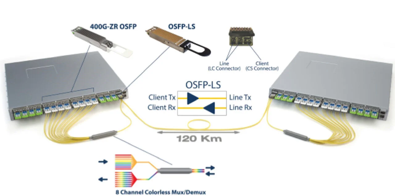
II-VI shrinks an optical line system into an OSFP module
II-VI has developed an optical line system that fits inside a pluggable module.
The advent of coherent pluggable modules implementing the 400ZR standard allows switches and routers to be linked across separate data centres. Now, with a pluggable optical line system, a dedicated line-system platform is no longer needed to send the 400ZR signals over a fibre.

Sanjai Parthasarathi
In turn, the network operating system on the switch manages the optical line system directly such that a separate optical management software is no longer needed.
“We have shrunk an entire pizza-box line system into a small pluggable,” says Sanjai Parthasarathi, chief marketing officer at II-VI.
Indeed, one customer refers to the II-VI pluggable product - dubbed the OSFP-LS - as a ‘zero-rack-unit’ platform.
Origins
A dense wavelength-division multiplexing (DWDM) system comprises transponders and an optical line system.
The elements used for a line system include an optical multiplexer and demultiplexer, amplifiers, and monitoring equipment that assess the quality of the DWDM link such as an optical channel monitor (OCM) and an optical time-domain reflectometer (OTDR).
Traditionally, a single vendor provided the optical line system and the transponders. Now line systems are ‘open’, part of the service providers’ demand to disaggregate equipment to avoid vendor lock-in. Accordingly, optical transponders from one vendor can now operate over another vendor’s line system.
II-VI supplies the components used for line systems: amplifiers, multiplexers and demultiplexers, OCMs, and OTDRs.
The idea of a pluggable optical line system came about following II-VI’s ongoing work to shrink the components used in line systems such as micro-pumps that are used in amplifiers. This requires not only shrinking the micro-pump but developing the required fibre and packaging technologies.
“We have been miniaturising and reducing the power consumption of pumps for years, primarily for embedded applications in transceivers,” says Parthasarathi.
Working with partners, II-VI has embedded its micro-pumps to fit within the CFP2-ACO and CFP2-DCO coherent modules.
“Knowing that 400ZR was coming and that it would use OSFP and other compact pluggables, and that many of the links will need amplification, we started looking at how our amplifier technology for the CFP2 could be shrunk further,” he says.
Networking equipment maker, Arista Networks, saw an ECOC 2018 Market Watch session given by II-VI and started a discussion.
Arista was interested in whether an entire line system pizza-box could fit in a pluggable. "That way, you wouldn’t require another box that needs to be powered and cooled,” says Parthasarathi. “That was the genesis of the idea.”
Parthasarathi says II-VI does not have an exclusive partnership with Arista but that the vendor is an early customer of the OSFP-LS.
OSFP-LS
Two amplifiers fit inside the OSFP: a booster amplifier used on the signal before transmission and a pre-amplifier at the receiver end. Uncooled micro-pumps are used so that no thermo-electric cooler is needed.

Sara Gabba
The multiplexing and demultiplexing circuitry is housed in the cabling, external to the module, and are II-VI custom designs.
Not everyone operating a data centre switch is skilled in optical engineering so the pluggable line system is designed to configure itself.
“It automatically detects the number of channels and sets the amplifiers, monitoring and adjusting them,” says Parthasarathi.
“A big part of the design is the implementation to optimise everything for this application,” adds Sara Gabba, strategic marketing manager at II-VI. “The gain-flattening and controlling the amplifiers’ power are technically demanding and therefore far from trivial.”
The current version of the OSFP-LS, supporting up to eight wavelengths, has been demonstrated by Arista to customers.
II-VI is looking to extend the pluggable optical line system architecture to higher channel counts thereby further exploiting a pluggable slot.
Source: Arista Networks
II-VI’s micro-pumps are rated above 400mW so amplifying 16 channels within a pluggable module is not an issue given that the power is shared across the channels.
As for multiplexing and demultiplexing more channels, II-VI is exploring using a separate cartridge as well as integrating the filtering functions inside the module.
The OSFP-LS will be generally available towards the end of 2020.
Future work
“400ZR is just the beginning,” says Gabba. “It will support the future 800G-ZR modules and can be adapted for other applications, wherever you need amplification and multiplexing-demultiplexing, including longer reach, cable, and mobile backhaul.”
The company is also looking to integrate the line system into the smaller QSFP-DD pluggable.
Extra features could also be added to the OSFP optical line system through further miniaturisation such as OCM and OTDR functions.
The initial module design uses photo-detectors for monitoring but does not have full optical channel monitoring. If a transceiver fails, the line system will continue to amplify the remaining channels but customers want to know if one of the wavelengths has gone down, says Parthasarathi.
After that, the only remaining feature is the reconfiguration of wavelengths. But Parthasarathi says the degree of miniaturisation needed is years off.
The majority of links data centre operators use are point-to-point; a pluggable reconfigurable optical-add drop multiplexing (ROADM) technology is not on their near-term wish list.

Ethernet Alliance on 800G and the next Ethernet rate
It may have taken the industry five years to get 400 Gigabit Ethernet (GbE) modules shipping, but for Mark Nowell, Advisory Board Chair at the Ethernet Alliance, the long gestation period is understandable given the innovation that has been required.

The industry has had to cram complex technology into a small form factor for 400GbE while meeting the requirements of two very different end-customers: webscale players and communications service providers.
400 Gigabit Ethernet
“The pressure is still on to get 400-gigabit out given that systems are shipping,” says Nowell. “Like with 100-gigabit QSFP28, it is always a rocky road at the beginning, getting all the reaches and getting all the [module] suppliers qualified.”
The 400GbE work is also continuing, with ICs for second-generation optics being tested in the labs that will reduce overall module power consumption.
Nowell notes the scale at which 400 Gigabit Ethernet will be adopted. The number of 400GbE modules expected to ship over the next five years will be 20x the 100GbE module units shipped during its first five years, based on forecast data from LightCounting Market Research.
“100 Gigabit Ethernet started very slowly because it was predominantly service providers [as adopters],” says Nowell. “What is happening with 400 Gigabit Ethernet is that now there is dual-demand from webscale players and service providers.”
This demand has pressured the industry in recent years to achieve a compact form factor, resulted in another noteworthy aspect of 400GbE. “400GbE is unique in that it is the first time we have come out with a new higher-speed Ethernet data rate where all of the reaches - from copper cables to coherent optics - fit in the same form factor,” says Nowell. “Unfortunately, we have two form factors: the QSFP-DD and the OSFP.”
The industry has also had to develop technologies such as 50-gigabit serialiser-deserialiser (serdes), with 100-gigabit serdes now following, and 100-gigabit-per-wavelength optics.
Creating working QSFP-DD and OSFP designs has also been a challenge; how to cool them and achieve the required signal integrity.
“This is the background to where we are today,” says Nowell.
800-gigabit pluggables
Two 800-gigabit multi-source agreements (MSAs) have been announced in the last year.
The 800G Pluggable MSA developing optical specifications for 800-gigabit pluggable modules, and the QSFP-DD800 MSA that extends the QSFP double-density form factor to support 800 gigabits.
The QSFP-DD800 MSA will ensure the connector supports 100-gigabit electrical signals and extend the module’s power envelope from 20W to 24W.
The QSFP-DD800 form factor will also be backwards-compatible with three other QSFPs: the 100-gigabit QSFP28, the 400-gigabit QSFP-DD and the 100-gigabit electrical input 400-gigabit QSFP400.
The first QSFP-DD800 MSA hardware specification was issued in March, to coincide with OFC. The release (version 1.0) has now been passed to the QSFP-DD MSA.
Nowell points out that the technology being used for 800-gigabit MSAs is the same as that being used for 400GbE.
“The amount of investment that we, as an industry, have put into getting these 400-gigabit building blocks, we need to recoup that,” he says. “We need to start building dense 400GbE, making more units and cost-reducing them; 800-gigabit pluggables will do just that.”
Thus, the same form factor - whether an OSFP or QSFP-DD800 - will deliver 2x400GbE or 8x100GbE. Accordingly, no 800GbE work needs to happen.
Next Ethernet rate
“What the 800-gigabit MSAs show is that there is a real interest in what is coming next,” says Nowell, who also co-chairs the QSFP-DD800 MSA.
Building 'denser 400-gigabit' in the form of 800-gigabit modules has an economic benefit for component vendors in that they can recover the investment they have made in the technology.
As for whether the network needs greater speed links, the reason is often one of two things, says Nowell. It either reduces the cost of networking or it benefits networking in terms of hashing efficiencies by using a higher capacity link.
“So does 800 Gigabit Ethernet need to exist to solve the hashing problem?” says Nowell. “I don’t hear a lot of people complaining about this being an issue.” And it would be the webscale players, given the scale of their operations, encountering this first, he says.
Nowell cites the emergence of co-packaged optics, whereby optics are added alongside an ASIC to provide the chip with high-speed optical input-output (I/O).
The requirement for co-packaged optics is coming from the cloud players and he cites the Co-Packaged Optics Consortium created by Microsoft and Facebook that issued a guidance document last year.
“They said this is what we need as an industry, and if you look at that, it is all based on dense 400 Gigabit Ethernet,” says Nowell.
The webscale players’ interest in co-packaged optic stems from the emergence of higher-capacity switch chips at 25.6 terabit and 51.2 terabits.
“The bandwidth demands that customers are seeing and the power efficiencies that customers are looking for, they need a roadmap of silicon development,” says Nowell. “The purpose of optics is to support the switch silicon.”
Adopting dense 400GbE will ensure that equipment using co-packaged optics will be able to talk to equipment using pluggables only.
Given work on 400GbE started around 2014, and that the capacity of Ethernet switch chips is doubling every two years, is there no urgency to define the next Ethernet rate?
Not yet, says Nowell, but it is something the Ethernet Alliance recognises.
It organises an event dubbed the Technology Exploration Forum (TEF) that brings together industry experts and the latest was scheduled for April 15th, focussing on the next Ethernet rate after 400GbE. However, due to the COVID-19 pandemic, the event has been postponed till October 7th.
“I don’t think there is any inconsistency yet but it is the right time to start, and that is why the Ethernet Alliance wants to drive the TEF event and have the discussion,” he says.
There is also the IEEE’s New Ethernet Applications group that acts as an incubator for new ideas. Such ideas can lead to a Call For Interest which, if sufficiently supported, is how new IEEE projects begin.
One such project that has just started is entitled Beyond 400 Gigabit that will look at market needs and define, from an IEEE perspective, what should be done in terms of technologies.
The IEEE 400GbE work took five years because it introduced several new technologies: 50-gigabit serdes, 100-gigabit-per-lambda optics, 4-level pulse amplitude modulation (PAM-4), and the use of 8-lanes for certain 400GbE implementations.
Nowell points out that the 800G Pluggable MSA includes 200-gigabit-per-lambda optics and FEC which are complex elements that require time to work through.
“My opinion is that if you want to do something in the IEEE, you want more headroom,” says Nowell. “It would be a mistake for the IEEE to only pursue 800 Gigabit Ethernet and then come up for air in several years and find that the industry has moved on.”
So the likelihood is that the next Ethernet rate will be at least 2.5x the current one (1TbE) and even as high as 4x (1.6TbE), similar to how 10GbE moved to 40GbE.
But this will be challenging, says Nowell. Issues such as what comes after 100-gigabit serdes and 100-gigabit-per-wavelength, and when will coherent technology be cost-effective enough for use within the data centre remain unresolved.
Meanwhile, the Ethernet Alliance’s TEF aims to shape the debate by bringing together different industry voices, with an emphasis on end-users and thought leaders.
Will the COVID-19 pandemic impede development and standards work?
“In this industry, we are used to working with collaborative tools so it’s not such a shock to pick up these to progress,” says Nowell. “I’ve been pleasantly surprised we have been able to do standards work this way without too much disruption other than it takes longer.”
But what is missing is meeting people face-to-face and the discussions that ensue.
“It does make a difference getting out and talking to customers,” says Nowell. “There is an unquantifiable thing that is missing.”

Nokia targets 400G era with PSE-V coherent DSP launch
Nokia has unveiled its latest coherent digital signal processor (DSP) family, its fifth-generation Photonic Service Engine dubbed the PSE-V.
Two devices make up the family: the high-end super coherent PSE-Vs and the compact PSE-Vc for use in pluggable modules.

Kyle Hollasch
The PSE-Vc chip is already sampling, the PSE-Vs will sample later this year.
The PSE-Vs, operating at a 90 gigabaud (GBd) symbol rate, supports transmission distances from local data centres to ultra-long-haul and sub-sea networks while the 64GBd PSE-Vc implements the OIF’s 400ZR standard, ZR+ and beyond.
Nokia has also expanded its coherent optics strategy having completed the acquisition of Elenion Technologies. It is now vertically integrated and is offering coherent optics and its DSPs to partners that include module makers and contract manufacturers.
The 400G era
The last decade has been primarily based on 100 gigabit, with 100-gigabit client signals appearing around 2010 and coherent optics starting at 100 gigabit. “We like to forget about 40 gigabit,” quips Kyle Hollasch, director of optical networking product marketing at Nokia.
This decade marks the start of the 400-gigabit era. “Just about this year and, in earnest, next year, we will see 400 gigabit adopted as the dominant data centre client-rate, timed along with 400-gigabit coherent,” says Hollasch.
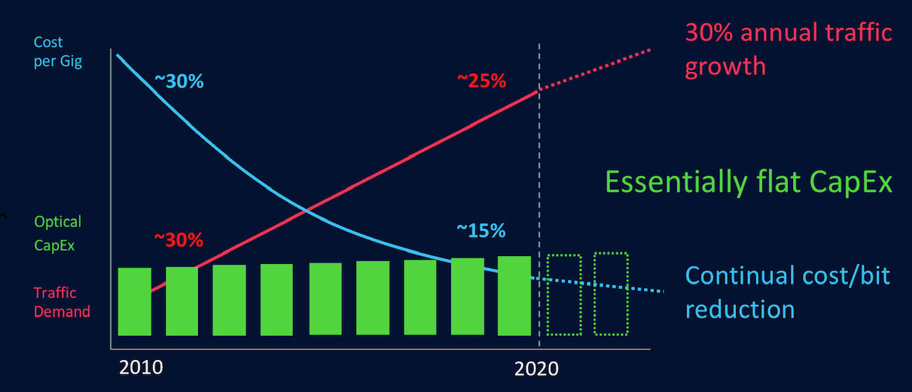
During the last decade, traffic has continued to grow exponentially while cost-per-bit has declined, first at 30 per cent per annum and more recently at 15 per cent. Overall, the optical market spend has been largely flat over the last decade (see diagram).
Meanwhile, the technologies underpinning coherent and optical transport are becoming more challenging.
Optical performance using coherent has improved significantly with advances in baud rate, modulation schemes and forward-error correction (FEC). So much so that optical performance is approaching the theoretical Shannon limit. “We don’t know where it is but we know we are close,” says Hollasch.
Moore’s law is also slowing down. The gains in processing performance and power reduction are harder to achieve with each advance in CMOS process geometry. The latest PSE-V devices are implemented using 7nm CMOS.
“The question we are trying to answer is that, with this new era and certain technology trends slowing down, how are we going to keep scale and cost-containment going,” says Hollasch.
Coherent strategy
Nokia highlights three elements to address scale and reduce cost.
In addition to its existing coherent DSP expertise, Nokia has added an optical engine design capability, and integration and packaging know-how.
The CSTAR optical engine, gained with the Elenion acquisition, includes silicon-photonics-based optics and transmitter and receiver ICs that are parcelled in a BGA chip package
“The existing CSTAR portfolio is already shipping to several customers and there is a lot of development and opportunities going forward,” says Hollasch.
The PSE-Vc and the optical engine are being integrated into various form factors to deliver different price points and optical performances. “And the market is rapidly shifting towards pluggable [coherent] transceivers,” says Hollasch.
Being vertically integrated brings cost-advantages, says Hollasch, as well as an ability to innovate faster by ‘owning’ the entire development and manufacturing process.
The approach has been adopted by other optical transport companies. Infinera has always developed its DSPs and indium-phosphide optics; several years ago Ciena brought indium-phosphide and silicon photonics expertise in-house to complement its DSPs, Huawei also has both DSP and optics expertise, while Cisco Systems gains both with its Acacia acquisition.
Nokia’s partners will be its customers, using its components and taking the resulting products to market. In turn, Nokia will also be a customer of modules and subsystems.
“Elenion was a corporate acquisition,” says Hollasch. “It lives under the optical unit but it was acquired for the benefit of the entire corporation.” After the optical unit, Nokia’s IP division will be the next largest consumer of transceivers, particularly at 400 gigabit, while mobile and access “are at the cusp of coherent adoption”, he says.
Hollasch does not rule out its modules being sold via partners and resellers: “It is still early in the process but it is absolutely part of the roadmap.”
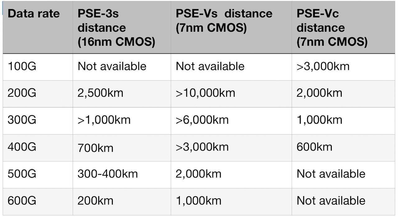
PSE-Vs
Upping the symbol rate of the PSE-Vs to 90GBd delivers a significant performance benefit.
In the current-generation PSE-3, 400-gigabit transmission at 64GBd requires 16-ary quadrature amplitude modulation (16-QAM) whereas operating at 90GBd, quadrature phase-shift keying (QPSK) can be used.
“Instead of a regional distance of 1,000km [for 400-gigabit 16-QAM], you can send QPSK almost anywhere on the planet,” he says (see table).
The PSE-Vs is Nokia’s second-generation DSP to use probabilistic constellation shaping (PCS). The technique allow the transmission data rate to be defined with fine granularity, tailored for a specific link. Nokia was the first vendor to implement PCS with its PSE-3.
The 90GBd baud rate is used for all the data rates, from 200-600 gigabits-per-second (Gbps) using PCS. A reach of 1,000km is possible at 600Gbps whereas 200Gbps is used to address the longest sub-sea spans.
Hollasch highlights what he believes is a key benefit of Nokia’s technology: the joint optimisation of PCS and its proprietary FEC scheme.
Hollasch says its FEC reduces the extra bits that are appended to the data - the overhead payload - from 25 per cent to 16 per cent: “We believe that gives a performance enhancement not available to the rest of the market.”
Nokia says silicon photonics and indium phosphide will be used for PSE-Vs-based coherent designs.
“We believe that we can achieve similar performance with both technologies,” says Hollasch. “The reason for using both is for diversification of supply; the COVID-19 event has shown that we need diversification in all areas of our supply chain.”
Source: Nokia, Gazettabyte
PSE-Vc
The PSE-Vc will be used to implement 400ZR and ZR+ in a QSFP-DD pluggable module.
Nokia refers to the two extremes of coherent, as exemplified by the ‘super coherent’ and ‘compact’ names for its PSE-V chips, as high-end performance and profile, by which it means form factor.
Whereas performance is all about maximum reach and reducing cost/bit/km, profile is concerned with cost, interoperability and being pluggable.
But Hollasch stresses there is an important middle region where the goal of the interfaces - partly the ZR+ and the rest the CFP2-DCO - is to balance these two extremes.
“The middle does not get the attention; all the attention goes to the high-end,” says Hollasch. “But the vast majority of optical networking is happening in the middle.”
Nokia is implementing 400ZR and ZR+ using the QSFP-DD form factor. ZR+ extends the performance of 400ZR by supporting traffic protocols other than Ethernet as well as data rates of 400 gigabits and below. Such rates - 100 to 300 gigabits - extend reach beyond 400ZR’s 120km.
Nokia is not adopting the OSFP form factor for coherent. “We don’t see a huge demand for the OSFP,” says Hollasch.
The CFP2-DCO using the PSE-Vc is what Hollasch refers to as the ‘ZR++’. The greater volume and power envelope of the CFP2 module means its optical performance can exceed greatly that of 400ZR and ZR+. “The CFP2 will be a large part of our optical platforms.”
The CFP2 and the QSFP-DD modules will be available towards year-end.
No 800 gigabit
Unlike its rivals Ciena, Huawei and Infinera, Nokia has chosen not to support 800-gigabit wavelengths with its latest high-end DSP.
The company argues that at data rates greater than 600 gigabit, the reach is limited. “It is not that 800 gigabit isn't important, it is just that it lives in a world of many options,” says Hollasch.
The 800-gigabit rate is not economical to pursue with this generation, he says: “For data centre interconnect, it is much more economical to pursue shorter distances with 400ZR and ZR+.”
He argues that 400-gigabit coherent pluggables will be hard to beat in terms of power consumption and cost, given the demand from the webscale players and the many companies making them. Equally, since 400ZR is a standard, modules are interoperable.
Nokia also highlights the engineering issues involved in implementing rates above 600 gigabit.
At 600 gigabit, the PSE-Vc uses 16-QAM whereas 800 gigabit requires 64-QAM. Processing four times as many constellation points loads the DSP for what is a limited use case. “It puts lots of strain on the DSP; we know, we did 64-QAM in both the PSE-2 and PSE-3,” he says.
Confining an 800-gigabit wavelength to a 100GHz channel limits its reach to 100-200km, says Hollasch. Extended the channel to 125GHz, the reach of an 800-gigabit wavelength is extended. But two 400-gigabit pluggables, each using a 75GHz channel, can also be used to transmit the same capacity over long reaches.
In other words, a 125GHz channel is needed ‘to get anywhere’ while saving very little in terms of spectral efficiency, concludes Hollasch.

NeoPhotonics talks 400ZR, 600G, 800G and Lidar
Many companies that prepared for the OFC show in March had their plans thwarted due to the COVID-19 pandemic.
OFC did take place in San Diego despite all the hardships. But company withdrawals meant technology demonstrations were scrapped, press releases went unissued and stories left untold.

Ferris Lipscomb
Intel and Ranovus, for example, planned to fanfare their first co-packaged optics designs at OFC. Demonstrations to interested parties did occur but at their offices instead.
Equally, 800-gigabit coherent technologies from Ciena and Infinera would have been showcased at the show, as would industry organisations' interoperability demonstrations.
NeoPhotonics announced in January that it was sampling 400-gigabit coherent pluggable offerings in the CFP2 and OSFP form factors.
At OFC, NeoPhotonics was to show a QSFP-DD module implementing the 400ZR OIF coherent standard, thereby completing its 400-gigabit coherent portfolio.
“A lot of the planned demos involved interoperation in customer switches with other modules,” says Ferris Lipscomb, vice president of marketing at NeoPhotonics. “Many of these demos are now being done in San Jose [its HQ in California] for customers coming individually.”
Chip-stacking and 400ZR
NeoPhotonics’s 400ZR QSFP-DD module is also now sampling.
Acacia Communications has said how it is using 3D-chip packaging technology for its 400-gigabit coherent module designs. Acacia assembles the module’s components - the coherent digital signal processor (DSP), the silicon-photonics photonic integrated circuit (PIC), and the modulator driver and trans-impedance amplifier (TIA) - into one package using chip-stacking techniques.
Is NeoPhotonics doing something similar with its coherent pluggables?
“That has been the end-game for some time and will provide the ultimate size and performance,” says Lipscomb. “But I don’t think 400ZR is the point where it is needed.” The expected volumes for 400ZR modules, while large, will be in the couple of hundred thousand units.
Instead, the “tried-and-true” technology of the COSA and optics, integrating the TIA and driver, along with a separate DSP, does the job for this generation, he says. A coherent optical sub-assembly (COSA) combines the interdyne coherent receiver and the coherent modulator driver (CDM).
Since the DSP generates the most heat within the module, the separation helps disperse the DSP’s heat from the other components.
“We think that when you start to use coherent inside the data centre, and for shorter reaches and higher speeds, such [3D] packaging makes sense and that is where it will end up,” says Lipscomb.
High-bandwidth coherent driver modulator
NeoPhotonics announced the general availability of its high-bandwidth coherent driver modulator (HB-CDM) to coincide with OFC.
The device, operating at a symbol rate of 64 gigabaud (GBd), comprises a quad-channel driver and an indium-phosphide-based quad modulator.
Used alongside NeoPhotonics’s 64GBd interdyne coherent receiver and its narrow linewidth tunable laser, the HB-CDM supports data rates up to 600 gigabit-per-second (Gbps).
At 600Gbps, 64-ary quadrature amplitude modulation (64-QAM) is used and the reach is 80km, suitable for data centre interconnect. At 400Gbps using 16-QAM, metro distances of between 400km and 600km are possible, while at 200Gbps the reach achieved is over 1,000km.
The company also has a 64GBd C++ HB-CDM variant that supports the ‘super-C band’ that extends transmission capacity by using 50 per cent more fibre spectrum than the standard C-band; 6.4THz in total.
Lipscomb says that the HB-CDM design will also support 800Gbps using a symbol rate of 96GBd. "We have not announced general availability of the 96GBd [HB-CDM] but we do it," says Lipscomb.
Other coherent uses
NeoPhotonics is applying its coherent optics know-how for non-communications applications such as Lidar, 3D-sensing and medical diagnostics.
A Lidar system uses light from a laser to sense its environment and can be used as one of several sensors to enable self-driving vehicles.
Earlier this year, the company announced that it was sampling high-power semiconductor optical amplifiers (SOAs) and narrow linewidth distributed feedback lasers (DFB) for automotive Lidar applications. The devices operate at 1,550nm and enable automotive Lidar systems to scan distances beyond 200 meters.
As has happened in optical communications, Lidar systems are evolving from on-off keying - pulse modulation - to coherent detection, says Lipscomb. This boosts sensitivity as the use of a local oscillator acts as an amplifier.
“Any time you need higher sensitivity in optical measurement, coherent is advantageous,” says Lipscomb. “With coherent detection, you can measure things with much higher accuracy and much lower power because you are looking at the phase rather than just, as with a lot of Lidar systems, counting the photons that bounce back.”
Using a coherent-based Lidar, the range and velocity of objects can be sensed. The transmitted frequency of the laser - represented by the local oscillator - and the reflected signal are mixed coherently. This enables phase and amplitude information to be recovered to determine an object’s position and velocity.
The sensing work is at the development stage rather than running businesses but NeoPhotonics is already working with several systems companies.
800ZR
Given the OIF has just published the Implementation Agreement for the 400ZR coherent optical interface and the first 400ZR module products have been announced, what next for coherent pluggables?
The answer is the same OSFP and QSFP-DD form factors implementing 800-gigabit coherent, says Lipscomb.
Such 800-gigabit modules will require co-packaging of the DSP, the optics and associated circuitry. The DSP will also need to be implemented using a 5nm CMOS process node.
Accordingly, such products are likely to be at least three years out. “There is a lot of discussion about it but it is on everyone’s roadmap,” says Lipscomb.
Another goal is the use of coherent technology within the data centre.
“Right now, for 40-80km and above, coherent is a cost-effective solution but inside the data centre it is all PAM-4,” says Lipscomb. “But as the cost of coherent decreases and speeds get higher, you get more of an advantage, and that distance will get shorter.” PAM-4 refers to 4-level pulse-amplitude modulation.
Ranovus outlines its co-packaged optics plans
Part 2: Odin technology
Ranovus has tested a chiplet that combines electronics and silicon photonics. Dubbed Odin 8, the monolithic design is targetting the co-packaged optics opportunity, enabling silicon chips to communicate optically.
The company is developing two such chiplets: the 800-gigabit Odin 8 and the higher-capacity Odin 32 that supports 3.2 terabits of traffic.

Hamid Arabzadeh
The first use of Odin 8 will be for 800-gigabit client-side modules. “We already have three lead customers for our 800-gigabit module business,” says Hamid Arabzadeh, CEO of Ranovus.
The 800-gigabit pluggable modules using the Odin 8 are expected to be generally available from late 2021.
Company
Founded in 2012, Ranovus is a late-stage start-up that has raised close to $100 million in funding. About half the sum is from venture capital firms and the rest is non-dilutive funding from sources including the Canadian government. An unnamed strategic investor also closed a deal with Ranovus late last year.
Ranovus has several core technologies including a multi-wavelength quantum-dot laser, a silicon photonics-based ring resonator, and driver and receiver electronics.
Ranovus is bullish about its ring-resonator - used for modulating and filtering light - and claims to own core intellectual property (IP). “We have spent a lot of time over the last eight years patenting quite a lot of the key fundamentals,” says Arabzadeh.
The first product Ranovus developed addresses the data centre interconnect market. The 200-gigabit direct-detection CFP2 pluggable module uses four wavelengths, each at 50 gigabits, and has a reach of 85km.
But looming competition from 400ZR, the OIF 400-gigabit coherent standard for data centre interconnect, caused Ranovus to shift strategy a couple of years ago and develop products for use within the data centre. To this aim, the company bolstered its team with senior management appointments.
Data centres
Ranovus’s Odin co-packaged optics solutions are aimed at servers and Ethernet switches deployed in data centres.
Machine learning and artificial intelligence are fueling traffic growth placing new demands on servers.
“GPUs, CPUs, memory and storage are configured using electrical interfaces, and the higher bandwidth requirements will eventually lead to optical interfaces,” says Arabzadeh. A graphics processing unit (GPU) is a class of processor suited to machine learning. Such chips are sold by companies such as Nvidia, AMD and Intel.
Server are also adopting a disaggregated design whereby the elements needed for computation - processing, memory and storage - are pooled separately. This addresses the changing nature of workloads and allows for the server components to be upgraded independently.
“If you look at workloads in the cloud, these differ,” says Arabzadeh. “Some require a lot of processing, others need a lot of memory accesses. So this entails moving to pooled compute, pooled memory and pooled storage; a monolithic server doesn’t meet all the needs.”
Arabzadeh cites as an example the Open Compute Project’s (OCP) Open Accelerator Module (OAM) that combines eight GPUs. GPUs work on tasks that are highly latency- and protocol-sensitive.
Each GPU has an electrical bus to connect to storage and memory and there are lots of communication between GPUs and between GPUs in different racks, says Arabzadeh. As speeds go up, any hop between GPUs has to be optical because electrical links won’t be able to support that.
“Our Odin platform - our biggest claim to fame - is its low latency of 0.4ns,” says Arabzadeh. “We have validated this with four major systems players and we have tested their devices with our product and shown that this latency doesn't impact any of the protocols they use.”
The second key market for co-packaged optics is data-centre networking. Here, Ethernet switch chip capacities are doubling every two years.
Last December, Broadcom started delivering its 25.6-terabit StrataXGS Tomahawk 4 switch-chip, while the Barefoot division of Intel has spoken of its 25.6-terabit coming soon and has hinted that its 51.2-terabit switch chip is close behind (see Part 1: Intel combines optics to its Tofino 2 switch chip)
A doubling in switch-chip capacity requires a doubling of input-output (I/O) where ever-faster signals need to go across a printed circuit board. This is both a design challenge and burns power. Bringing optics alongside the switch chip allows shorter-reach XSR serialiser-deserialisers (serdes) to be used, saving power.
Odin devices
The Odin 32 device comprises silicon photonics-based optics and driver, receiver and control electronics.
The electrical inputs to the Odin 32 are 100-gigabit 4-level pulse-amplitude modulation (PAM-4) signals while the optical output uses eight fibres, each carrying a 400-gigabit FR4. Each FR4 is made up of four, 100-gigabit wavelengths.
The laser used is external to the Odin 32 since the chiplet’s temperature and power dissipation is quite high. “Using an external laser is compliant with what Facebook and Microsoft have launched in their co-packaged optics document,” says Arabzadeh.
Ranovus has developed a socket-based design such that each Odin 32 device surrounding the ASIC can be easily clipped on and removed. Using 16 such Odin 32s delivers the I/O needed for a 51.2-terabit capacity switch chip (see photo below).
A co-packaged design: 16 chiplets providing optical I/O for the silicon chip. Source: Ranovus
The Odin 8 uses a similar design except the laser is integrated internally with the silicon-photonics and electronics.
For 800-gigabit pluggables, a PAM-4 chip is also used. Ranovus is working with two PAM-4 suppliers to co-package the PAM-4 chip with the Odin 8 device. “The optical engine, laser and the PAM-4 chip are all inside,” says Arabzadeh.
The company was going to demonstrate the Odin 8 implementing FR8 - sending eight 100-gigabit wavelengths on a single fibre - at the recent OFC show held in San Diego in March. But that was cancelled due to the COVID-19 pandemic.
Ranovus is targeting the 800-gigabit DR8 as its first market. “We see a market pull for the DR8 for 800 gigabits,” says Arabzadeh.
Addressing pluggables first with Odin 8 reduces the risk to end-customers keen to adopt the novel technology. “They can kick the tires on it, and then co-packaged optics will be a natural progression,” he says.
Pursuing both co-packaged optics and pluggable solutions also caters for the differing preferences of large-scale data centre players. Facebook and Microsoft are promoting co-packaged optics but at OFC both Google and Alibaba highlighted their preference for pluggable optics due to their flexibility and ease of use.
Cost and power
Ranovus says its co-packaged optics design halves the power consumption and reduces by three-quarters the cost of 100-gigabit pluggable modules.
Assuming a 100-gigabit module consumes 3-3.5W and costs $150 to $200, that implies the 3.2-terabit Odin 32 consumes between 48-56W and costs between $1,200 and $1,600.
The CEO holding the multi-chip package, highlighting its size. Source: Ranovus.
One-hundred-gigabit modules rather than 400-gigabit modules were used for the comparison since 400-gigabit pluggables have yet to reach volume production. Accordingly, their pricing hasn’t stabilised nor has the power consumption had time to progressively come down.
“With the emergence of 100-gigabit serdes on switch ICs, we see the life of 400-gigabits, with 50-gigabit electronics going to 100-gigabit-per-wavelength, as being very short,” says Arabzideh. “We don't think they will reach critical mass in terms of power consumption and getting the cost down.”
Drivers for co-packaged optics
Ranovus, along with IBM, TE Connectivity and Senko Advanced Components, have formed a consortium to help firms embracing co-packaged optics to design and manufacture their products.
IBM brings its V-groove technology that is used for connecting fibre to the optics while TE Connectivity has worked with Ranovus on the packaging and the clip mechanism that fix in place the engines around the ASIC. Senko Advanced Components’s contribution is the design of the connector technology.
So what will trigger the adoption of co-packaged optics in the data centre? Arabzadeh cites three factors that will spur the technology’s introduction: power consumption reduction, miniaturisation and cost savings.
A key contributor to power reduction is the advent of 100-gigabit electrical interfaces so that, at last, the electrical signal rate matches 100-gigabit wavelengths.
The electrical input signalling rates have continued to lag behind pluggables’ 100-gigabit optical outputs. The advent of 100-gigabit electrical interfaces now means no rate-translation or ‘gearbox’ chip is needed, and that saves power.
“It becomes an electro-optic conversion without any multiplexing,” says Arabzadeh. “This is a key factor for co-packaged optics to be enabled.”
The second driver is systems miniaturisation. One parameter that is fixed is the upper size of switch chips. There is a certain die size above which yields start to go down. So the dimensions of the die will remain fixed with the move from 25.6-terabit to 51.2-terabit switch chips.
One issue that will help the design is the move from a 7nm to a 5nm CMOS process - allowing more transistors to be crammed in the fixed area. But each CMOS process shift is harder to achieve and is more costly.
But the issue remains getting the I/O signals off the chip to the front panel where the pluggable optics reside. For a 51.2-terabit switch chip, that is challenging.
The fixed size of the chip means the ever-higher-speed signals need to fan out from the chip to the very edges of the front panel. “This is going to be a nightmare; you are going to have retimers [chips] everywhere,” says Arabzadeh. By bringing the optics closer to the switch chip using co-packaged optics, the fan-out is lessened as the distances become shorter.
There is also the expectation that, given the size and number of the pluggable modules needed, a 51.2-terabit design will not fit into a one-rack-unit (1RU) platform. Using co-packaged optics, a 1RU 51.2-terabit switch is possible.
“There is a physics issue here: miniaturisation and not being able to fan out,” says Arabzadeh.
The third factor pushing towards co-packaged optics is cost reduction, argues Arabzadeh, pointing to Ranovus’s monolithic chiplet design: “The transistors are designed in the same mask as the silicon photonics”.
This means no wire-bonding is needed between the optics and separate electronics ICs, implemented using silicon germanium or CMOS.
“Each of these interfaces has to be optimised on an analogue level,” he says, adding that these factors increase the cost and power consumption. In contrast, a monolithic design means wafer-scale manufacturing can be used which benefits the economics.
“It is something we think will be cost-effective inside the data centre,” says Arabzadeh.
Availability
Engineering samples of the Odin 8 are expected in the first quarter of 2021, while general availability of 800-gigabit DR8 pluggables using the chiplet is due towards the end of next year.
But the timing is also dependent on the availability of PAM-4 chips. “There are not too many PAM-4 chips at 800 gigabits,” says Arabzadeh. The first PAM-4 designs so far announced use 7nm CMOS and despite that being state-of-the-art, Arabzadeh says lower-power chips are needed.
Meanwhile, the Odin 32 will tape-out in the third quarter of this year.
As for co-packaged optics, that is expected some six months to a year after 800-gigabit modules, says Ranovus: the second half of 2022.
How We Rethink Our Approach To Daily Commitments
Many years ago, I worked for my parents who own a video production company. Because it is a family business, you inevitably end up wearing many hats and being the czar of many different jobs. I mainly managed projects and worked as a video editor. On production, there were times that I was called on to work as an audio tech and was made to wear headphones on long production days. In those days, having a really good set of headphones that picked up every nuance of sound was essential to making sure the client got what they needed. Naturally, my first impression of these headphones is based off of the look of them. They have a classic over-the-ear style that is highlighted by a blue light that indicates the power for the noise canceling. The padding on the ear pieces seems adequate for extended usage periods.
They are wired headphones, but the stereo mini-plug cable is detachable. Something else I noticed right of the bat was the very nice carrying case that comes with them. It has a hard plastic exterior with a soft cloth interior that helps to protect the surface of the headphones from scratches. I never truly appreciated cases for headphones until I started carrying them from place-to-place. Now I can’t imagine not having a case. Once I gave the headphones a thorough once-over exam, I tried them on. As I mentioned, they have a classic over-the-ear style and just looking at them, the padding on the ear pieces seem adequate and the peak of the headband seemed to be a bit lacking, but you don’t really know comfort unless you try on the product. So, I slipped the headphones on and found them to be exquisitely comfortable.
If you look at what you have in life, you'll always have more. If you look at what you don't have in life, you'll never have enough.
Oprah Winfrey
Now that I had the headphones on my head, I was finally ready to plug and play some music. I plugged the provided cable into the jack on the headphones and then the one on my iPhone. Then I called up Pandora. I tend to have a very eclectic music purview and have many stations set up for different moods. the sound quality of these headphones was remarkable. There is an amazing depth of sound and incredible highs and lows that make listening to music a truly breathtaking experience. In order to test how voices sounded, and the overall art of mixing, I pulled up Netflix on my iPad Air and watched a few minutes of a movie to hear all the nuances of the film.
None of them were lost. In fact, I ended up hearing sounds that I hadn’t heard before. Echoes…birds chirping…wind blowing through trees…breathing of the characters…it was very impressive what the headphones ended up bringing out for me.
