
Books in 2020
Each year Gazettabyte asks industry figures to pick their reads of the year. Industry analysts and regular contributors Dana Cooperson and Andrew Schmitt kick off this year's highlighted books.

Dana Cooperson, independent analyst
I had difficulty concentrating enough to read during the lockdown despite having more time. Eventually, events spurred my overdue fiction/ non-fiction exploration of the underpinnings of systemic racism as well as some escapism through journeys that the pandemic made impossible.
Five of my books fit the first category: four explore the legacy of human slavery in the US and the African-American experience, while the fifth, Trevor Noah’s memoir, traces similar terrain in apartheid/ post-apartheid South Africa.
Just Mercy: A Story of Justice and Redemption by the lawyer and equal justice advocate, Bryan Stevenson, uses statistics and egregious cases of the miscarriage of justice that lead to the unequal application of capital punishment.
Stevenson intersperses the shocking case of Walter McMillian, a young, self-sufficient Black man who was wrongly accused of killing a white woman, with tales of his founding of the Montgomery, Alabama-based non-profit Equal Justice Initiative (EJI), and a procession of cases EJI litigated on behalf of poor, minority, and juvenile clients.
One wonders how Stevenson and his team could work doggedly on these cases while facing death threats and obstacles. There are few happy endings for the accused yet the book is ultimately hopeful.
The Warmth of Other Suns: The Epic Story of America's Great Migration by journalist Isabel Wilkerson is a history of the migration of six million African Americans from the agrarian Jim Crow South to the urban north and west of the country between 1915 and 1970.
The book weaves broad historical and sociological data with the bittersweet stories of three individuals who migrated to escape terrorism and lack of opportunity. It also helped me piece together historical underpinnings of today’s fight for justice, as epitomised by the Black Lives Matter movement.
If the statistics don’t move you, the stories of Ida Mae Brandon Gladney, George Swanson, and Robert Joseph Pershing Foster will. (Note: Wilkerson recently published a follow-up, Caste, which my reading buddies recommend.)
James Baldwin’s Go Tell It on the Mountain is a semi-autobiographical novel about an African-American boy growing up in 1930s Harlem. This beautifully written, structurally interesting book focusses on fourteen-year-old John, who is struggling with poverty, abuse, and religious faith; and John’s father, Gabriel, mother Elizabeth, and Aunt Florence, all of whom escaped Jim Crow and who all struggle. Baldwin writes with imagery and passion. I had not read Baldwin before.
This year I also returned to Tony Morrison, with Sula, another tale of African-American diaspora that begins in 1919 Ohio. Like Baldwin’s book, Sula deals with intergenerational trauma and features indelible characters and powerful prose. A slim book, deep in characterisation and emotional punch.
A no less passionate book, infused with its author’s gift for making people laugh, is comedian Trevor Noah’s memoir, Born a Crime: Stories From a South African Childhood.
The book’s title refers to South Africa’s Immorality Act of 1927, which made his birth by a black Xhosa mother and white Swiss father in the waning days of apartheid punishable by five years in prison.
The book details the hoops his family jumped through to avoid incarceration during apartheid and Noah’s chameleon-like abilities to navigate South Africa’s bizarre race-based caste system and a thriving black-market economy.
A polyglot, Noah’s facility with languages was key to his ability to navigate situations, some of which were life-and-death serious.
Rounding out this year’s recommendations are four excellent books that took me to different times and places.
The Awakening, published in 1899, deals with protagonist Edna Pontellier’s search for meaning and escape from the strict social customs of nineteenth-century New Orleans society.
The book, which treats adultery unapologetically, created such a backlash against author Kate Chopin that she stopped writing. My daughters, who read the book in school, tipped me off to this classic. The ending, which I won’t spoil, leaves one wondering whether this a feminist tale and the ending's meaning.
If you are looking for a diverting read, you can’t do better than something— anything— by Bill Bryson. Bryson is an Iowa-born journalist and author who ruminates on such topics as language, culture and history.
This year I read Bryson’s At Home: A Short History of Private Life which uses the Victorian parsonage where he lived in “a part of England where nothing of any great significance has happened since the Romans decamped” to anchor a room-by-room history and cultural reflection on the evolution of private life.
His writing roams across ten thousand years of history, etymology, and sociology, such as how the “hall” evolved from the most important room in a domicile to “a place to wipe feet and hang hats” and how “limelight” became associated with the theatre.
Circe by Madeline Miller is a retelling of Homer’s The Odyssey from the perspective of the titular sorceress, who is banished by Zeus to a remote island. Confusing at first, the novel is ultimately rewarding for those interested in mythology. Spoiler alert: Odysseus does not fare well in this version of the tale.
News of the World by Paulette Giles is a sweet little book "soon to be a major motion picture" starring Tom Hanks.
The book is set in the aftermath of the US Civil War in 1870s Texas. Septuagenarian war veteran, Captain Jefferson Kyle Kidd, is an honourable man who makes his living travelling to towns and charging a fee for reading newspapers from around the world. He agrees to take a young German orphan girl, who has been recaptured (and questionably “liberated”) from the Kiowa tribe that killed her parents, to her relatives 400 miles away. What is the right path for the Captain and his charge? Don’t wait for the movie to find out.
Let’s hope 2021 is a better year for all.
Andrew Schmitt, founder and Directing analyst at Cignal AI
I was told The Bitcoin Standard was the book to read to get a perspective on the technology. It is indeed a good book though heavily biased in favour of bitcoin and against the global government fiat money scheme. It keeps the politics in the background and is a good primer to understand what is supposedly happening with Bitcoin.
I re-read Dune by Frank Herbert in anticipation of the new movie after first reading it decades ago. It's a great book but requires investment, and the payoff is just entertainment. I never read the sequels after reading the first book and I don't want to now.
In American War by Omar El Akkad, a future America is torn by civil war due to climate change. The book was recommended to me; I can't recommend it myself. I'm just not into bleak disaster themes anymore. It will probably become another Netflix series.
I also re-read The Good Shepherd by C. S. Forester in anticipation of the movie that was never generally released. I read it when I was young; I don't remember why. It's well-written and now I want to look at his other works.
I ended up seeing the movie on AppleTV, which tried to capture the captain's deep thinking that the book expresses so well. But this was a battle fought in the captain's mind and you need to read the book to see it correctly.

Broadcom’s 14.4-terabit Jericho2c+ router chip
The inexorable growth of IP traffic is being driven by ever more powerful devices being connected to the network and greater numbers of machines talking to each other.
In turn, Covid-19 has contributed its own traffic spike: AT&T reported that in September its core network traffic was 20 per cent up compared to March’s figures.
Jericho2c+ architecture. Source: Broadcom
The growth means that each new generation of router platform must at least double the traffic throughput while keeping the power consumption fixed.
This is a considerable challenge but one that the router chip designers continue to meet.
Jericho2c+
Broadcom announced recently its 14.4-terabit Jericho2c+ chip that increases router capacity threefold compared to the Jericho2c.
The Jericho2c+ is Broadcom’s third Jericho2 chip in just two years, samples of which are now with customers. Broadcom says the device should be qualified by year-end.
“The surprise is the generational cadence Broadcom is maintaining for the Jericho line,” says Bob Wheeler, vice president of The Linley Group and principal analyst for networking. “They remain committed to leading in chassis-based switch and router designs.”
Jericho2, a 9.6-terabit chip aimed at data centre router applications, was announced in 2018. The 4.8-terabit Jericho2c followed a year later, a derivative targeting the service-provider market.
Now, the Jericho2c+ triples throughput using a 7nm CMOS process instead of a 16nm used for the Jericho2c and has enabled Broadcom to boost the on-chip cores’ clock frequency.
“From an architecture standpoint, Jericho2c+ is an evolution of Jericho2, not Jericho2c,” explains Wheeler. “But yes, for Jericho2c customers, J2c+ does triple throughput.”
Router trends
Oozie Parizer, senior marketing director, Broadcom, says the company has played an important role in the telecom operators moving from router platforms using custom ASICs to platforms using merchant silicon.
“Recently we see more of this transitioning, not just to merchant silicon but also to white boxes,” says Parizer. This transition applies to core and edge routers.
“It has been possible because of the availability of merchant silicon to all, enabling a different price structure,” says Parizer. “All the OEMs are designing platforms; at the same time, some are maintaining their own [router] ASIC designs.” Router vendors developing ASICs include Cisco Systems, Juniper Networks and Nokia.
Telecom operators are keen for the established router vendors to use merchant silicon, says Parizer: “The carriers are buying into this story because they see what happened in data centers 10 years ago [with switching silicon].”
Wheeler sees a role for both custom ASICs and merchant silicon.
“The leading router OEMs remain committed to ASICs for their core routers; these are “halo” products meant to lead in features rather than being cost efficient,” he says. “Meanwhile, many of these same OEMs use Jericho for higher volume routers and transport platforms.”
Jericho architecture
The 14.4 terabit-per-second (Tbps) Jericho2c+ splits its interface capacity with 7.2Tbps facing the front panel and 7.2Tbps to Broadcom’s accompanying fabric chip, dubbed the Ramon. The Ramon is a cell-based switch chip that features 192, 50-gigabit serialiser/ deserialisers (serdes).
The fabric interface of the Jericho2c+ is indeed 9.6Tbps, the extra 2.4Tbps used for redundancy. “This is a carrier-grade system; they care about robustness,” says Parizer.
Should a line card fail, traffic is routed to a spare card to ensure continued traffic flow. The spare card may cover three working cards, but systems also use higher ratios: a spare card for every five, seven or even nine cards.
The Jericho2c+ has added on-chip security. “We have integrated MACSec and IPSec at line rate for all the network interfaces of the Jericho2c+,” says Gadi Singer, principal product manager at Broadcom.
Hyperscalers and service providers want to secure communications beyond their premises and integrating security hardware on each port reduces system cost and overall power consumption, says Singer.
Implementing a 14.4Tbps router with security and redundancy using two Jericho2C+ devices halves the power of a similar capacity platform using the Jericho2c. Such a design requires 21 chips: three Jericho2 ICs and the rest security ICs.
The Jericho2c+ doubles the number of meters while supporting more queues than previous Jericho devices. Meters and queues are used to enforce quality-of-service schemes to prioritise traffic flows and services.
“We wanted to ensure that even for the most demanding cases, we have sufficient meters and queues,” says Parizer.
The chip also features two stacked high-bandwidth memory (HBM) for packet buffering; 8 gigabytes of high-speed store in total.
Programmable pipeline
The Jericho devices feature a programmable pipeline.
A set of known features can always be implemented more efficiently with dedicated hardware; extra logic is needed to make the pipeline programmable. But a programmable pipeline can support different use cases. “You future-proof it for something that might come up after you design or even deploy the chip,” says Parizer.
The Jericho2c+ includes parsers and special function units for both the pipeline’s input and output paths.
There are also shared resources used by both pipeline paths: a modular database (MDB), a programmable element matrix (PEM), and the knowledge-based processor (KBP) external to the device.
The MDB uses one of several packet-processing database options that define the device’s profile, and which resides in a centralised memory pool.
The PEM is a programmable hardware block, effectively a small embedded FPGA. “It can solve futuristic scenarios not mapped into the device,” says Singer.
Meanwhile, the pipeline uses the KBP chip to extend its forwarding, counter and access-list capabilities. Broadcom gained the KBP after acquiring NetLogic in 2011.
Line cards and systems
Broadcom cites two line card configurations.
One, for service providers, is a 12.8-terabit N+1 redundancy fabric card that uses two Jericho devices and supports 32x400 Gigabit Ethernet (GbE) interfaces.
“It uses this knowledge-based processor to extend the forwarding scale, counters and the access list for edge and core router scenarios,” says Singer.
The second card, for the service provider edge, data centre interconnect and metro, uses two Jericho 2c+ devices connected back-to-back, acting as a single packet processing and traffic manager element.
The 14.4-terabit line card fits in a 1-rack-unit box and supports 36x400GbE ports.
Distributed disaggregated chassis
The Jericho2 is used for the distributed disaggregated chassis, a white box design that started when AT&T submitted its specifications to the Open Compute Project (OCP) over a year ago.
Last December, Drivenets announced a partnership with Broadcom and the original design manufacturers (ODMs) Ufispace, EdgeCore Networks and Delta to support the design. Since then, other third-party network operating system (NOS) players have backed the design.
Broadcom says that without AT&T, the white-box router would not have happened. “This is our entry into the core router market,” says Parizer.
And significantly, AT&T announced that part of its network backbone traffic is using such disaggregated core routing hardware running Drivenets’ software.
Jericho3 and Ramon2
Broadcom has started work on its next-generation Jericho and Ramon chips. The 5nm CMOS devices will use 100-gigabit serdes to double the throughput. The next Jericho device will also support 800-gigabit interfaces and 800-gigabit optics.
“We are investing a lot in design-for-power because that is one of the key things that enable our design wins,” says Parizer. “And we will update our pipeline and capabilities to address new requirements and integrate more into the device.”
Moore’s law
Parizer says Moore’s law has yet to slow down. “It hasn’t happened yet, look at the cadence of [foundry] TSMC moving from [CMOS] process to process: 7nm, 5nm, 3nm,” he says. “I can see two processes ahead; I’m relaxed for now.”
There are also chip industry developments such as die stacking where innovation is taking place.
“It is moving more and more of the line card and packaging its functionality into a device,” says Parizer. “This helps address some of the challenges.”

Is traffic aggregation the next role for coherent?
Ciena and Infinera have each demonstrated the transmission of 800-gigabit wavelengths over near-1,000km distances, continuing coherent's marked progress. But what next for coherent now that high-end optical transmission is approaching the theoretical limit? Can coherent compete over shorter spans and will it find new uses?
Part 1: XR Optics
“I’m going to be a bit of a historian here,” says Dave Welch, when asked about the future of coherent.
Interest in coherent started with the idea of using electronics rather than optics to tackle dispersion in fibre. Using electronics for dispersion compensation made optical link engineering simpler.

Dave Welch
Coherent then evolved as a way to improve spectral efficiency and reduce the cost of sending traffic, measured in gigabit-per-dollar.
“By moving up the QAM (quadrature amplitude modulation) scale, you got both these benefits,” says Welch, the chief innovation officer at Infinera.
Improving the economics of traffic transmission still drives coherent. Coherent transmission offers predictable performance over a range of distances while non-coherent optics links have limited spans.
But coherent comes at a cost. The receiver needs a local oscillator - a laser source - and a coherent digital signal processor (DSP).
Infinera believes coherent is now entering a phase that will add value to networking. “This is less about coherent and more about the processor that sits within that DSP,” says Welch.
Aggregation
Infinera is developing technology - dubbed XR Optics - that uses coherent for traffic aggregate in the optical domain.
The 'XR’ label is a play on 400ZR, the 400-gigabit pluggable optics coherent standard. XR will enable point-to-point spans like ZR optics but also point-to-multipoint links.
Infinera, working with network operators, has been assessing XR optics’ role in the network. The studies highlight how traffic aggregation dictates networking costs.
“If you aggregate traffic in the optical realm and avoid going through a digital conversion to aggregate information, your network costs plummet,” says Welch.
Are there network developments that are ripe for such optical aggregation?
“The expansion of bandwidth demand at the network edge,” says Rob Shore, Infinera’s senior vice president of marketing. “It is growing, and it is growing unpredictably.”
XR Optics
XR optics uses coherent technology and Nyquist sub-carriers. Instead of a laser generating a single carrier, pulse-shaping at the optical transmitter is used to create multiple carriers, dubbed Nyquist sub-carriers.
The sub-carriers carry the same information as a single carrier but each one has a lower symbol rate. The lower symbol rate improves tolerance to non-linear fibre effects and enables the use of lower-speed electronics. This benefits long-distance transmissions.
But sub-carriers also enable traffic aggregation. Traffic is fanned out over the Nyquist sub-carriers. This enables modules with different capacities to communicate, using the sub-carrier as a basic data rate. For example, a 25-gigabit single sub-carrier XR module and a 100-gigabit XR module based on four sub-carriers can talk to a 400-gigabit module that supports 16.
It means that optics is no longer limited to a fixed point-to-point link but can support point-to-multipoint links where capacities can be changed adaptively.
“You are not using coherent to improve performance but to increase flexibility and allow dynamic reconfigurability,” says Shore.

Rob Shore
XR optics makes an intermediate-stage aggregation switch redundant since the higher-capacity XR coherent module aggregates the traffic from the lower-capacity edge modules.
The result is a 70 per cent reduction in networking costs: the transceiver count is halved and platforms can be removed from the network.
XR Optics starts to make economic sense at 10-gigabit data rates, says Shore. “It depends on the rest of the architecture and how much of it you can drive out,” he says. “For 25-gigabit data rates, it becomes a virtual no-brainer.”
There may be the coherent ‘tax’ associated with XR Optics but it removes so much networking cost that it proves itself much earlier than a 400ZR module, says Shore.
Applications
First uses of XR Optics will include 5G and distributed access architecture (DAA) whereby cable operators bring fibre closer to the network edge.
XR Optics will likely be adopted in two phases. The first is traditional point-to-point links, just as with 400ZR pluggables.
“For mobile backhaul, what is fascinating is that XR Optics dramatically reduces the expense of your router upgrade cost,” says Welch. “With the ZR model I have to upgrade every router on that ring; in XR I only have to upgrade the routers needing more bandwidth.”
Phase two will be for point-to-multipoint aggregation networks: 5G, followed by cable operators as they expand their fibre footprint.
Aggregation also takes place in the data centre, has coherent a role there?
“The intra-data centre application [of XR Optics] is intriguing in how much you can change in that environment but it is far from proven,” says Welch.
Coherent for point-to-point links will not be used inside the data centre as it doesn’t add value but configurable point-to-multiple links do have merit.
“It is less about coherent and more about the management of how content is sent to various locations in a point-to-multiple or multipoint-to-multipoint way,” says Welch. “That is where the game can be had.”
Uptake
Infinera is working with leading mobile operators regarding using XR Optics for optical aggregation. Infinera is talking to their network architects and technologists at this stage, says Shore.
Given how bandwidth at the network edge is set to expand, operators are keen to explore approaches that promise cost savings. “The people that build mobile networks or cable have told us they need help,” says Shore.
Infinera is developing the coherent DSPs for XR Optics and has teamed with optical module makers Lumentum and II-VI. Other unnamed partners have also joined Infinera to bring the technology to market.
The company will detail its pluggable module strategy including XR Optics and ZR+ later this year.

Open Eye gets webscale attention
Microsoft has trialled optical modules that use signalling technology developed by the Open Eye Consortium.
The webscale player says optical modules using the Open Eye’s analogue 4-level pulse-amplitude modulation (PAM-4) technology consume less power than modules with a PAM-4 digital signal processor (DSP).

Brad Booth
“Open Eye has shown us at least an ability that we can do better on power,” says Brad Booth, director, next cloud system architecture, Azure hardware systems and infrastructure at Microsoft, during an Open Eye webinar.
Optical module power consumption is a key element of the total power budget of data centres that can have as many as 100,000 servers and 50,000 switches.
“You want to avoid running past your limit because then you have to build another data centre,” says Booth.
But challenges remain before Open Eye becomes a mainstream technology, says Dale Murray, principal analyst at market research firm, LightCounting.
Open Eye MSA
When the IEEE standards body developed specifications using 50-gigabit PAM-4 optical signals, the assumption was that a DSP would be needed for signal recovery given the optics’ limited bandwidth.
But as optics improved, companies wondered if analogue circuitry could be used after all.
Such PAM-4 analogue chips would be similar to non-return-to-zero (NRZ) signalling chips used in modules, as would the chip assembly and testing, says Timothy Vang, vice president of marketing and applications, signal integrity products group, Semtech. The analogue chips also promised to be cheaper than DSPs.
This led to the formation of the Open Eye multi-source agreement (MSA) in January 2019. Led by MACOM and Semtech, the MSA now has 37 member companies.
“We felt that if we could enable that capability, you could use the same low-cost optics and, with an Open Eye specification - an eye-mask specification - you get a manufacturable low-cost ecosystem,” says Vang. “That was our goal and we were not alone.”
But a key issue is whether Open Eye solutions will work with existing DSP-based PAM-4 modules that have their own testing procedure.
“Can they eliminate all concerns for interoperability between analogue and DSP based modules without dual testing?” says Murray. “And will end users go with a non-standard solution rather than an IEEE-standard solution?”
“We do face the dilemma LightCounting points out,” says Vang. “It is possible there are poor or older DSP-based modules that wouldn’t pass the Open Eye test, and that could lead data centres to say: ‘Well, that is not good enough’.”

Dale Murray
“It is a concern,” says Microsoft’s Booth. The first Open Eye samples Microsoft received didn't talk to all the DSP-based modules, he says, but the next revision appeared to address the issue.
“Digital interfaces are certainly easier, but we're burning a lot of power with the DSPs, in the modules and the switch ASIC,” says Booth. “The switch ASIC needs it for direct attach copper (DAC) cables.”
However, the MSA believes that the cost, power and latency advantages of the Open Eye ICs will prove decisive.
Data centre considerations
Microsoft’s Booth outlined the challenges data centre operators face as bandwidth requirements grow exponentially.
The drivers for greater bandwidth include more home-workers using cloud services during the Covid-19 pandemic and the adoption of artificial intelligence and machine learning.
“With machine learning, the more machines you have talking to each other, the more intensive jobs you can handle,” says Booth. “But for distances greater than a few meters you fall into the realm of the 100m range, and that drives you to an optical solution.”
But optics are costly while going from 100-gigabit to 400-gigabit optical modules has not reduced power consumption. Booth says 400-gigabit SR8 modules consume about 10W while the 400-gigabit DR4 and FR4, it is 12W. Yet for 100-gigabit modules the power consumed is a quarter of these figures.
Low latency is another requirement if data centres are to adopt disaggregated servers where memory is pooled and shared between platforms. “Adding latency to these links, which are fairly short, is an impediment to do this disaggregation scenario,” says Booth.
Microsoft trialled an eight-lane on-board optics COBO module using Open-Eye and achieved a 30 per cent power saving compared to QSFP-DD or OSFP DSP-based pluggable modules.
Open Eye technology could also be used for co-packaged optics, promising a further 10 per cent power saving, says Booth.
Given future 51.2-terabit and 102.4-terabit switch silicon, with their significant connectivity, this will help reduce the overall thermal load and hence cooling which is part of a data centre’s overall power consumption.
“Anything that keeps that heat lower as I increase the bandwidth is an advantage,” says Booth.
Cost, power and latency
The Open Eye MSA claims it will cost a company $80 million to develop a next-generation 5nm CMOS PAM-4 DSP. Such a hefty development cost will need to be recouped, adding to a module's price.
Semtech says its Open Eye analogue ICs use a BiCMOS process which is a far cheaper approach.

Timothy Vang
The PAM-4 DSPs may consume more power, says Vang, but that will improve with newer CMOS processes. First-generation DSPs were implement using 16nm CMOS while the latest devices are at 7nm CMOS.
So the power advantage of Open Eye devices will shrink, says Vang, although Semtech claims its second-generation Open Eye devices will reduce power by 20 per cent.
Open Eye also has a latency advantage. Citing analysis from Nvidia (Mellanox), a PAM-4 DSP-based optical module adds 100ns of latency per link.
In a multi-hop network linking servers, the optical modules account for 40 per cent of the total latency, the rest being the switch, the network interface card and the optical flight time. Using Open Eye-based modules, the optical module portion shrinks to eight per cent only.
Specification status
The Open Eye MSA has specified 53-gigabit PAM-4 signalling for long-reach and short-reach optical links.
In particular, to its 200-gigabit FR4 specification, the MSA is adding 50-gigabit LR1, while an ER1 lite and 200-gigabit LR4 will be completed in early 2021. Meanwhile, the multi-mode 50-gigabit SR1, 200-gigabit SR4 and 400-gigabit SR8 specifications are done.
The third phase of the Open Eye work, producing a 100-gigabit PAM-4 specification, is starting now. Achieving the specification is important for Open Eye since modules are moving to 100-gigabit PAM-4, says Murray.

A 200-gigabit QSFP56-FR4 module block diagram. Source: CIG.
Products
Semtech is already selling 200-gigabit Open Eye short-reach chips, part of its Tri-Edge family. The two 4x50-gigabit devices are dubbed the GN2558 and GN2559.
The GN2558 is the transmitter chip. It retimes four 50-gigabit signals from the host and feeds them to the integrated VCSEL drivers that generate the optical PAM-4 signals sent over four fibres. The four photo-detector outputs are the receiver are then fed to the GN2559 that includes trans-impedance amplifiers (TIAs) and clock data recovery.
Equalisation is used within both devices. “The eye is opened on the transmitter as well as on the receiver; they equalise the signal in each direction,” says Vang.
The Semtech devices are being used for a 200-gigabit SR4 module and for a 400-gigabit SR8 active optical cable where two pairs of each chip are used.
Semtech will launch Tri-Edge long-reach Open Eye chips. The chips will drive externally-modulated lasers (EMLs), directly- modulated lasers (DMLs) and silicon photonics-based designs for single-mode fibre applications.
“We have early versions of these chips sampled and demonstrated,” says Vang. “In the Open Eye MSA, we have shown the chips interoperating with, for example, MACOM’s chipset.”
Semtech’s Tri-Edge solutions are in designs with over two dozen module customers, says Vang.
Meanwhile, pluggable module maker CIG detailed a 200-gigabit QSFP56-FR4 while Optomind discussed a 400-gigabit QSFP56-DD active optical cable design as part of the Open Eye webinar.

Silicon photonics' second wave
Two concentric circles drawn in chalk are shown on-screen. So Professor Roel Baets open his plenary talk at the European Conference on Integrated Optics (ECIO) 2020, asking the online audience what is being shown.

Professor Roel Baets
Suggestions come flooding in: the cross-section of an optical fibre, a silicon wafer, a ring resonator optical component and - the correct answer - a doughnut.
The image is from the front cover of Doughnut Economics: Seven Ways to Think Like a 21st-Century Economist by Kate Raworth, a UK professor of economics.
The author discusses how continual economic growth is out of kilter with the planet’s well-being and details alternative approaches. The “doughnut” represents a sweet-spot region ensuring sustainable growth.
Baets applied the book’s thinking to his plenary talk on the topic of silicon photonics research.
Research perspective
Baets’ research work focusses on the use of silicon photonics for applications other than telecom and datacom.
High-speed transceivers for telecom and datacom continue to drive silicon photonics, creating mature platforms and funding the technology’s development.
The two industries will also continue to drive silicon photonics for the coming decade but the picture is set to change. “There is huge potential for other markets; sensing, life sciences and medical being some of them,” he says.
Baets is director of the multidisciplinary Centre for Nano- and Biophotonics at Ghent University in Belgium. His research group comprises 90 staff, split between Ghent University and imec, the renowned R&D centre. “We are sort of a hybrid unit, part university and part imec,” he says.
His focus on the next wave of silicon photonics is partly due to a long-standing interest in biomedical engineering and because high-speed transceiver research is now mainstream.
“I have a big appetite to do something less evolutionary and more groundbreaking,” he says.
Applying the technology to do something helpful appeals to him: “Diagnosing diseases or for therapy of diseases, I feel that is more relevant.”
Background
Baets received the 2020 John Tyndall Award from The Optical Society (OSA) and the IEEE Photonics Society. The award is for his “seminal research in silicon photonics and for driving the foundry model in this field.”
Baets read electrical engineering at Ghent University where he also earned a masters degree. He gained a second masters at Stanford University in California.
“It sounds redundant but I had the privilege of doing a lot of things in terms of subjects that I hadn’t been able to do at Ghent so it was wonderful,” says Baets.
It was at Stanford that Baets pursued his interest in biomedical engineering. He also ‘fell in love’ with photonics after he met and worked with Joseph Goodman, whom he describes as the father of Fourier optics and statistical optics.
That set the course of his photonics research, while his interest in biomedical engineering remained. “And it [biomedical engineering] has popped up in recent years in combination with photonics,” he says.
Foundry model
Baets compares the progress of silicon photonics with that of the chip industry several decades ago.
In the 1970s, universities undertaking integrated circuit research had clean rooms but the growing sophistication of chip-making meant it became too costly.
“Universities and research groups had to give up having their own fabrication facilities for research,” he says.
The same happened within the chip industry, with few chip firms able to afford clean rooms resulting in the advent of foundries.
Even the semiconductor titan Intel, which built its fortune by leading the chip industry in CMOS process technology, is now considering foundries to make its chips.
A similar model is now playing out with integrated photonics.
>
“I believe the field of silicon photonics is at a pivotal point of change and acceleration.”
“The microelectronics fab is an extremely expensive infrastructure,” says Baets. “Maintaining the process flow for certain platforms that enable you to combine [optical] functions on-chip takes quite a bit of diligence and therefore cost.”
This is why creating ‘open’ mechanisms whereby interested parties can gain access to such technology is so important.
“Even if you don’t have a fab in your backyard, there are places you can go to,” says Baets. “That was the essence behind starting ePIXfab.”
Baets helped found ePIXfab, the first global multi-project wafer service for silicon photonics, in 2006.
The idea of multi-project wafers is to aggregate photonic designs from many different users into one mask set before passing a wafer run through a fab. “Multi-project wafers is a cost-sharing process that is well established in electronics,” he says.
Platforms
The Kate Raworth book on sustainable growth was an eye-opener to many people, says Baets, given the topic was addressed by an economist rather than a climate-change scientist.
“Growth is important but there are other dimensions, and you need to find a sweet spot,” he says. “I couldn’t resist using this for my ECIO talk as a metaphor for the field of silicon photonics.”
Silicon photonics is at a turning point, he says, and it will be interesting to see how the field develops over the next five to ten years in terms of finding a way to create mature platforms serving different applications and markets.
The term platform refers to the entire chain of processes that happen in a microelectronics fab, starting with plain wafers and ending with diced chips.
When Baets talks about mature platforms he is referring to a standardised process flow where the basic components are well defined and where a user has some freedom in how the optical functions are connected. It should also be “open access”, similar to CMOS chip foundries.
The technology used for chip-making - the wafer-level processes and the infrastructure - is hugely expensive yet what it produces - the chips - are ‘insanely cheap’, says Baets
“Because of these special boundary conditions, you have to be careful in the research directions you choose,” he says. ”It doesn’t make sense to embark in a direction where it is hard to imagine how it would fit into a sustainable platform.“
This is the essence of his plenary talk.
For example, several places around the world have created a process flow that combines silicon nitride optical waveguides with standard silicon ones. This has only happened in the last couple of years.
“It is a beautiful example of how you can extend the richness of a platform to another level, thereby serving many new applications and customers,” he says.
Meanwhile, a current focus of academic research concerns ways to add III-V lasers to the silica substrate, what he describes as the Holy Grail of silicon photonics.
Baets stresses that there is huge potential for many different applications in the coming years but that it will only happen if real-world products can be made in places that have mature, open-access platforms.
“This is not entirely trivial as it is expensive to establish such platforms,” he says.
There is also this dream of creating a unified platform that can do everything. But Baets says such a generic platform is unrealistic given the overall range of wavelengths used, for datacom, telecom and the longer wavelengths of infra-red.
“You cannot expect one platform to serve all of these,” says Baets. ”But, equally, if there is too much fragmentation, things will not turn out well,” he says.
Baets is aware of at least 20-30 start-up companies developing silicon photonics products, not for datacom or telecom.
In his plenary talk he listed such applications as neuromorphic computing, quantum computing, virtual reality – augmented reality, environmental sensing such as for gas using mid-infrared, critical infrastructure monitoring, and a variery of medical applications such as biosensors, cardiovascular monitoring, glucose monitoring neurophotonics and optical coherence tomography.
Not all these players will be successful but he does expect silicon photonics chips to be made in volumes that will eclipse telecom and datacom in the next five years or so.
But that brings us back to the issue of platforms. “Can they [designers] do things with the existing platforms or do they need a platform that goes a step further - or three steps further?” he says. “And then that question of a unified platform comes up again.”
Training
Baets is dedicating part of his time to address the issue of training in silicon photonics.
“There is a shortage of people with the skills to do silicon photonics,” he says.
Silicon foundries are full of people that understand electronics devices and there is a need for people that understand photonic devices, which are different.
People are also needed with application skills.
“If you think of medical devices, there is a vast distance between expertise in medical-device companies and expertise in the field of silicon photonics,” says Baets. “So there is a need for a lot of bridging work to make people aware of the potential of photonics in general and silicon photonics in particular.”
This is a role ePIXfab has embraced with training activities to address this need.
Research goals
What would Baets like to witness given another decade of uninterrupted research work?
“It is all about impact,” he says. “You would want to see research work turned into something that, at the end of the day, helps people.”
He has great respect for curiosity-driven research. “Curiosity-driven research is like art,” he says. “It is something that is beautiful if done by people with the right skills and is something that society can afford.”
But he is less attracted to conceptual beauty and more to things that prove helpful: “This whole field is about things that help people, whether that is the internet or a medical device.”
Meanwhile, there is COVID-19 to contend with.
As we complete the interview, Baets has a follow-on online meeting with his students.
And the previous evening he attended his first live concert since the start of the COVID-19 lockdown, given by Belgium jazz pianist, Jef Neve. “It was a privilege and it was very enjoyable,” he says.
Classical music is a passion of Baets and in his youth, he played the piano.
“The number of times I now touch the piano is limited but I have some ambition to take it up again,” he says.
Further Information:
Kim Roberts, 2019 John Tyndall Award winner, click here

Silicon photonics webinar

Daryl Inniss and I assess how the technology and marketplace has changed since we published our silicon photonics book at the end of 2016. Click here to view the webinar. Ours is the first of a series of webinars that COBO, the Consortium of On-Board Optics, is hosting.
The IEEE gears up for the next Ethernet standard
Completing an Ethernet specification takes years of effort. Just ask John D’Ambrosia of Futurewei who has spent the last 15 years chairing various IEEE Ethernet standards.

John D’Ambrosia
He oversaw the standardisation of 40/100 Gigabit Ethernet (GbE) and of 200/400GbE and he is now chairing two IEEE Task Forces standards addressing 100 and 400 coherent Ethernet.
He is also the Chair of the group looking at new Ethernet applications (NEA) or to give it its full title, the IEEE 802.3 Industry Connections NEA Ad Hoc group.
D’Ambrosia is driving the development of the ‘Beyond 400 Gigabit’ Call-for-Interest work of the NEA group that will define the next Ethernet standard.
Start the clock
The IEEE 400 Gigabit Ethernet (GbE) standard took four-and-a-half years and was completed in late 2017.
One year later a study began looking at key bandwidth drivers to help inform the choice for the next Ethernet standard, knowing that once started, it would take at least four years to complete. The Ethernet Bandwidth Assessment report was published in April.
Bandwidth drivers, taken from the IEEE 802.3 Industry Connections NEA Ad Hoc group's Ethernet Bandwidth Assessment report.
D’Ambrosia says that from early conversations, there are industry voices that back 800GbE while others favour 1.6TbE: “Some of us looking at these issues are saying: ‘Which one makes sense?’ Maybe it is both.”
What is clear, he says, is that work to define the next Ethernet standard needs to start now.
Industry developments
Several technology developments in the last year highlight how the industry is already moving beyond 400 gigabits.
Operators have started deploying the first coherent transport systems from Ciena, Huawei and Infinera supporting 800-gigabit coherent transmissions.
The Ethernet Technology Consortium has issued an 800GbE media access control (MAC) and Physical Coding Sublayer (PCS) specification based on 100-gigabit electrical interfaces.
Two 800-gigabit optical multi-source agreements (MSAs) have also been announced: the 800G Pluggable MSA developing optical specifications for 800-gigabit pluggable modules, and the QSFP-DD800 MSA that extends the double-density form factor to 800 gigabits.
“I believe people will want 800GbE if they have an 800-gigabit module,” says D’Ambrosia.
The OIF has also started its next electrical interface specification work to enable 224-gigabit lanes. This would narrow the electrical lanes needed for any future Ethernet standard.
The 800GbE could also be used as an 8x100-gigabit interface which would need to be accommodated. But historically, the industry has favoured four-wavelength solutions which aligns with four 224-gigabit electrical lanes.
For 400GbE, 8x50-gigabit and 4x100-gigabit electrical interfaces were selected. A 4x100-gigabit interface was used for distances up to 500m, while 8x50-gigabit was chosen for 2km and 10km. And a 4x100 interface is also underway in the IEEE 802.3ck project, says D’Ambrosia.
Given expected traffic growth, the development of an 800GbE module may be insufficient by the time the work is completed, which explains the interest in 1.6TbE as the next Ethernet standard. A 1.6TbE specification would require eight lanes based on a 224-gigabit electrical interface, and would likely be completed in 2026 or 2027 at the earliest.
“The problem is that a rate without economics is dangerous,” says D’Ambrosia. “We need to have cost-efficient bandwidth, not just bandwidth.”
D’Ambrosia is leading an effort in the IEEE 802.3 NEA to develop the Call-for-Interest to form a Beyond 400GbE, Study Group. Based on recent discussions, the Study Group could be formed in the first quarter of 2021.
800GbE versus 1.6TbE
It’s unfair to ask D’Ambrosia what the next Ethernet speed will be given that the specification work has yet to start.
Historically, there was a consensus to develop 100GbE although there was a fierce debate to include 40GbE. Industy consensus also existed at 400GbE given that 1TbE was deemed a step too far.
Large-volume deployments of 400GbE have yet to happen despite the IEEE standard having been completed several years ago. However, 400GbE deployments will happen quickly once it starts, says D’Ambrosia. But even then, a significant portion of 400GbE deployments will likely be as a break-out design of four 100GbE lanes.
The choice of the next Ethernet speed this time is less clear.
Does 800GbE provide the industry with a sufficient bandwidth jump? Equally, like Terabit Ethernet, 1.6TbE may be a step too far given the technical challenges and cost. The debate is still open: either approach could be adopted, or both, says D’Ambrosia.
“Based on the findings of the Ethernet Bandwidth Assessment, as well as the realisation that the industry has much to discuss and develop, the time for the Call for Interest for the next rate of Ethernet is now,” he says.
That is because switch chips are doubling in capacity every two years, the 224-gigabit electrical interface will appear in 2025 at the earliest. And since it will take at least four years to develop the next Ethernet standard, the clock is ticking.

Xilinx’s Versal Premium ready for the 800-gigabit era
When Xilinx was created in 1984, the founders banked on programmable logic becoming ever more attractive due to Moore’s law.
Making logic programmable requires extra transistors so Xilinx needed them to become cheaper and more plentiful, something Moore’s law has delivered, like clockwork, over decades.
Since then, Xilinx’s field-programmable gate array (FPGA) devices have advanced considerably.
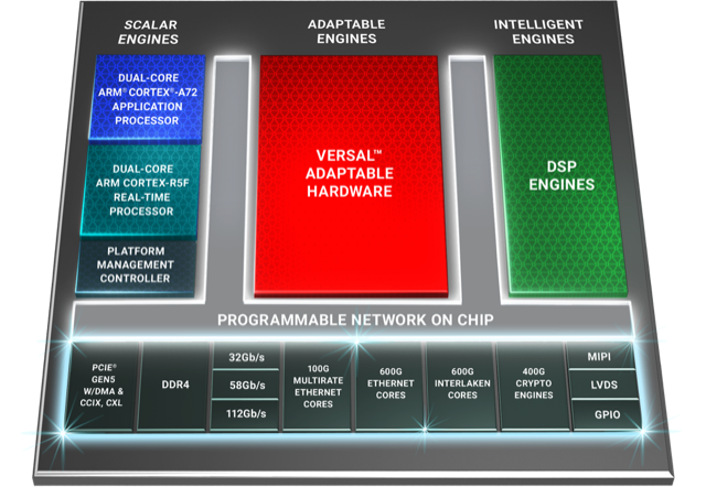
Indeed, Xilinx’s latest programmable logic family, the Versal Premium, is no longer referred to as an FPGA but as an adaptive compute accelerator platform (ACAP).
The Versal Premium series of chips, to be implemented using TSMC’s 7nm CMOS process, was unveiled for the OFC 2020 show. The Premium series will have seven chips with the largest, the VP1802, having 50 billion transistors.
First devices will ship in the second half of 2021.
ACAP series
Xilinx unveiled its adaptive compute acceleration platform in 2018.

Kirk Saban
“It is a complete rearchitecting of our device technology,” says Kirk Saban, vice president product and platform marketing at Xilinx. “It is heterogenous by nature and has multiple types of processing engines.”
“Versal Premium is evolutionary compared with previous FPGAs that have hardened blocks for certain functions,” says Bob Wheeler, principal analyst at The Linley Group. “It is another step along a continuum, not really new.”
Six ACAP families are planned for Versal: three tailored for artificial intelligence (AI) - the AI RF, AI Core and AI Edge - and the others being the Prime, Premium and HBM (high bandwidth memory).
Only Versal AI series will have AI engines: very-long-instructing-word (VLIW) processor cores that can also be used for computational-intensive tasks such as digital signal processing.
Premium is the third Versal family to be unveiled, joining the AI Core and Prime series.
Versal Prime is Xilinx’s broadest series in the portfolio, featuring a range of device sizes and capabilities. The Prime series is suited to such applications as storage acceleration in the data centre; wired networking such as 5G back-, mid- and front-haul, and passive optical networking; and industrial applications such as machine vision.
Networking needs
Versal Premium has been developed with core networking and data centre acceleration applications in mind.
“The top-end SKU handles high-end networking applications such as optical transport and data centre interconnect as well as the most demanding signal-processing applications such as radar systems,” says Wheeler.
Xilinx defines core networking as the infrastructure beyond the radio access network. “All the wireline infrastructure is what we consider to be the core of the network,” says Saban. “Access, metro, and core networks, all together.”
When Xilinx’s designers sat down to consider the networking needs for the coming six years, they anticipated a huge capacity hike in the core network. Device numbers are set to grow tenfold with each device generating ten times more traffic.
“The bandwidth going through the wired network globally needs to grow at 50 per cent on a compound annual basis to keep pace with the number of devices being connected and the data coming through them,” says Saban.
Versal Premium will deliver three times the bandwidth and nearly twice the logic capacity of the 16nm Virtex UltraScale+ VU13P FPGA, the largest device used currently for networking and data centre applications.
“Shifts are happening that the Virtex FPGAs are not going to be able to handle,” says Saban. “The move to 400 gigabit and then 800 gigabit on the mid-term horizon, the Virtex products can’t handle that kind of throughput.”
Versal Premium architecture. Source: Xilinx
Premium architecture
The Premium devices feature ARM-based scalar processors such as the dual-core Cortex-A72 application processor and the dual-core Cortex-R5F real-time processor.
The application processor is used for general-purpose processing and control. The real-time processor is used for applications that require deterministic processing. Such a processor is key for safety-certified applications.
Also included is a platform management controller that oversees the device. A user can configure many of the ACAP settings using a standard tool flow but the controller’s operation is effectively transparent to the user, says Saban.
The Premium features several types of on-chip memory that Saban likens to levels of cache memory used by high-performance processors. ”We have look-up-table RAM, Block RAM and Ultra RAM and we can offload to [external] DDR4 [RAM],” he says. “The memory hierarchy can be configured to match the algorithm you are building.”
The various on-chip functional blocks are linked via a programmable network-on-a-chip. Having the network-on-a-chip frees up programmable logic resources that would otherwise be required to connect the design’s functional blocks.
“Equipment manufacturers need to deliver on this core network growth but they also need to do it securely,” says Saban. “With everything shifting to the cloud, there are huge concerns about data privacy; in many instances, security is just as important as performance for the operators.”
To this aim, the Premium’s on-chip peripherals include 400-gigabit crypto-engines that support the AES-GCM-256 and -128, MACsec, and IPSec encryption standards.
“The crypto blocks are unique and save a lot of look-up tables and power compared with implementing these in programmable logic,” says Linley’s Wheeler.
Other on-chip features include up to 5 terabits of Ethernet throughput supporting rates from 10 to 400 Gigabit Ethernet. The devices have multiple 600-gigabit Ethernet MAC cores and support such protocols as FlexE, Flex-O, Ethernet CPRI (eCPRI), Fibre Channel over Ethernet (FCoE), and OTN.
The Premium family delivers up to 1.8 terabits of Interlaken, from 10-gigabit to 600-gigabit interfaces. Interlaken enables chip-to-chip and chip-to-backplane communications.
There are also 112-gigabit 4-level pulse-amplitude modulation (PAM-4) serialisers/ deserialisers (serdes). The VP1802 will have 28, 32-gigabit serdes and either 140, 58-gigabit or 70, 112-gigabit serdes. The electrical transceivers can drive 10m of copper cable, says Saban.
PCI Express Generation 5.0, enabling direct memory access and cache-coherent interconnect, is also supported on-chip. “We can connect to server CPUs and be an extension of their memory map,” says Saban.
Xilinx claims 22 UltraScale+ FPGAs would be needed to implement all the logic and peripherals of the Versal Premium VP1802.
System design
Wireline vendors want to double the performance with each generation of equipment while keeping platform size and power consumption constant.
Xilinx has a diagram (shown) of a generic telecom line-card design using the Versal Premium. “Vendors have different variants but at a high-level, they all look like this,” says Saban.
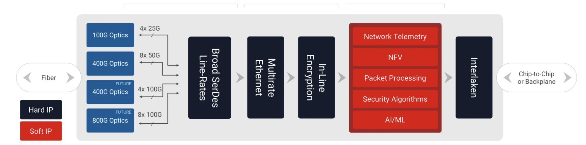
Generic telecom line card using the Versal Premium. Source: Xilinx
Line-card data arrives via optical modules. At present 100-gigabit is mainstream with 400-gigabit coming soon, and eventually 800-gigabit interfaces. The data is fed to the Premium’s hardened logic blocks: the Ethernet and encryption blocks.
The adaptive logic (in red) is what companies use to implement their unique designs such as executing virtualised network functions (NFV) or for packet processing.
“We are seeing the need to infuse artificial intelligence and machine learning into these applications in some capacity,” says Saban. Premium devices have no AI VLIW cores but have sufficient resources for some level of artificial intelligence/ machine learning capability.
Interlaken then sends the data to a host chip or across the backplane to another line card.
Software tools
Xilinx stresses the company is no longer a chip provider but a platform provider. This is reflected in the software tools it provides to accompany its silicon.
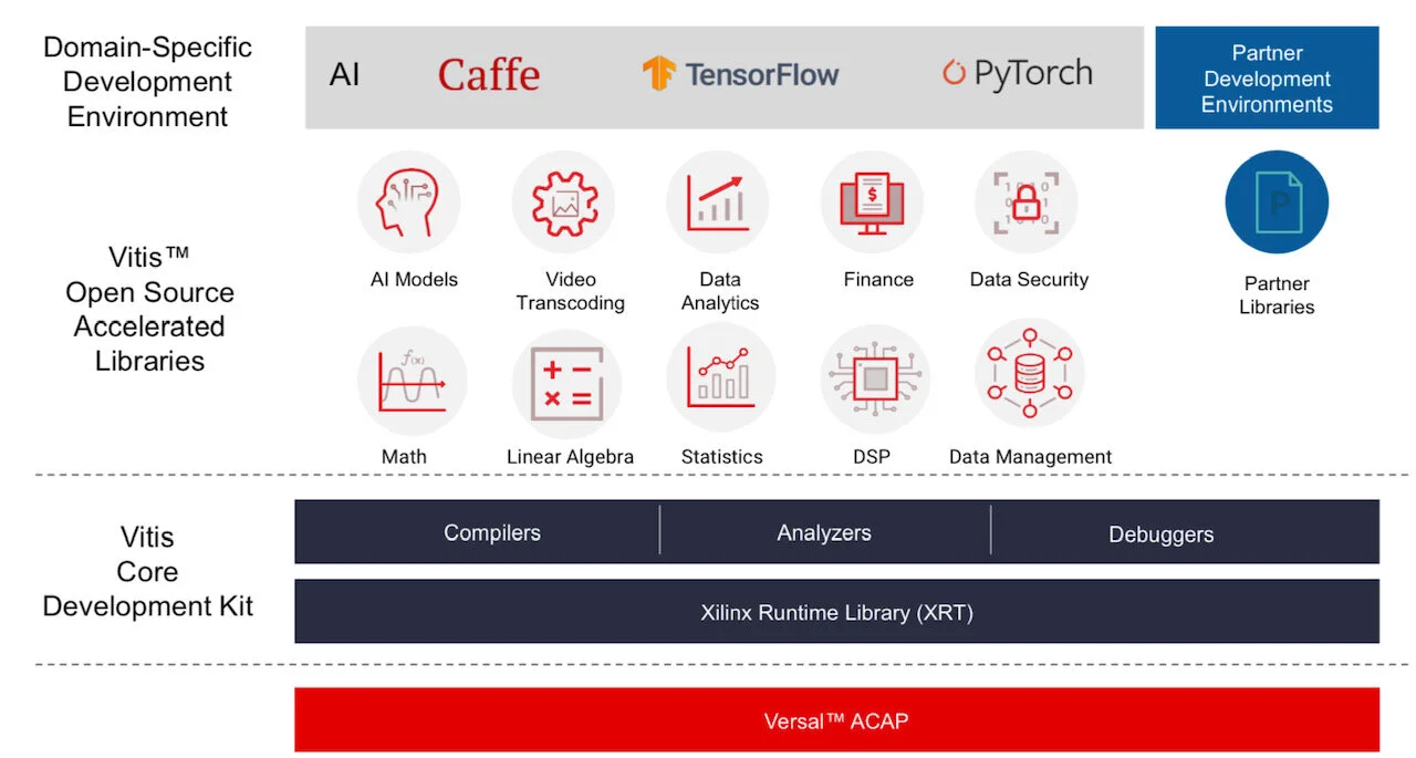
Vitis software tool. Source: Xilinx
Versal ACAPs come with advanced toolkit libraries so engineers can program the chip with no knowledge of the underlying hardware.
Xilinx is continuing to provide its Vivado toolset that supports register-transfer level (RTL), a design abstraction used by hardware engineers for their circuit designs. “The traditional RTL toolchain is not going away and will continue to evolve,” says Saban.
But coders developing data centre applications with no knowledge of RTL or programmable logic can now use Xilinx’s Vitis toolset that was launched in 2019.
“It is critical to enable software developers and data scientists doing machine learning a way to interface to our [ACAP] products,” says Saban.
Vitis supports programming languages such as C, C++ and Python as well as higher-level machine-learning frameworks such as TensorFlow and Caffe.
Xilinx also has a library of functions for tasks such as data analytics and genomics. Such applications can be switched in and out since they are executed using adaptive hardware.
The Premium software tools will be available in the fourth quarter of the year.
Lifespan
A programmable logic family’s lifespan is five or six years; the Virtex UltraScale family was launched in 2015.
“We added a few kickers [to the Virtex family] such as high bandwidth memory and 58-gigabit serdes,” says Saban. “And we will likely do the same with Versal, add some integrated block in a derivative product.”
Xilinx’s chip designers will likely now be already working on an ACAP architecture for 2026 supporting 1.6-terabit speeds and to be implemented using a 5nm CMOS process.
“If we are to deliver twice the bandwidth at half the power, it is not enough to lean on CMOS process technology,” says Saban. “We will need to look at new chip architectures to solve the problems.”
This is challenging. “It gets harder, it gets more expensive and there are less and fewer companies that can afford it,” says Saban.

Silicon Photonics spills over into new markets
The market for silicon photonics is set to grow eightfold by 2025. So claims market research firm, Yole Développement, in its latest report on silicon photonics, a technology that enables optical components to be made on a silicon substrate.
Silicon photonics is also being used in new markets although optical transceivers will still account for the bulk of the revenues in 2025.
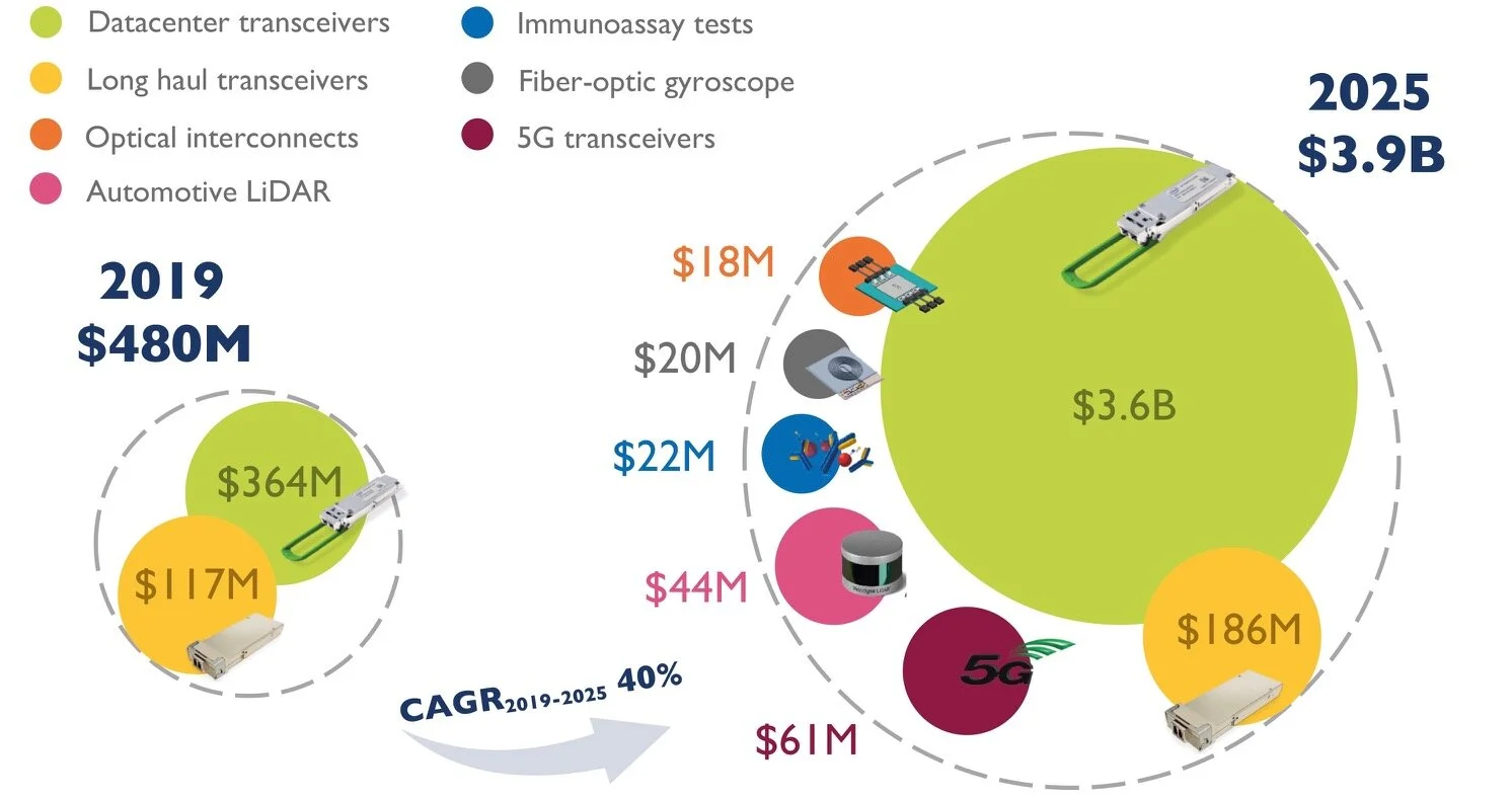
Source: Yole
Market forecast
“We are entering a phase where we are beyond the tipping point [for silicon photonics],” says Eric Mounier, fellow analyst at Yole. “There is no doubt silicon photonics will grow and will be used beyond the data centre.”
Yole sized the 2019 global silicon photonics market at US $480 million, dominated by sales of optical transceivers for the data centre. In 2025 the forecast is for a $3.9 billion market, with data centre transceivers accounting for over 90 per cent of the market.
Eric Mounier
Revenues from new markets such as 5G optical transceivers, automotive, co-packaged optics, fibre-optic gyroscopes, and biochemical sensors will generate $165 million revenues in 2025.
The Yole report also highlights a maturing supply chain, advances in co-packaged optics, and more silicon photonics start-up announcements in the last year.
“It seems the big data centre operators, telecom players and sensor companies are convinced silicon photonics is a key technology for integration, lower cost and smaller components for interconnect and sensing applications,” says Mounier.
Optical transceivers
Data centre optical transceivers account for the bulk of silicon photonics’ market value and unit volumes.
Three-quarters of revenues in 2019 were for data centre transceivers for reaches ranging from several hundred meters to 2km and 10km. This market for silicon photonics is dominated by two players: Intel and Cisco with its Luxtera acquisition.
“For 100-gigabit transceivers, silicon photonics is probably the most used technology compared to legacy optics,” says Mounier.
The remaining 2019 revenues were from long-haul coherent transceiver sales, a market dominated by Acacia that is being acquired by Cisco.
Other companies involved in the transceiver supply chain include Innolight, Juniper Networks, and Alibaba with its work with Elenion Technologies (Elenion was recently acquired by Nokia). HP is working with several firms to develop its silicon photonics supply chain, from device design to final products.
The rollout of 5G is generating a need for 10-gigabit and 25-gigabit transceivers for distances up to 100m, linking remote radio heads and the baseband unit, part of the 5G radio access network.
Yole forecasts a $61 million 5G transceiver market in 2025.
Co-packaged optics
The packaging of optical input-output with a digital chip, known as co-packaged optics, has made notable progress in the last year.
“We are pretty convinced that co-packaged optics is the next big application for silicon photonics,” says Mounier.
Intel has demonstrated its optics packaged with the Tofino 2 Ethernet switch chip it gained with the Barefoot Networks acquisition. “Talking to Intel, I believe in two to three years from now, there will be the first product,” he says.
Other firms pursuing co-packaged optics include Ranovus, Rockley Photonics, Ayar Labs and Sicoya.
The doubling in Ethernet switch-chip capacity every two years is a key driver for co-packaged optics. Switch chips with 25.6-terabit capacity exist and 51.2-terabit switches will be shipping by 2025.
There will also be eight-hundred-gigabit pluggable transceivers in 2025 but Yole says co-packaged optics offers a systems approach to increasing channel counts to keep pace with growing switch capacities.
Foundries and design houses
More than 10 foundries exist worldwide offering silicon photonics services.
“Foundries are interested in silicon photonics because they see a future opportunity for them to fill their fabs,” says Mounier.
Yole cites how GlobalFoundries is working with Ayar Labs, HP with TSMC, Sicoya with IHP Microelectronics, and Rockley Photonics with VTT Memsfab. TSMC also works with Cisco through its Luxtera acquisition.
Swedish MEMS foundry, Silex Microsystems, is developing a portfolio of silicon photonics technology. “They are working with many players developing telecom photonic platforms,” says Mounier.
There are also several design houses offering photonic design services to companies that want to bring products to market. Examples include VLC Photonics, Luceda, Photon Design and Effect Photonics.
Optical design requires know-how that not all firms have, says Mounier. Such silicon photonics design services recall the ASIC design houses that provided a similar service to the electronics industry some two decades ago.
Sensors
Lidar used for autonomous cars and biochemical chips are two emerging sensor markets embracing silicon photonics. Lidar (light detection and ranging) uses light to sense a vehicle’s surroundings.
“Lidar systems are bulky and expensive and a car needs several, at the front, rear and sides,” says Mounier. “Silicon photonics is an emerging platform for the integration of such devices.”
Two Lidar approaches are using silicon photonics: frequency modulation continuous wave (FMCW) Lidar, also known as coherent Lidar, and an optical phased array.
For coherent Lidar, the transmitted frequency of the laser - represented by the local oscillator - and the reflected signal are mixed coherently. This enables phase and amplitude information to be recovered to determine an object’s position and velocity.
SiLC Technologies has developed a FMCW Lidar chip. Working with Varroc Lighting Systems, the two firms have demonstrated Lidar integrated into a car headlamp.
The second approach - an optical phased array - steers the beam of light without using any moving parts.
Lidar is complex and can be implemented using other technologies besides silicon photonics, says Mounier: “Silicon photonics for Lidar has several advantages but it is not clear why the technology will be used in the car or for robotic vehicles.”
In turn, the emerging economic crisis worldwide will likely delay the development of the autonomous car, he says.
Other sensor developments include silicon photonics-based biosensors from Genalyte that use lasers, micro-ring resonators and detectors to produce fast biological test results. The US company has raised over $90 million in three rounds of funding.
French firm Aryballe produces a tiny photonic IC that acts as an electronic nose (digital olfaction). “Using silicon photonics, you can integrate everything on a chip,” says Mounier. “It needs less packaging and assembly and you get a tiny chip at the end.”
COVID-19
Silicon photonics shipments have been delayed in the first half of 2020 due to the COVID-19 pandemic, says Yole. But the market for silicon photonics will still grow this year albeit not at the originally forecasted 10 per cent.
“Everyone is working from home and there is a need for more networking bandwidth,” says Mounier. There will continued demand for transceivers for the data centre and telecom services.
“Market growth will be positive for telecoms, and markets such as defence and medical will not be much impacted,” he says.

CW-WDM MSA charts a parallel path for optics
Artificial intelligence (AI) and machine learning have become an integral part of the businesses of the webscale players.
The mega data centre players apply machine learning to the treasure trove of data collected from users to improve services and target advertising.

Chris Cole
They can also use their data centres to offer cloud-based AI services.
Training neural networks with data sets is so intensive that it is driving new processor and networking requirements.
It is also impacting optics. Optical interfaces will need to become faster to cope with the amount of data, and that means interfaces with more parallel channels.
Anticipating these trends, a group of companies has formed the Continuous-Wave Wavelength Division Multiplexing (CW-WDM) multi-source agreement (MSA).
The CW-WDM MSA will specify lasers sources and the wavelength grids they use. The lasers will operate in the O-band (1260nm-1360nm) used for datacom optics.
The MSA is defining eight, 16 and 32 channels and will build on work done by the ITU-T and the IEEE.
This is good news for the laser manufacturers, says Chris Cole, Chair of CW-WDM MSA (pictured), given they have already shipped millions of lasers for datacom.
“In general, lasers are typically the hardest thing,” he says.
Wavelength count
The majority of datacom pluggable modules deployed today use either one or four optical channels. “When I started in optics 20 years ago it was all about single wavelengths,” says Cole.
Four channels were first used successfully for 40-gigabit interfaces. “That is when we introduced coarse wavelength-division multiplexing (CWDM),” says Cole.
Four wavelengths are the standard approach for 100, 200 and 400-gigabit optical modules. Spreading data across four channels simplifies the design of the electrical and optical interfaces.
“But we are ready to move on because the ability to increase parallel channels - be it parallel fibres or wavelengths - is much greater than the ability to push speed,” says Cole. “If all we do is rely on a four-wavelength paradigm and we keep pushing speed, we will run into a brick wall.”
Integration
Adopting more parallel channels will have two consequences on the optics, says Cole.
One is that photonic integration will become the only practical way to build multi-channel designs. Eight-channel designs are possible using discrete components but it won’t be cost-competitive for designs of 16 or more channels.
“It has to be photonic integration because as you get to eight and later, 16 and 32 wavelengths, it is not supportable in a small size with conventional approaches,” says Cole.
The MSA favours silicon photonics integration but indium phosphide or polymer integration platforms could be used.
The MSA will also cause wavelengths to be packed far more closely than the 20nm used for CWDM. Techniques now exist that enable tighter wavelength spacings without needing dedicated cooling.
One approach is separating the laser from the silicon chip - a switch chip or processor - that generates a lot of heat. Here, light from the source is fed to the optics over a fibre such that temperature control is more straightforward because the laser and chip are separated.
Cole also highlights the athermal silicon photonics of Juniper Networks that controls wavelength drift on the grid without requiring a thermo-electric cooler. Juniper gained the technology with its Aurrion acquisition in 2016.
Specification work
“Using the O-band has a lot of advantages,” says Cole. “That is where all the datacom optics are.”
The optical loss in the O-band may be double that of the C-band but this is not an issue for datacom’s short spans.
The MSA is to define a technology roadmap rather than a specific product, says Cole. First-generation products will use eight wavelengths followed by 16- and then 32-wavelength designs. Sixty-four and even 128 channel counts will be specified once the technology is established.
“Initially we did [specify 64 and 128 channels] but we took it out,” says Cole. “We’ll know a lot more if we are successful over three generations; we’ll figure out what we need to do when we get to that point.”
The MSA is proposing two bands, one 18nm wide (1291nm-1309nm) and the other 36nm wide (1282nm-1318nm). Eight, 16 and 32 wavelengths are assigned across both bands.
“It’s smack in the middle of the CWDM4 grid which is the largest shipping laser grid ever, and it is smack on top of the LWDM4 grid [used by -LR4 modules] which is the next highest grid to ship in volume,” says Cole.
The MSA will also specify continuous-wave laser parameters such as the output power, spectral width, variation in power between the wavelengths, and allowable wavelength shift.
Members
Cole started work on the CW-WDM MSA in collaboration with Ayar Labs while he was still at II-IV. Now at Luminous Computing, Cole, along with MSA editor Matt Sysak of Ayar Labs, and associate editor Dave Lewis of Lumentum, are preparing the first MSA draft and have solicited comments from members as to what to include in the specifications.
The MSA has 11 promoter members: Arista, Ayar Labs, CST Global, imec, Intel, Lumentum, Luminous Computing, MACOM, Quintessent, Sumitomo Electric, and II-VI.
The MSA has created a new observer member status to get input from companies that otherwise would be put off joining an MSA due to the associated legal requirements.
“So we have an observer category that if someone is serious and they want to see a subset of the material the MSA is working on and provide feedback, we welcome that,” says Cole.
The observer members are AMF, Axalume, Broadcom, Coherent Solutions, Furukawa Electric, GlobalFoundries, Keysight Technologies, NeoPhotonics, NVIDIA, Samtec, Scintil Photonics, and Tektronix.
“This MSA is meant to be inclusive, and it is meant to foster innovation and foster as broad an industry contribution as possible,” concludes Cole.
Further information
The CW-WDM MSA has several documents and technical papers on its website. The first document is the CW-WDM MSA grid proposal while the rest are technical papers addressing developments and applications driving the need for high-channel-count optical interfaces.