
Ranovus readies its interfaces for deployment
- Products will be deployed in the first half of 2015
- Ranovus has raised US $24 million in a second funding round
- The start-up is a co-founder of the OpenOptics MSA; Oracle is now also an MSA member.
Ranovus says its interconnect products will be deployed in the first half of 2015. The start-up, which is developing WDM-based interfaces for use in and between data centres, has raised US $24 million in a second stage funding round. The company first raised $11 million in September 2013.
 Saeid Aramideh"There is a lot of excitement around technologies being developed for the data centre," says Saeid Aramideh, a Ranovus co-founder and chief marketing and sales officer. He highlights such technologies as switch ICs, software-defined networking (SDN), and components that deliver cost savings and power-consumption reductions. "Definitely, there is a lot of money available if you have the right team and value proposition," says Aramideh. "Not just in Silicon Valley is there interest, but in Canada and the EU."
The optical start-up's core technology is a quantum dot multi-wavelength laser which it is combining with silicon photonics and electronics to create WDM-based optical engines. With the laser, a single gain block provides several channels while Ranovus is using a ring resonator implemented in silicon photonics for modulation. The company is also designing the electronics that accompanies the optics.
Aramideh says the use of silicon photonics is a key part of the design. "How do you enable cost-effective WDM?" he says."It is not possible without silicon photonics." The right cost points for key components such as the modulator can be achieved using the technology. "It would be ten times the cost if you didn't do it with silicon photonics," he says.
The firm has been working with several large internet content providers to turn its core technology into products. "We have partnered with leading data centre operators to make sure we develop the right products for what these folks are looking for," says Aramideh.
In the last year, the start-up has been developing variants of its laser technology - in terms of line width and output power - for the products it is planning. "A lot goes into getting a laser qualified," says Aramideh. The company has also opened a site in Nuremberg alongside its headquarters in Ottawa and its Silicon Valley office. The latest capital will be used to ready the company's technology for manufacturing and recruit more R&D staff, particularly at its Nuremberg site.
Ranovus is a founding member, along with Mellanox, of the 100 Gigabit OpenOptics multi-source agreement. Oracle, Vertilas and Ghiasi Quantum have since joined the MSA. The 4x25 Gig OpenOptics MSA has a reach of 2km-plus and will be implemented using a QSFP28 optical module. OpenOptics differs from the other mid-reach interfaces - the CWDM4, PSM4 and the CLR4 - in that it uses lasers at 1550nm and is dense wavelength-division multiplexed (DWDM) based.
It is never good that an industry is fragmented
That there are as many as four competing mid-reach optical module developments, is that not a concern? "It is never good that an industry is fragmented," says Aramideh. He also dismisses a concern that the other MSAs have established large optical module manufacturers as members whereas OpenOptics does not.
"We ran a module company [in the past - CoreOptics]; we have delivered module solutions to various OEMs that are running is some of the largest networks deployed today," says Aramideh. "Mellanox [the other MSA co-founder] is also a very capable solution provider."
Ranovus plans to use contract manufacturers in Asia Pacific to make its products, the same contract manufacturers the leading optical module makers use.
 Table 1: The OpenOptics MSA
End markets
"I don't think as a business, anyone can ignore the big players upgrading data centres," says Aramideh. "The likes of Google, Facebook, Amazon, Apple and others that are switching from a three-tier architecture to a leaf and spine need longer-reach connectivity and much higher capacity." The capacity requirements are much beyond 10 Gig and 40 Gig, and even 100 Gig, he says.
Ranovus segments the adopters of interconnect into two: the mass market and the technology adopters. "Mass adoption today is all MSA-based," says Aramideh. "The -LR4 and -SR10, and the same thing is happening at 100 Gig with the QSFP28." The challenge for the optical module companies is who has the lowest cost.
Then there are the industry leaders such as the large internet content providers that want innovative products that address their needs now. "They are less concerned about multi-source standard-based solutions if you can show them you can deliver a product they need at the right cost," says Aramideh.
Ranovus will offer an optical engine as well as the QSFP28 optical module. "The notion of the integration of an optical engine with switch ICs and other piece parts in the data centre are more of an urgent need," he says.
Using WDM technology, the company has a scalable roadmap that includes 8x25 Gig and 16x25 Gig (400 Gig) designs. Also, by adding higher-order modulation, the technology will scale to 1.6 Terabit (16x100 Gig), says Aramideh.
I don't see a roadmap for coherent to become cost-effective to address the smaller distances
Ranovus is also working on interfaces to link data centres.
"These are distances much shorter than metro/ regional networks," says Aramideh, with the bulk of the requirements being for links of 15 to 40km. For such relatively short distances, coherent detection technology has a high-power consumption and is expensive. "I don't see a roadmap for coherent to become cost-effective to address the smaller distances," says Aramideh.
Instead, the company believes that a direct-detection interconnect that supports 15 to 40km and which has a spectral efficiency that can scale to 9.6 Terabit is the right way to go. If that can be achieved, then switching from coherent to direct detection becomes a no-brainer, he says. "For inter-data-centres, we are really offering an alternative to coherent."
The start-up says its technology will be in product deployment with lead customers in the first half of 2015.
ECOC 2014: Industry reflections on the show
Gazettabyte asked several attendees at the recent ECOC show, held in Cannes, to comment on key developments and trends they noted, as well as the issues they will track in the coming year.
Daryl Inniss, practice leader, components at market research firm, Ovum
 It took a while to unwrap what happened at ECOC 2014. There was no one defining event or moment that was the highlight of the conference.
The location was certainly beautiful and the weather lovely. Yet I felt the participants were engaged with critical technical and business issues, given how competitive the market has become.
Kaiam’s raising US $35 million, Ranovus raising $24 million, InnoLight Technology raising $38 million and being funded by Google Capital, and JDSU and Emcore each splitting into two companies, all are examples of the shifting industry structure.
On the technology and product development front, advances in 100 Gig metro coherent solutions were reported although products are coming to market later than first estimated. The client-side 100 Gig is transitioning to CFP2. Datacom participants agree that QSFP28 is the module but what goes inside will include both parallel single mode solutions and wavelength multiplexed ones.
Finisar’s 50 Gig transmission demonstration that used silicon photonics as the material choice surprised the market. Compared to last year, there were few multi-mode announcements. ECOC 2014 had little excitement and no one defining show event but there were many announcements showing the market’s direction.
There is one observation from the show, which while not particularly exciting or sexy, is important, and it seems to have gone unnoticed in my opinion. Source Photonics demonstrated the 100GBASE-LR4, the 10km 100 Gigabit Ethernet standard, in the QSFP28 form factor. This is not new as Source Photonics also demonstrated this module at OFC. What’s interesting is that no one else has duplicated this result.
There will be demand for a denser -LR4 solution that’s backward compatible with the CFP, CFP2, and CFP4 form factors. It is unlikely that the PSM4, CWDM4, or CLR4 will go 10km and they are not optically compatible with the -LR4. The market is on track to use the QSFP28 for all 100 Gig distances so it needs the supporting optics. The Source Photonics demonstration shows a path for 10km. We expect to see other solutions for longer distances over time.
One surprise at the show was Finisar's and STMicroelectronics's demonstration of 50 Gig non-return-to-zero transmission over 2.2km on standard single mode fiber. The transceiver was in the CFP4 form factor and uses heterogeneous silicon technologies inside. The results were presented in a post-deadline paper (PD.2.4). The work is exciting because it demonstrates a directly modulated laser operating above 28 Gig, the current state-of-the-art.
The use of silicon photonics is surprising because Finisar has been forced to defend its legacy technology against the threat of transceivers based on silicon photonics. These results point to one path forward for next-generation 100 Gig and 400 Gig solutions.
In the coming year, I’m looking for the dominant metro 100G solution to emerge. When will the CFP2 analogue coherent optical module become generally available? Multiple suppliers with this module will help unleash the 100 Gig line-side transmission market, drive revenue growth and the development for the next-generation solution.
Slow product development gives competing approaches like the digital CFP a chance to become the dominant solution. At present, there is one digital CFP vendor with a generally available product, Acacia Communications, with a second, Fujitsu Optical Components, having announced general availability in the first half of 2015.
Neal Neslusan, vice president of sales and marketing at fabless chip company, MultiPhy.
It was impressive to see Oclaro's analogue CFP2 for coherent applications on the show floor, albeit only in loopback mode. Equally impressive was seeing ClariPhy's DSP on the evaluation board behind the CFP2.
 I saw a few of the motherboard-based optics solutions at the show. They looked very interesting and in questioning various folks in the business I learned that for certain data centre applications these optics are considered acceptable. Indeed, they represent an ability to extract much higher bandwidth from a given motherboard as compared to edge-of-the-board based optics, but they are not pluggable.
Traditionally, pluggable optics has been the mainstay of the datacom and enterprise segments and these motherboard-based optics have been relegated to supercomputing. This is just another example, in my opinion, of how the data centre market is becoming distinct from the datacom market.
Where there any surprises at the show? I was surprised and alarmed at the cost of the Martini drinks at the hotel across the street from the show, and they weren't even that good!
Regarding developments in the coming year, the 8x50 Gig versus 4x100 Gig fight in the IEEE is clearly a struggle I will follow. I think it will have a great impact on product development in our industry. If 8x50 Gig wins, it may be one of the few times in the history of our industry that a less advanced solution is chosen over a more advanced and future-proofed one.
The physical size of the next-generation Terabit Ethernet switch chips will have a much larger impact on the optics they connect to in the coming years, compared to the past. This work combined with the motherboard-based optics may create a significant change in the solutions brought to bear for high-performance communications.
John Lively, principal analyst at market research firm, LightCounting.
 There were several developments that I noted at the show. ECOC helped cement the view that 100 Gig coherent is mainstream for metro networks. Also more and more system vendors are incorporating Raman/ remote optically pumped amplifier (ROPA) into their toolkit. ROPA is a Raman-based amplifier where the pump is located at one end of the link, not in some intermediate node. Another trend evident at ECOC is how the network boundary between terrestrial and submarine is blurring.
As for developments to watch, I intend to follow mobile fronthaul/ backhaul, higher speed transceiver developments, of course, and how the mega-data-centre operators are disrupting networks, equipment, and components.
For the ECOC reflections, final part, click here
Finisar adds silicon photonics to its technology toolkit
- Finisar revealed its in-house silicon photonics design capability at ECOC
- The company also showed its latest ROADM technologies: a dual wavelength-selective switch and a high-resolution optical channel monitor.
- Also shown was an optical amplifier that spans 400km fibre links

These two complementary technologies [VCSELs and silicon photonics] work well together as we think about the next-generation Ethernet applications.
Rafik Ward
Finisar demonstrated at ECOC its first optical design implemented using silicon photonics. The photonic integrated circuit (PIC) uses a silicon photonics modulator and receiver and was shown operating at 50 Gigabit-per-second.
The light source used with the PIC was a continuous wave distributed feedback (DFB) laser. One Finisar ECOC demonstration showed the eye diagram of the 50 Gig transmitter using non-return-to-zero (NRZ) signalling. Separately, a 40 Gig link using this technology was shown operating error-free over 12km of single mode fibre.
"Finisar, and its fab partner STMicroelectronics, surprised the market with the 50 Gig silicon photonics demonstration,” says Daryl Inniss, practice leader of components at Ovum.
"This, to our knowledge, was the first public demonstration of silicon photonics running at such a high speed," says Rafik Ward, vice president of marketing at Finisar. However, the demonstrations were solely to show the technology's potential. "We are not announcing any new products," he says.
Potential applications for the PIC include the future 50 Gig IEEE Ethernet standard, as well as a possible 40 Gig serial Ethernet standard. "Also next-generation 400 Gig Ethernet and 100 Gig Ethernet using 50 Gig lanes," says Ward. "All these things are being discussed within the IEEE."
Jerry Rawls, co-founder and chairman of Finisar, said in an interview a year ago that the company had not developed any silicon photonics-based products as the technology had not shown any compelling advantage compared to its existing optical technologies.
Now Finisar has decided to reveal its in-house design capability as the technology is at a suitable stage of development to show to the industry. It is also timely, says Ward, given the many topics and applications being discussed in the standards work.
The company sees silicon photonics as part of its technology toolkit available to its engineers as they tackle next-generation module designs.
Finisar unveiled a vertical-cavity surface-emitting laser (VCSEL) operating at 40 Gig at the OFC show held in March. The 40 Gig VCSEL demonstration also used NRZ signalling. IBM has also published a technical paper that used Finisar's VCSEL technology operating at 50 Gbps.
"What we are trying to do is come up with solutions where we can enable a common architecture between the short wave and the long wave optical modules," says Ward. "These two complementary technologies [VCSELs and silicon photonics] work well together as we think about the next-generation Ethernet applications."
Cisco Systems, also a silicon photonics proponent, was quoted in the accompanying Finisar ECOC press release as being 'excited' to see Finisar advancing the development of silicon photonics technology. "Cisco is our biggest customer," says Ward. "We see this as a significant endorsement from a very large user of optical modules." Cisco acquired silicon photonics start-up Lightwire for $271 million in March 2012.
ROADM technologies
Finisar also demonstrated two products for reconfigurable optical add/ drop multiplexers (ROADM): a dual configuration wavelength-selective switch (WSS) and an optical channel monitor (OCM).
The dual-configuration WSS is suited to route-and-select ROADM architectures.
Two architectures are used for ROADMs: broadcast-and-select and route-and-select. With broadcast-and-select, incoming channels are routed in the various directions using a passive splitter that in effect makes copies of the incoming signal. To route signals in the outgoing direction, a 1xN WSS is used. However, due to the optical losses of the splitters, such an architecture is used for low node-degree applications. For higher-degree nodes, the optical loss becomes a barrier, such that a WSS is also used for the incoming signals, resulting in the route-and-select architecture. A dual-configuration WSS thus benefits a route-and-select ROADM design.
Finisar's WSS module is sufficiently slim that it occupies a single-chassis slot, unlike existing designs that require two. "It enables system designers to free up slots for other applications such as transponder line cards inside their chassis," says Ward.
The dual WSS modules support flexible grid and come in 2x1x20, 2x1x9 and 2x8x12 configurations. "There are some architectures being discussed for add/ drop that would utilise the WSS in that [2x8x12] configuration," says Ward.
The ECOC demonstrations included different traffic patterns passing through the WSS, as well as attenuation control and the management of super-channels.
Finisar also showed an accompanying high-resolution OCM that also occupies a single-chassis slot. The OCM can resolve the spectral power of channels as narrow as 6.25GHz. The OCM, a single-channel device, can scan a fibre's C-band in 200ms.
A rule of thumb is that an OCM is used for each WSS. A customer often monitors channels on a single fibre, says Ward, and must pick which fibres to monitor. The OCM is typically connected to each fibre or to an optical switch to scan multiple fibres.
"People are looking to use the spectrum in a fibre in a much more optimised way," says Ward. The advent of flexible grid and super-channels requires a much tighter packing of channels. "So, being able to see and identify all of the key elements of these channels and manage them is going to become more and more difficult," he says, with the issue growing in importance as operators move to line speeds greater than 100 Gig.
Finisar also used the ECOC show to demonstrate repeater-less transmission using an amplifier that can span 400km of fibre. Such an amplifier is used in harsh environments where it is difficult to build amplifier huts. The amplifier can also be used for certain submarine applications known as 'festooning' where the cable follows a coastline and returns to land each time amplification is required. Using such a long-span amplifier reduces the overall hops back to the coast.
OFC 2014 industry reflections - Part 2

The high cost of 100 Gigabit Ethernet client modules has been a major disappointment to me as it has slowed adoption
Joe Berthold, Ciena
Joe Berthold, vice president of network architecture at Ciena.
OFC 2014 was another great event, with interesting programmes, demonstrations and papers presented. A few topics that really grabbed my interest were discussions around silicon photonics, software-defined networking (SDN) and 400 Gigabit Ethernet (GbE).
The intense interest we saw at last year’s OFC around silicon photonics grew this year with lots of good papers and standing-room-only sessions. I look forward to future product announcements that deliver on the potential of this technology to significantly reduce cost of interconnecting systems over modest distances. The high cost of 100GbE client modules has been a major disappointment to me as it has slowed adoption.
Another area of interest at this year’s show was the great deal of experimental work around SDN, some more practical than others.
I particularly liked the reviews of the latest work under the DARPA-sponsored CORONET programme, whose Phase 3 focused on SDN control of multi-layer, multi-vendor, multi-data centre cloud networking across wide area networks.
In particular, there were talks from three companies I noted: Anne Von Lehman of Applied Communication Sciences, the prime contractor, provided a good program overview; Bob Doverspike of AT&T described a very extensive testbed using equipment of the type currently deployed in AT&T’s network, as well as two different processing and storage virtualisation platforms; and Doug Freimuth of IBM described its contributions to CORONET including an OpenStack virtualisation environment, as well as other IBM distributed cloud networking research.
All the action on rates above 100 Gig lies with the selection of client signals. 400 Gig seems to have the major mindshare but there are still calls for flexible rate clients and Terabit clients.
One thing I enjoyed about these talks was that they described an approach to SDN for distributed data centre networking that is pragmatic and could be realised soon.
I also really liked a workshop held on the Sunday on the question whether SDN will kill GMPLS. While there was broad consensus that GMPLS has failed in delivering on its original turn-of-the-century vision of IP routers control of multi-layer, multi-domain networks, most speakers recognised the value distributed control planes have in simplifying and speeding the control of single layer, single domain networks.
What I took away was that single layer distributed control planes are here to stay as important network control functions, but instead will work under the direction of an SDN network controller.
As we all know, 400 Gigabit dense wavelength division multiplexing (DWDM) is here from the technology perspective, but awaiting standardisation of the 400 Gig Ethernet signal from the IEEE, and follow-on work by the ITU-T on signal mapping to OTN. In fact, from the perspective of DWDM transmission systems, 1 Terabit-per-second systems can be had for the asking.
All the action on rates above 100 Gig lies with the selection of client signals. 400 Gig seems to have the major mindshare but there are still calls for flexible rate clients and Terabit clients.
One area that received a lot of attention, with many differing points of view, was the question of the 400GbE client. As the 400GbE project begins soon in the IEEE, it is time to take a lesson from the history of the 100 Gig client modules and do better.
Let us all agree that we don’t need 400 Gig clients until they can do better in cost, face plate density, and power dissipation than the best 100 Gig modules that will exist then.
The first 100 Gig DWDM transceivers were introduced in 2009. It is now 2014 and 100 Gig is the transmission rate of choice for virtually all high capacity DWDM network applications, with a strong economic value proposition versus 10 Gig. Yet the industry has not yet managed to achieve cost/bit parity between 100 Gig and 10 Gig clients - far from it!
Last year's OFC, we saw many show floor demonstrations of CFP2 modules. They promise lower costs, but evidence of their presence in shipping products is still lacking. At the exhibit this year we saw 100 Gig QSFP28 modules. While progress is slow, the cost of the 100 Gig client module continues to result in many operators favouring 10 Gig handoffs to their 100 Gig optical networking systems.
Let us all agree that we don’t need 400 Gig clients until they can do better in cost, face plate density, and power dissipation than the best 100 Gig modules that will exist then. At this juncture the 100 Gig benchmark we should be comparing 400 Gig to is a QSFP28 package.
Lastly, last year we heard about the launch of an OIF project to create a pluggable analogue coherent optical module. There were several talks that referenced this project, and discussed its implications for shrinking size and supporting higher transceiver card density.
Broad adoption of this component will help drive down costs of coherent transceivers, so I look forward to its hearing about its progress at OFC 2015.
Daryl Inniss, vice president and practice leader, Ovum.
There was no shortage of client-side announcements at OFC and I’ve spent time since the conference trying to organise them and understand what it all means.
I’m tempted to say that the market is once again developing too many options and not quickly agreeing on a common solution. But I’m reminded that this market works collaboratively and the client-side uncertainty we’re seeing today is a reflection of a lack of market clarity.
Let me describe three forces affecting suppliers:
The IEEE 100GBASE-xxx standards represent the best collective information that suppliers have. Not surprisingly, most vendors brought solutions to OFC supporting these standards. Vendors sharpened their products and focused on delivering solutions with smaller form factors and lower power consumption. Advances in optical components (lasers, TOSAs and ROSAs), integrated circuits (CDRs, TIAs, drivers), transceivers, active optical cables, and optical engines were all presented. A promising and robust supply base is emerging that should serve the market well.
A second driver is that hyperscale service providers want a cost-effective solution today that supports 500m to 2km. This is non-standard and suppliers have not agreed on the best approach. This is where the market becomes fragmented. The same vendors supporting the IEEE standard are also pushing non-standard solutions. There are at least four different approaches to support the hyperscale request:
- Parallel single mode (PSM4) where an MSA was established in January 2014
- Coarse wavelength division multiplexing—using uncooled directly modulated lasers and single mode fibre
- Dense wavelength division multiplexing—this one just emerged on the scene at OFC with Ranovus and Mellanox introducing the OpenOptics MSA
- Complex modulation—PAM-8 for example and carrier multi-tone.
Admittedly, the presence of this demand disrupts the traditional process. But I believe the suppliers’ behavior reflects their unhappiness with the standardisation solution.
The good news is these approaches are using established form factors like the QSFP. And silicon photonic products are starting to emerge. Suppliers will continue to innovate.
Ambiguity will persist but we believe that clarity will ultimately prevail.
The third issue lurking in the background is knowledge that 400 Gig and one Terabit will soon be needed. The best-case scenario is to use 100 Gig as a platform to support the next generation. Some argue for complex modulation as you reduce the number of optical components thereby lowering cost. That’s good but part of the price is higher power consumption, an issue that is to be determined.
Part of today’s uncertainty is whether the standard solution is suitable to support the market to the next generation. Sixteen channels at 25 Gig is doable but feels more like a stopgap measure than a long-term solution.
These forces leave suppliers innovating in search of the best path forward. The approaches and solutions differ for each vendor. Timing is an issue too with hyperscale looking for solutions today while the mass market may be years away.
We believe that servers with 25 Gig and/ or 40 Gig ports will be one of the catalysts to drive the mass market and this will not start until about 2016. Meanwhile, each vendor and the market will battle for the apparent best solution to meet the varying demands. Ambiguity will persist but we believe that clarity will ultimately prevail.
Acacia uses silicon photonics for its 100G coherent CFP
Acacia Communications has revealed the innards of its 100 Gig coherent pluggable module for metro networks. The AC-100 CFP combines a low-power DSP-ASIC with a silicon-photonics-based optics chip. The CFP's reach is 80km to 1,200km, and its power consumption is 24-26W, well within the pluggable's maximum power profile of 32W.
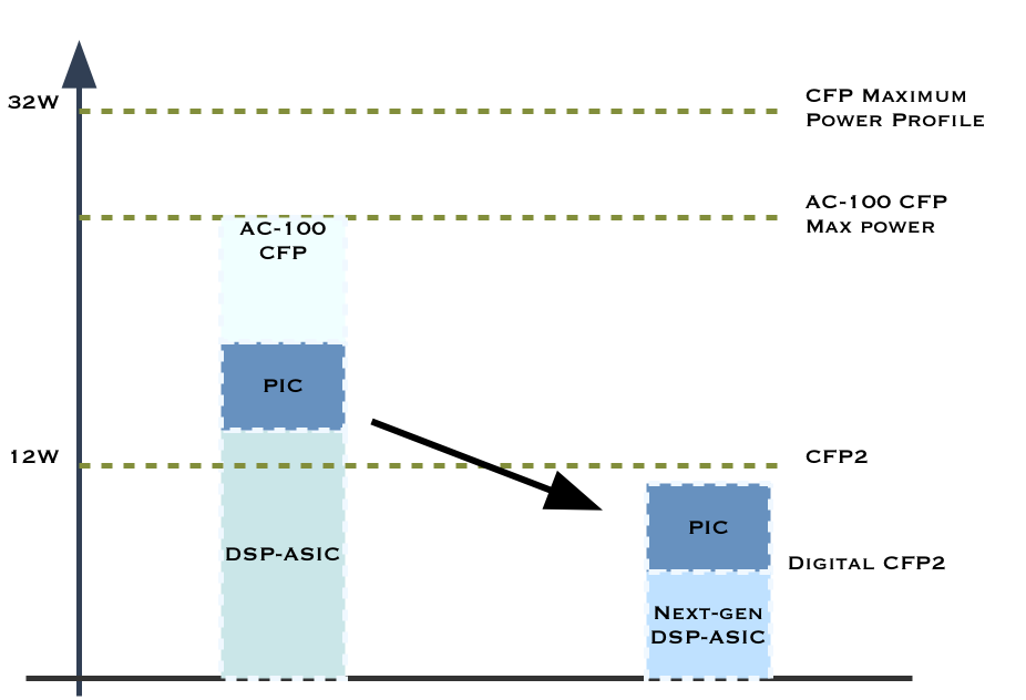 The power consumption of the AC-100 CFP, and its main components, and the target power consumptions of the components needed for a digital CFP2. Source: Gazettabyte
The start-up says it is shipping samples of the AC-100 CFP and already has 15 customers. "That includes some of the bigger [systems] players that have their own internal DSP," says Raj Shanmugaraj, CEO of Acacia. "The coherent CFP is not their focus; they are going after long-haul."
The start-up is shipping samples of the AC-100 CFP and already has 15 customers
Acacia chose to develop it own DSP chips as it sees the technology as core for coherent-based optical transmission. "That is where we see the big market," says Shanmugaraj. "We have a 100 Gig [MSA] that has been shipping, and a 200-400 Gig product that is in development."
DSP-ASIC and silicon photonics
The DSP-ASIC for the AC-100 CFP is Acacia's second chip design. Its first, a DSP-ASIC for its long-haul 5x7-inch OIF MSA transponder, is implemented using a 40nm CMOS process. The latest metro DSP-ASIC uses 28nm CMOS.
The DSP-ASIC includes analogue-to-digital (A/D) and digital-to-analogue (D/A) converters and a serialiser/ deserialiser (Serdes). Also on-chip is the digital signal processor (DSP) that implements soft-decision, forward error correction (SD-FEC) and compensation algorithms for chromatic and polarisation-mode dispersion.
Other DSP-ASIC features include spectral shaping for flexible grid transmission. "The signal processing on the transmit side fits in the one ASIC," says Benny Mikkelsen, CTO at Acacia. Also on-chip are a 100 Gig OTN (Optical Transport Network) framer and a microprocessor to manage the DSP-ASIC and the overall CFP.
The DSP-ASIC consumes 12-14W: the A/D, D/A converters and Serdes consume 5W, while the DSP consumes 7W for an 80km link - the 100 Gig equivalent of the -ZR spec - and 9W for 1,200km transmission due to the more powerful SD-FEC needed.
Mikkelsen says achieving a low-power ASIC requires several approaches. The SD-FEC is designed to be extremely low power, he says, as is the dispersion compensation: "Not just the algorithms but how we code the algorithms." Also, how the ASIC's circuitry is laid out impacts power consumption.
Acacia's engineers have also developed a silicon-photonics chip that combines the coherent transmitter and receiver optics. "The PIC [photonic integrated circuit] is the first silicon-photonics chip targeted at metro/ metro-regional," says Shanmugaraj. "It is an IC that has all the components except the laser, and is co-packaged in a gold box with the drivers and trans-impedance amplifiers."
Acacia's PIC is monolithic; all the functional blocks are implemented in silicon rather than combined silicon and III-V materials, a technique known as heterogeneous integration.
Using silicon photonics rather than indium phosphide has advantages, says Shanmugaraj. Silicon photonics benefits from mature CMOS processes developed for the semiconductor industry: "With the large silicon wafers, you can have thousands of these silicon PICs on them," he says.
Acacia tests the PICs directly on the wafer. This avoids having to dice the wafer and package each die before testing. "We also don't need thermal control [of the chip] or hermetic packaging," says Shanmugaraj. With indium phosphide, the modulators do require thermal cooling, adding to the design complexity and the power consumption. The PIC is 10mm long and consumes less than 5W.

The AC-100 CFP is expected to cost less than half the 5x7-inch 100 Gig coherent MSA which sells for $20,000. "One of the biggest pain points in metro is cost, if you ask most of the service providers," says Shanmugaraj. At below $10,000, the coherent CFP will be cost-competitive with the 100 Gig direct-detection CFP that uses 4x25 Gig wavelengths. However, the 100 Gig direct-detection CFP continues to come down in price as more products come to market.
Roadmap
Acacia will continue to address long-haul and metro, each requiring its own ASIC. "We don't believe that you can have one ASIC that serves both submarine and the metro," says Mikkelsen. In turn, silicon photonics will be used for pluggables while discrete optics will be used for the more demanding submarine.
The company says it is developing a multi-core ASIC to support super-channels and 16-QAM modulation for 200 Gig and 400 Gig transmission. The company says it will provide more details of its flexible, adaptive-rate ASIC at ECOC, to be held in September this year.
The company's product roadmap also features a co-packaged DSP-ASIC and PIC that will fit within a CFP2. Achieving such a pluggable, dubbed a digital CFP2, require a further halving of the DSP-ASIC's power consumption. This, says Acacia, is achievable using the next CMOS process node after 28nm.
The advantages of a digital CFP2 compared to a CFP2 with optics only, with the DSP-ASIC on the line card, include using the DSP-ASIC only when it is needed. When a fault occurs, the relevant pluggable can be replaced rather than having to remove the complete line card. Lastly, new functionality in the DSP-ASIC can be introduced by plugging in the new CFP2 pluggable compared with having to redesign the line card.
See also:
Transmode adopts 100 Gigabit coherent CFPs, click here
ClariPhy samples a 200 Gigabit coherent DSP-ASIC, click here
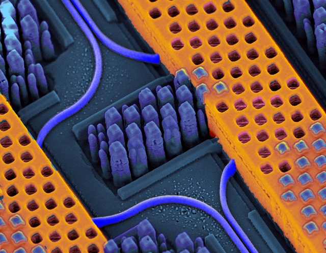
X-Celeprint brings printing technology to silicon photonics
 X-Celeprint's micro transfer printing technology. Source: X-Celeprint
- X-Celeprint has a printing process that places individual 'chiplets' of III-V material onto silicon
- The micro transfer printing technique can be used to make silicon photonics circuits
- X-Celeprint will work with silicon photonics companies interested in licensing its technology
A key challenge facing silicon photonics players is creating a light source. Silicon does not lase so a III-V material is needed to form the laser.
One approach is to attach a tiny module holding the laser to the silicon photonics design. This is what the likes of Cisco Systems, Luxtera, Mellanox Technologies and IBM are doing: adding an external laser to the otherwise monolithic silicon photonics circuit.
An alternative technique is to bond the III-V material to the silicon and using photolithography and etching to construct the silicon photonics device. The attraction of III-V bonding is that the technique can be used to also make the modulators and photo-detectors. Known as heterogeneous integration, this approach is being used by companies such as Aurrion, Intel and Skorpios Technologies.
"Bonding is an elegant solution," says Roel Baets, a professor at the Photonics Research Group at Ghent University. "You can make the light source at the wafer scale and have a single chip solution that looks like a monolithic chip, including the light source."
Think of printing as pick-and-place in a massively parallel fashion. Instead of ink, we are picking up and printing arrays of high-performance semiconductors.
Bonding III-V material to silicon is itself non-trivial. First, silicon wafers are either 200mm or 300mm (8 or 12 inch) while III-V indium phosphide wafers are typically 50mm (2 inch). Indium phosphide wafers are also expensive, simply etching away the majority of the wafer to leave small islands of wanted material is hugely wasteful.
"There is only going to be a laser here or there, with a fill factor - an area coverage - of some one percent," says Baets. "You are throwing away a lot of III-V."
Equally, cutting up the III-V wafer into small slivers for bonding is complicated as it requires precision placement; a process difficult to automate to achieve high-yield circuits. This is the challenge the heterogeneous integration companies have set themselves.
It is a market opportunity identified by start-up X-Celeprint. It has a process that places individual 'chiplets' of III-V material onto silicon by the thousands.
X-Celeprint uses a micro transfer printing to place the chiplets onto silicon. "Think of printing as pick-and-place in a massively parallel fashion," says Kyle Benkendorfer, CEO of X-Celeprint. "Instead of ink, we are picking up and printing arrays of high-performance semiconductors."
Micro transfer printing is already used commercially to make high concentration solar cells, and it is being evaluated to place thin lasers on read/ write heads in disc drives. "We can print live devices or a slab of material on any substrate as long as it is flat," says Benkendorfer.
One benefit of the technique is that the thin III-V material is removed from the indium phosphide wafer but the underlying substrate is retained and can be recycled. For wafer-to-wafer bonding, in contrast, the substrate must be ground back. "This is several hundred microns of [substrate] material," says Benkendorfer. "With our process you can reprocess the wafer and regrow it, saving some $3,000."
The printing process also lends itself to automation. "We can very efficiently place active die of highly expensive compound material at the point of use, where it can then be converted into a device," he says.
X-Celeprint wants to work with silicon photonics companies interested in licensing its printing technology. Developing the process with a particular silicon photonics vendor takes time. Each application requires tailoring and it can take up to two years to make, test and scale up production, says the start-up.
"We recognise that silicon photonics as a large market is out there, no question," says Benkendorfer. "But the development time to get any significant market is going to be a while."
Intel on silicon photonics and its role in the data centre

In the next couple of years, you will see a massive adoption of silicon photonics into the data centers and into high-performance computing
Mario Paniccia, Intel
Bringing new technology to market is at least a decade-long undertaking. So says Mario Paniccia, Intel Fellow and general manager of the company's silicon photonics operation. “The first transistor, the first chip; it has been 10 or 15 years from the first idea or research result to a commercial product,” he says. “Silicon photonics is just another example.”
Paniccia should know. He has been at Intel for nearly 20 years and started the company’s investigation of silicon photonics. Paniccia has overseen each of Intel’s various silicon photonics' building-block developments, beginning with a 1 Gigabit silicon modulator in 2004 through to its high gain-bandwidth avalanche photo-detector detailed in 2008.
Now Intel has unveiled its first 100 Gigabit silicon photonic product used as part of its Rack Scale Architecture (RSA) that implements a disaggregated system design that separates storage, computing and networking. The 100 Gigabit modules are used along with Terabit connectors and Corning's ClearCurve multi-mode fibre.
"Silicon photonics is the path to low-cost, high-volume optical connectivity in and around the server platform and in the data centre,” says Paniccia. “We can see it now coming.”
We are operating with a mindset of CMOS compatibility and we are putting our process and our photonics into fabs that also run high volume CMOS manufacturing
A key advantage of silicon photonics is its ability to benefit from high-volume manufacturing developed for the chip industry. But high-volume manufacturing raises its own challenges, such as determining where silicon photonics has value and picking the right applications.
Another merit, which at first does not sound like one, is that silicon photonics is 'good enough'. “But that 'good enough' is getting better and getting very close to performance levels of most of the modulation and detection devices people have shown in excess of 40 Gig," says Paniccia.
Such silicon-photonic building blocks can be integrated to deliver aggregate bandwidths of 100 Gig, 400 Gig, even a Terabit-per-second. “As demands increase in the data centre, cloud and high-performance computing, the ability to integrate photonics devices with CPUs or ASICs to deliver solutions at an architecture level, that is the really exciting part," says Paniccia.
At the end of the day, it is about building a technology that is cost effective for the application
Manufacturing process
Intel has not said what process it uses for its silicon photonic devices, although it does say it uses more than one. IBM uses 90nm lithography and STMicroelectronics has chosen 65nm for their silicon photonic designs.
Intel makes its photonics and associated drive electronics on separated devices due to the economics. Not using a leading manufacturing process for the photonics is cheaper since it avoids having to use expensive die and associated masks. “At the end of the day, it is about building a technology that is cost effective for the application," says Paniccia.
Intel uses a 22nm CMOS process and is moving to 14nm for its CPUs. For light, the feature sizes in silicon are far broader. “However, better lithography gets you better resolution, gets you better sidewalls roughness and better accuracy,” says Paniccia. “[A] 90nm [lithography] is plenty for most of the process nodes.”
Intel says it uses more advanced lithography for the early manufacturing steps of its silicon photonics devices, while the ’backend’ processing for its hybrid (silicon/ indium phosphide) laser involved broad metal lines and etch steps for which 130nm lithography is used.
The silicon photonics process is designed to be CMOS compatible so that the photonics can be made alongside Intel's volume chips. “That is critical,” says Paniccia. “We are operating with a mindset of CMOS compatibility and we are putting our process and our photonics into fabs that also run high volume CMOS manufacturing." The goal is to ensure that as production ramps, Intel can move its technology across plants.
The company has no plans to offer silicon photonics manufacturing as a foundry business.
Data centre trends
Intel is focussing its silicon photonics on the data centre. “We announced the RSA, a rack connected with switching, with silicon photonics and the new MXC cable,” says Paniccia. “Bringing optics up and down the racks and across racks, not only are the volumes quite big but the price points are aggressive.”
The company is using multi-mode fibre for its silicon photonics solution despite growing interest in single-mode fibre to meet the longer reach requirements emerging in the data centre.
Intel chose multi-mode as it results in a more economic solution in terms of packaging, assembly and cabling. "If you look at a single-mode fibre solution - coupling the fibre, packaging and assembling - it is very expensive," he says. That is because single-mode fibre requires precise fibre alignment at the module and at the connector, he says: "Even if the photonics were free, packaging, testing and assembly accounts for 40-60 percent of cost."
Silicon photonics is inherently single-mode and making it work with multi-mode fibre is a challenge. “At the transmitter side it is somewhat easy, a small hose - the transmitter - going into a big hose, a 50-micron [multi-mode] fibre, so the alignment is easy,“ says Paniccia. “At the receiver side, I now have a 50-micron multi-mode fibre and couple it down into a silicon photonic chip; that is the hard part.”
Corning's ClearCurve multi-mode fibre and the MXC connector working with Intel's 100 Gigabit modules achieve a 300m reach, while 820m has been demonstrated. “At the end of the day, the customer will decide how do we drive a new architecture into the next-generation of data centre,” says Paniccia.
Optics edge closer
Optics will edge up to chips as silicon photonics evolves. With electrical signals moving from 10 Gigabit to 25 Gigabit, it becomes harder to send the signals off chip. Embedding the optics onto the board, as Intel has done with its RSA, means that the electrical signal paths are only a couple of inches long. The signals are then carried optically via the MXC connector that supports up to 64 fibres. "Optical modules are limited in space and power," says Paniccia. "You have got to move to an embedded solution which enables greater faceplate density."
The next development after embedded modules will be to co-package the optics with the ASIC or CPU. "That is the RSA," says Paniccia. "That is the evolution that will have to happen when data rates run from 25 Gig to 32 Gig and 40 Gig line rates."
Moreover, once optics are co-packaged with an ASIC or a CPU, systems will be designed differently and optimised further, says Paniccia. "We have an Intel roadmap that takes it from a core technology for networking all the way to how we attach this stuff to CPUs," he says. "That is the end game."
Intel views silicon photonics not as a link technology but a connectivity approach for an architecture and platforms that will allow customers to evolve as their cloud computing and storage requirements grow.
"In the next couple of years, you will see a massive adoption of silicon photonics into the data centers and into high-performance computing, where the cost of I/O [input/output] has been limiting system development and system architecture," says Paniccia.
First silicon photonics devices from STMicro in 2014
STMicroelectronics expects to have first silicon photonics products by mid-2014. The chip company announced the licensing of silicon photonics technology from Luxtera in March 2012. Since then STMicro has been developing its 300mm (12-inch) CMOS wafer manufacturing line for silicon photonics at its fab at Crolles, France.
 Flavio Benetti, STMicroelectronics
"We think we are the only ones doing the processing in a 12-inch line," says Flavio Benetti, general manager of mixed processes division at STMicroelectronics.
The company has a manufacturing agreement with Luxtera and the two continue to collaborate. "We have all the seeds to have a long-term collaboration," says Benetti.
"We also have the freedom to develop our own products." STMicro has long supplied CMOS and BiCMOS ICs to optical module makers, and will make the ICs and its photonic circuits separately.
The company's interest in silicon photonics is due to the growth in data rates and the need of its customers to have more advanced solutions at 100 Gig and 400 Gig in future.
"It is evident that traditional electronics circuits for that are showing their limits in terms of speed, reach and power consumption," says Benetti. "So we have been doing our due diligence in the market, and silicon photonics is one of the possible solutions."
It is evident that traditional electronics circuits for that are showing their limits in terms of speed, reach and power consumption
The chip company will need to fill its 300mm production line and is eyeing short-reach interconnect used in the data centre. STMicro is open to the idea of offering a foundry service to other companies in future but this is not its current strategy, says Benetti: "A foundry model is not excluded in the long term - business is business - but we are not going to release the technology to the open market as a wafer foundry."
The photonic circuits will be made using a 65nm lithography line, chosen as it offers a good tradeoff between manufacturing cost and device feature precision. Test wafers have already been run through the manufacturing line. "Being the first time we put an optical process in a CMOS line, we are very satisfied with the progress," says Benetti.
One challenge with silicon photonics is the ability to get the light in and out of the circuit. "There you have some elements like the gratings couplers - the shape of the grating couplers and the degree of precision are fundamental for the efficiency of the light coupling," says Benetti. "If you use a 90nm CMOS process, it may cost less but 65nm is a good compromise between cost and technical performance." The resulting photonic device and the electronics IC are bonded in a 3D structure and are interfaced using copper pillars.
A foundry model is not excluded in the long term - business is business - but we are not going to release the technology to the open market as a wafer foundry
Making the electronics and photonic chips separately has performance benefits and is more economical: the dedicated photonic circuit is optimised for photonics and there are fewer masks or extra processing layers compared to making an electro-optic, monolithic chip. The customer also has more freedom in the choice of the companion chip - whether to use a CMOS or BiCMOS process. Also some STMicro customers already have a electronic IC that they can reuse. Lastly, says Benetti, customers can upgrade the electronics IC without touching the photonic circuit.
Benetti is already seeing interest from equipment makers to use such silicon photonics designs directly, bypassing the optical module makers. Will such a development simplify the traditional optical supply chain? "There is truth in that; we see that," says Benetti. But he is wary of predicting disruptive change to the traditional supply chain. "System vendors understand the issue of the supply chain with the added margins [at each production stage] but to simplify that, I'm not so sure it is an easy job," he says.
Benetti also highlights the progress being made with silicon photonics circuit design tools.
STMicro's test circuits currently in the fab have been developed using electronic design automation (EDA) tools. "Already the first generation design kit is rather complete - not only the physical design tools for the optics and electronics but also the ability to simulate the system [the two together] with the EDA tools," says Benetti.
But challenges remain.
One is the ability to get light in and out of the chip in an industrial way. "Coupling the light in the fibre attachment - these are processes that still have a high degree of improvement," says Benetti. "The process of the fibre attachment and the packaging is something we are working a lot on. We have today at a very good stage of speed and precision in the placement of the fibres but there is still much we can do."
Ranovus developing DWDM links for the data centre
Ranovus has raised US $11 million in funding to develop Terabit capacity links for the data centre. The Ottawa-based start-up plans to use dense wavelength-division multiplexing (DWDM) technology to create huge data pipes that reduce significantly the power consumption, and cost, per bit.

The company says that it is not a silicon photonics start-up but rather a user of the technology to make its interface. Ranovus will use a foundry to make its optical chips.
Ranovus includes former staff of the coherent transmission and DSP specialist, CoreOptics, acquired by Cisco Systems in 2010. "Electronics, as we learnt from our previous endeavour, can impact in a big way the cost-performance of links," says Aramideh. "It doesn't have to be expensive equaliser technology we developed in the past, but there are ways of using similar technology in CMOS ICs to solve some of the network problems."
This suggests that DSP will be used to help cram the multiple channels in the fibre as well as achieve several hundred kilometers of reach. But the DSP will use simpler algorithms than those for long-distance coherent transmission.
Aramideh says its Terabit interface is inevitably a proprietary design. "[Industry] standards are important and you need to have dual sourcing, but people value having disruptive technologies," he says. "The challenge the industry has is that there hasn't been a lot of innovation going into technologies specifically for the data centre."
The start-up's technology is being validated with several lead customers. "It is early proof of technology and the platform in terms of configurations that the customers will be using," he says.
The $11m funding raised will be used to commercialise the technology and make the first products for lead customers. "We are very advanced in our plans with respect to delivery of our product," says Aramideh. Ranovus expects to provide first details of its product at OFC 2014.
Is silicon photonics an industry game-changer?
Briefing: Silicon Photonics
Part 3: Merits, challenges and applications
 Shown in blue are the optical waveguides (and bend radius) while the copper wires carrying high-speed electrical signals are shown in orange. Source: IBM
System vendors have been on a silicon-photonics spending spree.
Cisco Systems started the ball rolling in 2012 when it acquired silicon photonics start-up, LightWire, for $272M. Mellanox Technologies more recently bought Kotura for $82M. Now Huawei has acquired Caliopa, a four-year-old Belgium-based start-up, for an undisclosed fee. The Chinese system vendor has said it is looking to further bolster its European R&D, and highlighted silicon photonics in particular.
Given that it was only just over a decade ago when systems companies were shedding their optical component units, the trend to acquire silicon photonics highlights the growing importance of the fledgling technology.
These system vendors view silicon photonics as a strategic technology. The equipment makers want to develop expertise and experience as they plan to incorporate the technology in upcoming, hopefully differentiated platforms.
"If I have a Terabit of capacity on the front panel, how am I going to manipulate that across the line card, a fabric or the backplane?" says Adam Carter, general manager and senior director of the transceiver modules group at Cisco Systems. "We saw silicon photonics as a technology that could potentially enable us to get there."
System vendors are already using embedded optics - mounted on boards close to the ICs instead of pluggable modules on the front panel - to create platforms with denser interfaces.
"Photonics doesn't need the latest and greatest lithography"
Arista Networks' 7500E switch has a line card with board-mounted optics rather than pluggable transceivers to increase 100 Gigabit port density. The company offers several line cards using pluggable modules but it has designed one card with board-mounted optics that offers flexible interfaces - 10 Gig, 40 Gig and 100 Gig - and a higher port density. When developing the design, the multi-source agreement (MSA) CFP2 pluggable module was not ready, says Arista.
Compass-EOS, a core IP router start-up, has developed chip-mounted optics based on 168 lasers and 168 detectors. The novel Terabit-plus optical interface removes the need for a switch fabric and the mid-plane to interconnect the router card within the platform. The interface also enables linking of platforms to scale the IP core router.
Both companies are using VCSELs, an established laser technology that silicon photonics competes with. Yet the two designs highlight how moving optics closer to chips enables system innovation, a development that plays to silicon photonics' strength.
 "I characterise silicon photonics as a technology that will compete in the right applications but won’t displace indium phosphide" Ed Murphy, JDSU
Silicon photonics promises cost savings by enabling vendors to piggyback on the huge investments made by the semiconductor industry. Vendors making their own products, such as optical transceivers, also promises to shake up the existing optical component supply chain.
Cisco Systems' first silicon photonics product is the proprietary 100 Gigabit optical CPAK transceiver that is undergoing qualification. By making its own optical module, Cisco avoids paying the optical module makers' margins. Cisco claims the CPAK's smaller size improves the faceplate density compared to the CFP2.
Pros and cons
Silicon photonics may be able to exploit the huge investment already made in the semiconductor industry, but it does differ from standard CMOS integrated circuits (ICs).
First, optics does not have the equivalent of Moore's Law. Whereas chip economics improve with greater integration, only a few optical functions can be cascaded due to the accumulated signal loss as light travels through the photonic circuit. This is true for optical integration in general, not just silicon photonics.
Another issue is that the size of an optical component - a laser or a modulator - is dictated by the laws of physics rather than lithography. "Photonics doesn't need the latest and greatest lithography," says Martin Zirngibl, domain leader for enabling physical technologies at Alcatel-Lucent's Bell Labs. "You can live with 100nm, 120nm [CMOS] components whereas for electronics you want to have 45nm."
This can lead to the interesting situation when integrating electronics with photonics. "You either don't use the latest technology for electronics or you waste a lot of real estate with very expensive lithography for photonics," says Zirngibl.
Another disadvantage of silicon is that the material does not lase. As a result, either a III-V material needs to be bonded to the silicon wafer or an external laser must be coupled to the silicon photonics circuit.
Silicon also has relatively small waveguides which make it tricky to couple light in and out of a chip.
The advantages of silicon photonics, however, are significant.
The technology benefits from advanced 8- and 12-inch wafers and mature manufacturing processes developed by the semiconductor industry. Using such CMOS processes promises high yields, manufacturing scale, and automation and testing associated with large scale IC manufacturing.
"This is probably the only advantage but it is very significant," says Valery Tolstikhin, founder and former CTO of indium phosphide specialist, OneChip Photonics, and now an independent consultant. "It takes silicon totally off the scale compared to any other photonics materials."
"We can build the single-die optical engine in the same CMOS line where processors are built, where billions [of dollars] of investment has been done"
IBM's high-density silicon photonics optical engine is made using a 90nm CMOS process. "We can build the single-die optical engine in the same CMOS line where processors are built, where billions [of dollars] of investment has been done," says Yurii Vlasov, manager of the silicon nanophotonics department at IBM Research. "We are riding on top of that investment."
Extra processing may be introduced for the photonics, says IBM, but the point is that there is no additional capital investment. "It is the same tooling, the same process conditions; we are changing the way this tooling is used," says Vlasov. "We are changing the process a little bit; the capital investment is in place."
 "We believe that even for shorter distance, silicon photonics does compete in terms of cost with VCSELs." Yurii Vlasov, IBM
Stephen Krasulick, CEO of silicon photonics start-up, Skorpios Technologies, makes a similar point. "The real magic with our approach is the ability to integrate it with standard, commercial fabs," he says.
Skorpios is a proponent of heterogeneous integration, or what the company refers to as 'silicon photonics 2.0'. Here silicon and III-V are wafer-bonded and the optical components are created by etching the two materials. This avoids the need to couple external lasers and to use active alignment.
"We do it in a manner such that the CMOS foundry is comfortable letting the wafer back into the CMOS line," says Krasulick, who adds that Skorpios has been working with CMOS partners from the start to ensure that its approach suits their manufacturing flow.
Applications
The first applications adopting silicon photonics span datacom and telecom: from short-reach interconnect in the data centre to 100 Gigabit-per-second (Gbps) long-distance coherent transmission.
Intel is developing silicon photonics technology to help spur sales of its microprocessors. The chip giant is a member of Facebook's Open Compute Project based on a disaggregated system design that separates storage, computing and networking. "When I upgrade the microprocessors on the motherboard, I don't have to throw away the NICs [network interface controllers] and disc drives," says Victor Krutul, director business development and marketing for silicon photonics at Intel. The disaggregation can be within a rack or span rows of equipment.
"Optical modules do not require state-of-the-art lithography or large scale photonic integration, but they do need to be coupled in and out of fibre and they need lasers - none of that silicon photonics has a good solution for"
Intel has developed the Rack Scale Architecture (RSA) which implements a disaggregated design. One RSA implementation for Facebook uses three 100Gbps silicon photonics modules per tray. Each module comprises four transmit and four receive fibres, each at 25Gbps. Each tray uses a Corning-developed MXC connector and its ClearCurve fibre that support data rates up to 1.6Tbps. “Different versions of RSA will have more or less modules depending on requirements," says Krutul.
Luxtera, whose silicon photonics technology has been used for active optical cables, and Mellanox's Kotura, are each developing 100Gbps silicon photonics-based QSFPs to increase data centre reach and equipment face plate density.
One data centre requirement is the need for longer reach links. VCSEL technology is an established solution but at 100Gbps its reach is limited to 100m only. Intel's 100Gbps module, operating at 1310nm and combined with Corning's MXC connector and ClearCurve multi-mode fibre, enables up to 300m links. But for greater distances - 500m to 2,000m - a second technology is required. Data centre managers would like one technology that spans the data centre yet is cost competitive with VCSELs.
"Silicon photonics lends itself to that," says Cisco's Carter. "If we drive the cost lower, can we start looking at replacing or future proofing your network by going to single mode fibre?"
 "There are places where silicon photonics will definitely win, such as chip-to-chip optical interconnects, and there are places where there is still a question mark, like fibre-optics interconnects." Valery Tolstikhin
IBM's 25Gbps-per-channel optical engine has been designed for use within data centre equipment. "We are claiming we have density based on optical scaling which is the highest in the industry, and we have done it using monolithic integration: optical devices are built side-by-side with CMOS," says Vlasov.
What is important, says Vlasov, is not so much the size of the silicon waveguide but how sharp its bend radius is. The bend radius dictates how sharply the light can be guided while remaining confined within the integrated circuit. The higher the light confinement, the smaller the bend radius and hence the overall circuit area.
Much progress has been made in improving light confinement over the past two decades, resulting in the bend ratio coming down from 1cm to a micron. IBM claims that with its technology, it can build systems comprising hundreds of devices occupying a millimeter. "That is a major difference in the density of optical integration," says Vlasov.
IBM does not use heterogeneous integration but couples lasers externally."It is not complicated, it is a technical problem we are solving; we believe that is the way to go," says Vlasov. "The reason why we have gone down this path is very simple: we believe in monolithic integration where electrical circuitry sits side by side with optical components."
Such monolithic integration of the optics with the electronics, such as modulator drivers and clock recovery circuitry, reduces significantly the cost of packaging and testing. "We believe that even for shorter distances, silicon photonics does compete in terms of cost with VCSELs if all elements of the cost are taken care of: bill of materials, packaging and testing," says Vlasov.
But not everyone believes silicon photonics will replace VCSELs.
For example, Tolstikhin questions the merits of silicon photonics for transceiver designs, such as for 100 Gig modules in the data centre. "There are places where silicon photonics will definitely win, such as chip-to-chip optical interconnects, and there are places where there is still a question mark, like fibre-optics interconnects," he says.
Tolstikhin argues that silicon photonics offers little advantage for such applications: "Optical modules do not require state-of-the-art lithography or large scale photonic integration, but they do need to be coupled in and out of fibre and they need lasers - none of that silicon photonics has a good solution for."
Cisco says it was first attracted to LightWire's technology because of its suitability for optical transceivers. Six years ago 1W, SFP+ modules were limited to 10km. "Customers wanted 40km, 80km, even WDM," says Carter. "They [LightWire] did a 40km SFP+ using their modulator that consumed only 0.5W - a huge differentiator." Two years ago 100 Gig CFP modules were at 24W while LightWire demonstrated a module under 8W, says Carter.
Tolstikhin believes silicon photonics' great promise is for applications still to emerge. One example is chip-to-chip communication that has modest optical light requirements and does not have to be coupled in and out of fibre.
"Here you have very high requirements for density packaging and the tiny [silicon] waveguides are handy whereas indium phosphide is too big and too expensive here," says Tolstikhin. Longer term still, silicon photonics will be used for on-chip communication but that will likely be based on deep sub-wavelength scale optics such as surface plasmonics rather than classical dielectric waveguides.
Tolstikhin also argues that the economics of using indium phosphide compared to silicon photonics need not be all that gloomy.
Indium phosphide is associated with custom small-scale fabs and small volume markets. But indium phosphide can benefit from the economics of larger industries just as silicon photonics promises to do with the semiconductor industry.
Indium phosphide is used in higher volume for wireless ICs such as power amplifiers. "Quite significantly orders of magnitude higher," says Tolstikhin. The issue is that, conventionally, photonic circuits are fabricated by using multiple epitaxial growth steps, whereas the wireless ICs are made in a single-growth process, hence epitaxy and wafer processing are decoupled.
"If you can give up on regrowth and still preserve the desired photonic functionality, then you can go to commercial RF IC fabs," he says. "This is a huge change in the economic model." It is an approach that enables a fabless model for indium phosphide photonics, with the potential advantages not unlike those claimed by silicon photonics with respect to commercial CMOS fabs.
"That suggests indium phosphide - which has all kinds of physical advantages for those applications that require transmitters, receivers and fibre, plus readily available high-speed analogue electronics for trans-impedance amplifiers and laser or modulator drivers - may be quite a competitive contender," says Tolstikhin.
"Silicon photonics has a certain capability but the hype around it has magnified that capability beyond reality"
Customers don't care which technology is used inside a transceiver. "They care only about cost, power and package density," says Tolstikhin. "Indium phosphide can be competitive and on many occasions beat silicon photonics."
JDSU also believes that long-term, a perfect fit for silicon photonics may be relative short reach interconnects – chip-to-chip and board-to-board reaches. “You need to have very high speed and dense interconnects, I can see that as being a very strong value proposition long term," says Ed Murphy, senior director, communications and commercial optical products at JDSU.
Finisar and JDSU are open to the potential benefits of silicon photonics but remain strong proponents of traditional optical materials such as indium phosphide and gallium arsenide.
"We have designed silicon photonic chips here at Finisar and have evaluations that are ongoing. There are many companies that now offer silicon photonics foundry services. You can lay out a chip and they will build it for you," says Jerry Rawls, executive director of Finisar. "The problem is we haven't found a place where it can be as efficient or offer the performance as using traditional lasers and free-space optics."
"Silicon photonics has a certain capability but the hype around it has magnified that capability beyond reality,” says JDSU's Murphy. "Practitioners of silicon photonics would tell you that as well."
According to Murphy, each application, when looked at in detail, has its advantages and disadvantages when using either silicon photonics or indium phosphide. “Even in those applications where one or the other is better, the level of improvement is measured in a few tens of percent, not factors of ten,” he says. "I characterise silicon photonics as a technology that will compete in the right applications but won’t displace indium phosphide."
Silicon photonics for telecom
At the other extreme of the optical performance spectrum, silicon photonics is being developed for long-distance optical transmission. The technology promises to help shrink coherent designs to fit within the CFP2 module, albeit at the expense of reach. A CFP2 coherent module has extremely challenging cost, size and power requirements.
Teraxion is developing a coherent receiver for CFP2. "We believe silicon photonics is the material of choice to fulfill CFP2 requirements while allowing even smaller size reduction for future modules such as the CFP4," said Martin Guy, Teraxion's vice president of product management and technology.
u2t Photonics and Finisar recently licensed indium phosphide modulator technology to help shrink coherent designs into smaller form factor pluggables. So what benefit does silicon photonics offer here?
"In terms of size there will not be much difference between indium phosphide and silicon photonics technology," says Guy. "However, being on each side on the fence, we know that process repeatability and therefore yield is better with silicon photonics." Silicon photonics thus promises a lower chip cost.
"We have projects spanning everything from access all the way to long haul, and covering some datacom as well," says Rob Stone, vice president of marketing and program management at Skorpios. The start-up has developed a CMOS-based tunable laser with a narrow line width that is suitable for coherent applications.
"If you develop a library of macrocells, you can apply them to do different applications in a straightforward manner, provided all the individual macrocells are validated," says Stone. This is different to the traditional design approach.
Adding a local oscillator to a coherent receiver requires a redesign and a new gold box. "What we've got, we can plug things together, lay it out differently and put it on a mask," says Stone. "This enables us to do a lot of tailoring of designs really quite quickly - and a quick time-to-market is important."
Perhaps the real change silicon photonics brings is a disruption of the supply chain, says Zirngibl.
An optical component maker typically sells its device to a packaging company that puts it in a transmitter or receiver optical sub-assembly (TOSA/ ROSA). In turn, the sub-assemblies are sold to a module company which then sells the optical transceiver to an equipment vendor. Each player in the supply chain adds its own profit.
Silicon photonics promises to break the model. A system company can design its own chip using design tools and libraries and go to a silicon foundry. It could then go to a packaging company to make the module or package the device directly on a card, bypassing the module maker altogether.
Yet the ASIC model can also benefit module makers.
IBM has developed its 25Gbps-per-channel silicon photonics technology for its platforms, for chip-to-chip and backplanes, less for data centre interconnect. But it is open to selling the engine to interested optical module players. "If this technology can be extended to 2km for big data centres, others can come in, the usual providers of transceivers," says Vlasov.
"There are companies with the potential to offer a [silicon photonics] design service or foundry service to others that would like to access this technology," says Cisco's Carter. "Five years ago there wasn't such an ecosystem but it is developing very fast."
The article is an extended version of one that appeared in the exhibition magazine published at ECOC 2013.
Part 1: Optical interconnect, click here
Part 2: Bell Labs on silicon photonics, click here