
Scintil Photonics looks to add light to silicon
It’s the second day of Christmastide and Sylvie Menezo is working: “I enjoyed the last two days and now I’m back at work.”
But then it should not be surprising given how Menezo is both the CEO and CTO of Scintil Photonics, the French start-up that secured €4.4 million in first-round funding last year.
Origins
Scintil Photonics’ expertise is in the design of silicon photonics circuits and the addition of active III-V materials – for lasing, gain and modulation – to a silicon substrate.
The start-up is using its funding to move its technology from the lab to production, working with an unnamed commercial foundry. The firm is also growing its staff, from eight to a dozen by the year-end.
Menezo worked previously at CEA-Leti, a French technology research institute, where her roles included heading the silicon photonics lab and business development.
In her business role, there was interest from customers in Leti’s silicon photonics technology but, at the time, its III-V technology on silicon was not ready.
“There was an opportunity of putting III-V on silicon but quite a bit of investment was needed to make the technology more mature,” she says. “This is where you need quick money and a 100 per cent dedicated team.”
Menezo discussed the idea of a start-up with CEA-Leti and once the organisation was satisfied that the proposed venture could succeed, it enabled her to step down to focus solely on developing the technology.
In return, the organisation that oversees Leti, CEA Tech, took a share in the start-up before it sought funding. This is one of CEA Tech’s duties, says Menezo, to create jobs.
“Once the patent technology was strengthened, we went outside and looked for funding,” she says.
Technology
Scintil Photonics has both indium phosphide and silicon photonics expertise. The start-up’s plans to develop and sell fully photonic integrated circuits (PICs). The start-up’s optical component library includes lasers, modulators, waveguides, wavelength filters, and photodetectors.
“We have a fabrication process which is CMOS-friendly and which relies on existing silicon-photonics technology,” says Menezo. “We want to have silicon and III-V fabricated and we want to commercialise photonic ICs.”
Scintil’s work with a commercial foundry will take its technology to production using a standard silicon photonics process.
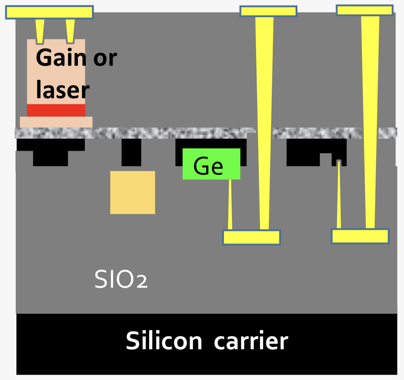
Once the silicon photonics chips are fabricated on a wafer, Scintil’s process bonds the wafer onto a silicon carrier, flips it and etches off the silicon-on-insulator (SOI) substrate.
Indium phosphide is bonded onto the exposed silicon layer before being processed to fabricate such active components as lasers, semiconductor optical amplifiers and hybrid modulators using CMOS fabrication techniques (see image).
Menezo describes the fabrication as CMOS-friendly: standard off-the-shelf processes are used while the processing of III-V is CMOS-compatible in terms of etching and electrical contacts.
Scintil’s process is also scalable, she says: new materials and functions will be added over time to the silicon photonics processes without impacting the integration of III-V materials onto the silicon.
“The more you design these devices and circuits, the more you see the design opportunities you have,” says Menezo. “This is the future if people manage to make it as a friendly as CMOS technology.”
Applications
Scintil Photonics is already working on circuit prototypes with the foundry.
The prototypes include coherent components for optical transmission and designs for 800-gigabit and 1.6-terabyte client-side interfaces. These are based on parallelising existing 400-gigabit DR4 and FR4 designs.
“For an 800-gigabit, the use of eight lanes [each lane being 100 gigabits] is indeed a good target because of [the need for] more integration,” says Menezo. “We can also scale to higher-speed lanes with our hybrid indium phosphide/ silicon photonics modulator.”
Eight-hundred gigabit modules are only needed from 2022 at the earliest.
Another application area for the technology is co-packaged optics, using optical interfaces to move data on- and off-chip.
Menezo says that the company is already thinking about the next round of funding but that it is at least two years away.

ECOC 2019 industry reflections

Gazettabyte is asking industry figures for their thoughts after attending the recent ECOC show, held in Dublin. In particular, what developments and trends they noted, what they learned and what, if anything, surprised them. Here are the first responses from Huawei, OFS Fitel and ADVA.
James Wangyin, senior product expert, access and transmission product line at Huawei
At ECOC, one technology that is becoming a hot topic is machine learning. There is much work going on to model devices and perform optimisation at the system level.
And while there was much discussion about 400-gigabit and 800-gigabit coherent optical transmissions, 200-gigabit will continue to be the mainstream speed for the coming three-to-five years.
That is because, despite the high-speed ports, most networks are not being run at the highest speed. More time is also needed for 400-gigabit interfaces to mature before massive deployment starts.
BT and China Telecom both showed excellent results running 200-gigabit transmissions in their networks for distances over 1,000km.
We are seeing this with our shipments; we are experiencing a threefold year-on-year growth in 200-gigabit ports.
Another topic confirmed at ECOC is that fibre is a must for 5G. People previously expressed concern that 5G would shrink the investment of fibre but many carriers and vendors now agree that 5G will boost the need for fibre networks.
As for surprises at the show, the main discussion seems to have shifted from high-speed optics to system-level or device-level optimisation using machine learning.
Many people are also exploring new applications based on the fibre network.
For example, at a workshop to discuss new applications beyond 5G, a speaker from Orange talked about extending fibre connections to each room, and even to desktops and other devices. Other operators and systems vendors expressed similar ideas.
Verizon discussed, in another market focus talk, its monitoring of traffic and the speed of cars using fibre deployed alongside roads. This is quite impressive.
We are also seeing the trend of using fibre and 5G to create a fully-connected world.
Such applications will likely bring new opportunities to the optical industry.
Two other items to note.
The Next Generation Optical Transport Network Forum (NGOF) presented updates on optical technologies in China. Such technologies include next-generation OTN standardisation, the transition to 200 gigabits, mobile transport and the deployment of ROADMs. The NGOF also seeks more interaction with the global community.
The 800G Pluggable MSA was also present at ECOC. The MSA is also keen for more companies to join.
Daryl Inniss, director, new business development at OFS Fitel
There were many discussions about co-packaged optics, regarding the growth trends in computing and the technology’s use in the communications market.
This is a story about high-bandwidth interfaces and not just about linking equipment but also the technology’s use for on-board optical interconnects and chip-to-chip communications such as linking graphics processing units (GPUs).
I learned that HPE has developed a memory-centric computing system that improves significantly processing speed and workload capacity. This may not be news but it was new to me. Moreover, HPE is using silicon photonics in its system including a quantum dot comb laser, a technology that will come for others.
As for surprises, there was a notable growing interest in spatial-division multiplexing (SDM). The timescale may be long term but the conversations and debate were lively. Two areas to watch are in proprietary applications such as very short interconnects in a supercomputer and for undersea networks where the hyperscalers quickly consume the capacity on any newly commission link.
Lastly, another topic of note was the use of spectrum outside the C-band and extending the C-band itself to increase the data-carrying capacity of the fibre.
Jörg-Peter Elbers, senior vice president, advanced technology, ADVA
Co-packaging optics with electronics is gaining momentum as the industry moves to higher and higher silicon throughput. The advent of 51.2 terabit-per-second (Tbps) top-of-rack switches looks like a good interception point. Microsoft and Facebook also have a co-packaged optics collaboration initiative.
As for coherent, quo vadis? Well, one direction is higher speeds and feeds. What will the next symbol rate be for coherent after 60-70 gigabaud (GBd)? A half-step or a full-step; incremental or leap-frogging? The growing consensus is a full-step: 120-140 GBd.
Another direction for coherent is new applications such as access/ aggregation networks. Yet cost, power and footprint challenges will have to be solved.
Advanced optical packaging, an example being the OIF IC-TROSA project, as well as compact silicon photonics and next-gen coherent DSPs are all critical elements here.
A further issue arising from ECOC is whether optical networks need to deliver more than just bandwidth.
Latency is becoming increasingly important to address time-sensitive applications as well as for advanced radio technologies such as 5G and beyond.
Additional applications are the delivery of precise timing information (frequency, time of day, phase synchronisation) where the existing fibre infrastructure can be used to deliver additional services.
An interesting new field is the use of the communication infrastructure for sensing, with Glenn Wellbrock giving a presentation on Verizon’s work at the Market Focus.
Other topics of note include innovation in fibres and optics for 5G.
With spatial-division multiplexing, interest in multi-core and multi-mode fibre applications have weakened. Instead, more parallel fibres operating in the linear regime appear as an energy-efficient, space-division multiplexing alternative.
Hollow-core fibres are also making progress, offering not only lower latencies but lower nonlinearity compared to standard fibres.
As for optics for 5G, what is clear is that 5G requires more bandwidth and more intelligence at the edge. How network solutions will look will depend on fibre availability and the associated cost.
With eCPRI, Ethernet is becoming the convergence protocol for 5G transport. While grey and WDM (G.metro) optics, as well as next-generation PON, are all being discussed as optical underlay options. Grey and WDM optics offer an unbundling on the fibre/virtual fibre level whereas (TDM-)PON requires bitstream access.
Another observation is that radio “x-haul” [‘x’ being front, mid or back] will continue to play an important role for locations where fibre is nonexistent and uneconomical.
Acacia eyes pluggables as it demos its AC1200 module
The emerging market opportunity for pluggable coherent modules is causing companies to change their strategies.
Ciena is developing and plans to sell its own coherent modules. And now Acacia Communications, the coherent technology specialist, says it is considering changing its near-term coherent digital signal processor (DSP) roadmap to focus on coherent pluggables for data centre interconnect and metro applications.

Source: Gazettabyte
DSP roadmap
Acacia’s coherent DSP roadmap in recent years has alternated between an ASIC for low-power, shorter-reach applications followed by a DSP to address more demanding, long-haul applications.
In 2014, Acacia announced its Sky 100-gigabit DSP for metro applications that was followed in 2015 by its Denali dual-core DSP that powers its 400-gigabit AC-400 5x7-inch module. Then, in 2016, Acacia unveiled its low-power Meru, used within its pluggable CFP2-DCO modules. The high-end 1.2-terabit dual-core Pico DSP used for Acacia’s board-mounted AC1200 coherent module was unveiled in 2017.
“The 400ZR is our next focus,” says Tom Williams, senior director of marketing at Acacia.
The 400ZR standard, promoted by the large internet content providers, is being developed to link switches in separate data centres up to 80km apart. Acacia’s subsequent coherent DSP that follows the 400ZR may also target pluggable applications such as 400-gigabit CFP2-DCO modules that will span metro and metro-regional distances.
“There is a trend to pluggable, not just the 400ZR but the CFP2-DCO [400-gigabit] for metro,” says Williams. “We are still evaluating whether that causes a shift in our overall cadence and DSP development.”
AC1200 trials
Meanwhile, Acacia has announced the results of two transatlantic trials involving its AC1200 module whose production is now ramping.
>
“There is a trend to pluggable, not just the 400ZR but the CFP2-DCO [400-gigabit] for metro”
In the first trial, Acacia, working with ADVA, transmitted a 300-gigabit signal over a 6,800km submarine cable. The 300-gigabit wavelength occupied a 70GHz channel and used ADVA’s Teraflex technology, part of ADVA’s FSP 3000 CloudConnect platform. Teraflex is a one-rack-unit (1RU) stackable chassis that supports three hot-pluggable 1.2-terabit sleds, each sled incorporating an Acacia AC1200 module.
In a separate trial, the AC1200 was used to send a 400-gigabit signal over 6,600km using the Marea submarine cable. Marea is a joint project between Microsoft, Facebook and Telxius that links the US and Spain. The cable is designed for performance and uses an open line system, says Williams: “It is not tailored to a particular company’s [transport] solution”.
The AC1200 module - 40 percent smaller than the 5x7-inch AC400 module - uses Acacia’s patented Fractional QAM (quadrature amplitude modulation) technology. The technology uses probabilistic constellation shaping that allows for non-integer constellations. “Instead of 3 or 4 bits-per-symbol, you can have 3.56 bits-per-symbol,” says Williams.
Acacia’s Fractional QAM also uses an adaptive baud rate. For the trial, the 400-gigabit wavelength was sent using the maximum baud rate of just under 70 gigabaud. Using the baud rate to the full allows a lower constellation to be used for the 400-gigabit wavelength thereby achieving the best optical signal-to-noise ratio (OSNR) and hence reach.
In a second demonstration using the Marea cable, Acacia demonstrated a smaller-width channel in order to maximise the overall capacity sent down the fibre. Here, a lower baud rate/ higher constellation combination was used to achieve a spectral efficiency of 6.41 bits-per-second-per-Hertz (b/s/Hz). “If you built out all the channels [on the fibre], you achieve of the order of 27 terabits,” says Williams.
Pluggable coherent
The 400ZR will be implemented using the same OSFP and QSFP-DD pluggable modules used for 400-gigabit client-side interfaces. This is why an advanced 7nm CMOS process is needed to implement the 400ZR DSP so that its power consumption will be sufficiently low to meet the modules’ power envelopes when integrated with Acacia’s silicon-photonics optics.
There is also industry talk of a ZR+, a pluggable module with a reach exceeding80km. “At ECOC, there was more talk about the ZR+,” says Williams. “We will see if it becomes standardised or just additional proprietary performance.”
Another development is the 400-gigabit CFP2-DCO. At present, the CFP2-DCO delivers up to 200-gigabitwavelengths but the standard, as defined by the Optical Internetworking Forum (OIF), also supports 400 gigabits.
Williams says that there a greater urgency to develop the 400ZR than the 400-gigabit CFP2-DCO. “People would like to ramp the ZR pretty close to the timing of the 400-gigabit client-side interfaces,” says Williams. And that is likely to be from mid-2019.
In contrast, the 400-gigabit CFP2-DCO pluggable while wanted by carriers for metro applications, is not locked to any other infrastructure build-out, says Williams.

Acacia looks to co-package its coherent PIC and DSP-ASIC
- Acacia Communications is working to co-package its coherent DSP and its silicon photonics transceiver chip.
- The company is also developing a digital coherent optics module that will support 400 gigabit.
Acacia Communications is working to co-package its coherent DSP and its silicon photonics transceiver chip. The line-side optical transceiver company is working on a digital coherent optics module that will support 400 gigabits.
Acacia announced last November that it was sampling the industry’s first CFP2 Digital Coherent Optics (CFP2-DCO) that supports 100- and 200-gigabit line rates. The CFP2-DCO integrates the DSP and its silicon photonics chip within a CFP2 module, which is half the size of a CFP module, with each chip packaged separately.
The CFP2-DCO adds to the company’s CFP2-ACO design that was announced a year ago. In the CFP2-ACO, the CFP2 module contains just the optics with the DSP-ASIC chip on the same line card connected to the module via a special high-speed interface connector.
Now, Acacia is working to co-package the two chips, which will not only improve the performance of its CFP2-DCO but also enable new, higher-performance optical modules such as a 400-gigabit DCO. The Optical Internetworking Forum announced a new implementation agreement last December for an interoperable 400-gigabit ZR (80km) coherent interface.
Both [the DSP and silicon photonics chip] are based on CMOS processes. The next step for Acacia is to bring them into a single package.
Portfolio upgrades
Acacia has also upgraded its existing portfolio of coherent transceivers. The company has integrated the enhanced silicon photonics coherent transceiver in its AC100-CFP and its AC-400 5x7-inch modules.
The silicon-photonics transceiver achieves a more efficient coupling of light in and out of the chip and uses an improved modulator driver design that reduces the overall power consumption. The design also supports flexible grid, enabling channel sizes of 37.5GHz in addition to fixed-grid 50GHz channels.
The resulting AC100-CFP module has a greater reach of 2,500km and a lower power consumption than the first generation design announced in 2014. The enhanced PIC has also been integrated within the AC-400. The AC-400, announced in 2015, integrates two silicon photonics chips to support line rates of 200, 300 and 400 gigabits.
CFP2-DCO
Acacia is using the coherent transceiver photonic integrated circuit (PIC), first used in its CFP2-ACO, alongside a new coherent DSP to integrate the optics and DSP within the compact CFP2.
“The third-generation PIC is a mini PIC; in a gold box that is about the size of a dime, which is a third of the size of our original PIC,” says Benny Mikkelsen, founder and CTO of Acacia.
One design challenge with its latest DSP was retaining the reach of the original DSP used in the AC100-CFP while lowering its power consumption. Having an inherently low-power coherent DSP design in the first place is one important factor. Mikkelsen says this is achieved based on several factors such as the DSP algorithms chosen and how they are implemented in hardware, the clock frequencies used within the chip, how the internal busses are implemented, and the choice of bits-per-symbol used for the processing.
The resulting DSP’s power consumption can be further reduced by using an advanced CMOS process. Acacia uses a 16nm CMOS process for its latest DSP.
Other challenges to enable a CFP2-DCO module include reducing the power consumption of the optics and reducing the packaging size. “The modulator driver is the piece part that consumes the most power on the optics side,” says Mikkelsen.
Acacia's CFP2-DCO supports polarisation multiplexing, quadrature phase-shift keying (PM-QPSK) for 100 gigabits, and two modulation schemes: polarisation multiplexing, 8-ary quadrature amplitude multiplexing (PM-8QAM) and 16-ary QAM - for 200-gigabit line rates. In contrast, its -ACO supports just PM-QPSK and PM-16QAM.
At 100 gigabits, the DSP consumes about half the power of the Sky DSP used in the original AC100. Using PM-8QAM for 200 gigabits means the new DSP and optics support a higher baud rate - some 45 gigabaud compared to the traditional 32-35 gigabaud used for 100 and 200-gigabit transmission. However, while this increases the power consumption, the benefit of 8QAM is a 200-gigabit reach beyond 1,000km.
Mikkelsen stresses that a key reason the company can achieve a CFP2-DCO design is having both technologies in-house: “You can co-optimise the DSP and the silicon photonics”.
We think, at least in the near term, that the OSPF module seems to be a good form factor to work on
ACO versus DCO
Since Acacia now offers both the CFP2-ACO and CFP2-DCO modules, it is less concerned about how the relative demand for the two modules develops. “We don’t care too much which one is going to have the majority of the market,” says Mikkelsen. That said, Acacia believes that the CFP2-DCO market will become the larger of the two.
When the CFP2-ACO was first considered several years ago, the systems vendors and optical module makers shared a common interest. Systems vendors wanted to use their custom coherent DSP-ASICs while the -ACO module allowed component makers that didn't have the resources to develop their own DSP to address the market with their optics. It was also necessary to separate the DSP and the optics if the smaller CFP2 form factor was to be used.
But bringing CFP2-ACOs to volume production has proved more difficult than first envisaged. The CFP2-DCO is far easier to use, says Mikkelsen. The module can be plugged straight into equipment whereas the CFP2-ACO must be calibrated by a skilled optical engineer when a wavelength is first turned up.
Future work
Acacia is now looking at new module form factors and new packaging technologies. “Both [the DSP and silicon photonics chip] are based on CMOS processes,” says Mikkelsen. “The next step for Acacia is to bring them into a single package.”
In addition to the smaller size, a single package promises a slightly lower power consumption as well as manufacturing cost advantages. “We also expect to see higher performance once the DSP and optics are sitting next to each other which we believe will improve signal integrity between the two,” says Mikkelsen.
Acacia is not waiting for any industry challenges to be overcome for a single-package design to be achieved. The company points out that its silicon photonics chip is not temperature sensitive, aiding its co-packaging with the DSP.
Acacia is working on a 400-gigabit DCO design and is looking at several potential module types. The company is a member of the OSFP module MSA as well as the Consortium of On-Board Optics (COBO) which has started a coherent working group. “We think, at least in the near term, that the OSPF module seems to be a good form factor to work on,” says Mikkelsen.
NeoPhotonics showcases a CFP2-ACO roadmap to 400G
The company demonstrated the CFP2-ACO module transmitting at 100 gigabit using polarisation multiplexed, quadrature phase-shift keying (PM-QPSK) modulation at the recent OFC show. The line-side module is capable of transmitting over 1,000km and also supports PM-16QAM that doubles capacity over metro network distances.
 Ferris LipscombThe CFP2-ACO is a Class 3 design: the control electronics for the modulator and laser reside on the board, alongside the coherent DSP-ASIC chip.
At OFC, NeoPhotonics also demonstrated single-wavelength 400-gigabit transmission using more advanced modulation and a higher symbol rate, and a short-reach 100-gigabit link for inside the data centre using 4-level pulse-amplitude modulation (PAM4) signalling.
Roadmap to 400 gigabit
One benefit of the CFP2-ACO is that the pluggable module can be deployed only when needed. Another is that the optics will work with coherent DSP-ASICs for different systems vendors and merchant chip suppliers.
“After a lot of technology-bragging about the CFP2-ACO, this is the year it is commercial,” says Ferris Lipscomb, vice president of marketing at NeoPhotonics.
Also demonstrated were the components needed for a next-generation CFP2-ACO: NeoPhotonics’ narrow line-width tunable laser and its higher-bandwidth integrated coherent receiver. To achieve 400 gigabit, 32-QAM and a 45 gigabaud symbol rate were used.
Traditional 100-gigabit coherent uses a 32-gigabaud symbol rate. That combined with QPSK and the two polarisations results in a total bit rate of 2 polarisations x 2bits/symbol x 32 gigabaud or 128 gigabits: a 100-gigabit payload and the rest overhead bits. Using 32-QAM instead of QPSK increases the number of bits encoded per symbol from 2 to 5, while increasing the baud rate from 32 to 45 gigabaud adds a speed-up factor of 1.4. Combining the two, the resulting bit rate is 45 gigabaud x 5bits/symbol x 2 polarisations or 450 gigabit overall.
After a lot of technology-bragging about the CFP2-ACO, this is the year it is commercial
Using 32-QAM curtails the transmission distance to 100km due to the denser constellation but such distances are suited for data centre interconnect applications.
“That was the demo [at OFC] but the product is also suitable for metro distances of 500km using 16-QAM and long-haul of 1,000km using 200 gigabit and 8-QAM,” says Lipscomb.
PAM4
The PAM4 demonstration highlighted NeoPhotonics’ laser and receiver technology. The company showcased a single-wavelength link running at 112 gigabits-per-second using its 56Gbaud externally modulated laser (EML) with an integrated driver. The PAM4 link can span 2km in a data centre.
“What is not quite ready for building into modules is the [56Gbaud to 112 gigabit PAM4] DSP, which is expected to be out in the middle to the second half of the year,” says Lipscomb. The company will develop its own PAM4-based optical modules while selling its laser to other module makers.
Lipscomb says four lanes at 56 gigabaud using PAM4 will deliver a cheaper 400-gigabit solution than eight lanes, each at 25 gigabaud.
Silicon Photonics
NeoPhotonics revealed that it is supplying new 1310nm and 1550nm distributed feedback (DFB) lasers to optical module players that are using silicon photonics for their 100-gigabit mid-reach transceivers. These include the 500m PSM-4, and the 2km CWDM4 and CLR4.
Lipscomb says the benefits of its lasers for silicon photonics include their relatively high output power - 40 to 60mW - and the fact that the company also makes laser arrays which are useful for certain silicon photonics applications.
NeoPhotonics’ laser products have been for 100-gigabit modules with reaches of 2km to 10km. “Silicon photonics is usually used for shorter reaches of a few hundred meters,” says Lipscomb. “This new product is our first one aimed at the short reach data centre market segment.”
“Our main products have been for 100-gigabit modules for the longer reaches of 2km to 10km,” says Lipscomb. “Silicon photonics is usually used for shorter reaches of a few hundred meters, and this new [laser] product is our first one aimed at the short reach data centre market segment."
The company says it has multiple customer engagements spanning various wavelength plans and approaches for Nx100-gigabit data centre transceiver designs. Mellanox Technologies is one vendor using silicon photonics that NeoPhotonics is supplying.
Imec gears up for the Internet of Things economy
It is the imec's CEO's first trip to Israel and around us the room is being prepared for an afternoon of presentations the Belgium nanoelectronics research centre will give on its work in such areas as the Internet of Things and 5G wireless to an audience of Israeli start-ups and entrepreneurs.
 Luc Van den hove
iMinds merger
Imec announced in February its plan to merge with iMinds, a Belgium research centre specialising in systems software and security, a move that will add 1,000 staff to imec's 2,500 researchers.
At first glance, the world-renown semiconductor process technology R&D centre joining forces with a systems house is a surprising move. But for Van den hove, it is a natural development as the company continues to grow from its technology origins to include systems-based research.
"Over the last 15 years we have built up more activities at the system level," he says. "These include everything related to the Internet of Things - our wireless and sensor programmes; we have a very strong programme on biomedical applications, which we sometimes refer to as the Internet of Healthy Things - wearable and diagnostics devices, but always leveraging our core competency in process technology."
Imec is also active in energy research: solar cells, power devices and now battery technology.
For many of these systems R&D programmes, an increasing challenge is managing data. "If we think about wearable devices, they collect data all the time, so we need to build up expertise in data fusion and data science topics," says Van den hove. There is also the issue of data security, especially regarding personal medical data. Many security solutions are embedded in software, says Van den hove, but hardware also plays a role.
Imec expects the Internet of Things to generate massive amounts of data, and more and more intelligence will need to be embedded at different levels in the network
"It just so happens that next to imec we have iMinds, a research centre that has top expertise in these areas [data and security]," says Van den hove. "Rather than compete with them, we felt it made more sense to just merge."
The merger also reflects the emergence of the Internet of Things economy, he says, where not only will there be software development but also hardware innovation: "You need much more hardware-software co-development". The merger is expected to be completed in the summer.
Internet of Things
Imec expects the Internet of Things to generate massive amounts of data, and more and more intelligence will need to be embedded at different levels in the network.
"Some people refer to it as the fog - you have the cloud and then the fog, which brings more data processing into the lower parts of the network," says Van den hove. "We refer to it as the Intuitive Internet of Things with intelligence being built into the sensor nodes, and these nodes will understand what the user needs; it is more than just measuring and sending everything to the cloud."
Van den hove says some in the industry believe that these sensors will be made in cheap, older-generation chip technologies and that processing will be performed in data centres. "We don't think so," he says. "And as we build in more intelligence, the sensors will need more sophisticated semiconductors."
Imec's belief is that the Internet of Things will be a driver for the full spectrum of semiconductor technologies. "This includes the high-end [process] nodes, not only for servers but for sophisticated sensors," he says.
"In the previous waves of innovation, you had the big companies dominating everything," he says. "With the Internet of Things, we are going to address so many different markets - all the industrial sectors will get innovation from the Internet of Things." There will be opportunities for the big players but there will also be many niche markets addressed by start-ups and small to medium enterprises.
Imec's trip to Israel is in response to the country's many start-ups and its entrepreneurship. "Especially now with our wish to be more active in the Internet of Things, we are going to work more with start-ups and support them," he says. "I believe Israel is an extremely interesting area for us in the broad scope of the Internet of Things: in wireless and all these new applications."
 Herzliya
Semiconductor roadmap
Van den hove's background is in semiconductor process technology. He highlights the consolidation going on in the chip industry due, in part, to the CMOS feature nodes becoming more complex and requiring greater R&D expenditure to develop, but this is a story he has heard throughout his career.
"It always becomes more difficult - that is Moore's law - and [chip] volumes compensate for those challenges," says Van den hove. When he started his career 30 years ago the outlook was that Moore's law would end in 10 years' time. "If I talk to my core CMOS experts, the outlook is still 10 years," he says.
Imec is working on 7nm, 5nm and 3nm feature-size CMOS process technologies. "We see a clear roadmap to get there," he says. He expects the third dimension and stacking will be used more extensively, but he does not foresee the need for new materials like graphene or carbon nanotubes being used for the 3nm process node.
Imec is pursuing finFET transistor technology and this could be turned 90 degrees to become a vertical nanowire, he says. "But this is going to be based on silicon and maybe some compound semiconductors like germanium and III-V materials added on top of silicon." The imec CEO believes carbon-based materials will appear only after 3nm.
"The one thing that has to happen is that we have a cost-effective lithography technique and so EUV [extreme ultraviolet lithography] needs to make progress," he says. Here too he is upbeat pointing to the significant progress made in this area in the last year. "I think we are now very close to real introduction and manufacturing," he says.
We see strong [silicon photonics] opportunities for optical interconnect and that is one of our biggest activities, but also sensor technology, particularly in the medical domain
Silicon Photonics
Silicon photonics is another active research area with some 200 staff at imec and at its associated laboratory at Ghent university. "We see strong opportunities for optical interconnect and that is one of our biggest activities, but also sensor technology, particularly in the medical domain," he says.
Imec views silicon photonics as an evolutionary technology. "Photonics is being used at a certain level of a system now and, step by step, it will get closer to the chip," he says. "We are focussing more on when it will be on the board and on the chip."
Van den hove talks about integrating the photonics on a silicon interposer platform to create a cost-effective solution for the printed circuit board and chip levels. For him, first applications of such technology will be at the highest-end technologies of the data centre.
For biomedical sensors, silicon photonics is a very good detector technology. "You can grow molecules on top of the photonic components and by shining light through them you can perform spectroscopy; the solution is extremely sensitive and we are using it for many biomedical applications," he says.
Looking forward, what most excites Van den hove is the opportunity semiconductor technology has to bring innovation to so many industrial sectors: "Semiconductors have created a fantastic revolution is the way we communicate and compute but now we have an opportunity to bring innovation to nearly all segments of industry".
He cites medical applications as one example. "We all know people that have suffered from cancer in our family, if we can make a device that would detect cancer at a very early stage, it would have an enormous impact on our lives."
Van den hove says that while semiconductors is a mature technology, what is happening now is that semiconductors will miniaturise some of the diagnostics devices just like has happened with the cellular phone.
"We are developing a single chip that will allow us to do a full blood analysis in 10 minutes," he says. DNA sequencing will also become a routine procedure when visiting a doctor. "That is all going to be enabled by semiconductor technology."
Such developments is also a reflection of how various technologies are coming together: the combination of photonics with semiconductors, and the computing now available.
Imec is developing a disposable chip designed to find tumour cells in the blood that requires the analysis of thousands of images per second. "The chip is disposable but the calculations will be done on a computer, but it is only with the most advanced technology that you can do that," says Van den hove.
US invests $610 million to spur integrated photonics
 Prof. Duncan Moore
Dubbed the American Institute for Manufacturing Integrated Photonics (AIM Photonics), the venture has attracted 124 partners includes 20 universities and over 50 companies.
The manufacturing innovation institute will be based in Rochester, New York, and will be led by the Research Foundation for the State University of New York. A key goal is that the manufacturing institute will continue after the initiative is completed in early 2021.
We are at the point in photonics where we were in electronics when we still had transistors, resistors and capacitors. What we are trying to do now is the equivalent of the electronics IC
While the focus is on photonic integrated circuits, the expectation is that the venture will end up being broader. “NASA, the Department of Energy and the Department of Defense are all interested in using this as a vehicle for doing other work,” says Duncan Moore, professor of optics at the University of Rochester.
The venture will address such issues as design, on-chip manufacturing, packaging and assembly of PICs. “We are at the point in photonics where we were in electronics when we still had transistors, resistors and capacitors,” says Moore. “What we are trying to do now is the equivalent of the electronics IC.”
"It is an amazing public-private consortium utilizing an unprecedented $610 million investment in photonics," says Richard Soref, a silicon photonics pioneer and a Group IV photonics researcher. "The large and powerful team of world-class investigators is likely to make research-and-development progress of great importance for the US and the world.”
Project plans
The first six months are being used to fill in project’s details. “There are overall budget numbers but individual projects are not well defined in the proposal,” says Moore, adding that many of the subfields - packaging, sensors and the like - will be defined and request-for-proposals issued.
An executive committee will then determine which projects are funded and to what degree. Project durations will vary from one-offs to the full five years.
The large and powerful team of world-class investigators is likely to make research-and-development progress of great importance for the US and the world
Companies backing the project include indium phosphide specialist Infinera as well as silicon photonics players Acacia Communications, Aurrion, and Intel. How the two technologies as well as Group IV photonics will be accommodated as part of the manufacturing base is still to be determined, says Prof. Moore. His expectation is that all will be investigated before a ‘shakeout’ will occur as the venture progresses.
The focus will be on telecom wavelengths and the mid-wave 3 to 5 micron band. “There are a lot of applications in that [longer] wavelength band: remote sensing, environmental analysis, and for doing things on the battlefield,” says Moore.
A public document will be issued around the year-end describing the project’s organisation.
Further information:
The White House factsheet, click here
A Photonics video interview with the chairman of the institute, Professor Robert Clark, click here
Data centres to give silicon photonics its chance
The scale of modern data centres and the volumes of transceivers they will use are going to have a significant impact on the optical industry. So claims Facebook, the social networking company.
 Katharine Schmidtke
Facebook has been vocal in outlining the optical requirements it needs for its large data centres.
The company will use duplex single-mode fibre and has chosen the 2 km mid-reach 100 gigabit CWDM4 interface to connect its equipment.
But the company remains open regarding the photonics used inside transceivers. “Facebook is agnostic to technology,“ says Katharine Schmidtke, strategic sourcing manager, optical technology at Facebook. “There are multiple technologies that meet our requirements.”
That said, Facebook says silicon photonics has characteristics that are appealing.
Silicon photonics can produce integrated designs, with all the required functions placed in one or two chips. Such designs will also be needed in volume, given that a large data centre uses hundred of thousands of optical transceivers, and that requires a high-yielding process. This is a manufacturing model the chip industry excels at, and one that silicon photonics, which uses a CMOS-compatible process, can exploit.
When you bring up a data centre, you don’t just deploy, you deploy a data centre
New business model
What data centres brings to optics is scale. Optical transceiver volumes used by data centres are growing, and growing fast, and will account for half the industry’s demand for Ethernet transceivers by 2020, according to LightCounting Market Research.
Transceivers must be designed with high-volume, low-cost manufacturing in mind from the start. This is different to what the market has done traditionally. “With the telecom industry, you step into volume in more manageable, digestible chunks,” says Schmidtke. “When you bring up a data centre, you don’t just deploy, you deploy a data centre.”
Silicon photonics has already proven it can achieve the required optical performance, says Facebook, what remains open is whether the technology can meet the manufacturing demands of the data centre. What helps its cause is that the data centre provides the volumes needed to achieve such a manufacturing maturity.
Schmidtke is upbeat about silicon photonics’ prospects.
“Why silicon photonics is attractive is integration; you are reducing the number of components and the bill of materials significantly, and that reduces cost,” she says. “Then there is all the alignment and assembly cost reductions; that is what makes this technology appealing.”
Her expectation is that the industry will demonstrate the required level of manufacturing maturity in the coming year. Then the role silicon photonics will play for this market will become clearer.
“Within a year it will be very obvious,” she says.
Verizon tips silicon photonics as a key systems enabler
Part 3: An operator view
Glenn Wellbrock is upbeat about silicon photonics’ prospects. Challenges remain, he says, but the industry is making progress. “Fundamentally, we believe silicon photonics is a real enabler,” he says. “It is the only way to get to the densities that we want.”
 Glenn Wellbrock
Wellbrock adds that indium phosphide-based photonic integrated circuits (PICs) can also achieve such densities.
But there are many potential silicon photonics suppliers because of its relatively low barrier to entry, unlike indium phosphide. "To date, Infinera has been the only real [indium phosphide] PIC company and they build only for their own platform,” says Wellbrock.
That an operator must delve into emerging photonics technologies may at first glance seem surprising. But Verizon needs to understand the issues and performance of such technologies. “If we understand what the component-level capabilities are, we can help drive that with requirements,” says Wellbrock. “We also have a better appreciation for what the system guys can and cannot do.”
Verizon can’t be an expert in the subject, he says, but it can certainly be involved. “To the point where we understand the timelines, the cost points, the value-add and the risk factors,” he says. “There are risk factors that we also want to understand, independent of what the system suppliers might tell us.”
The cost saving is real, but it is also the space savings and power saving that are just as important
All the silicon photonics players must add a laser in one form or another to the silicon substrate since silicon itself cannot lase, but pretty much all the other optical functions can be done on the silicon substrate, says Wellbrock: “The cost saving is real, but it is also the space savings and power saving that are just as important.”
The big achievement of silicon photonics, which Wellbrock describes as a breakthrough, is the getting rid of the gold boxes around the discrete optical components. “How do I get to the point where I don’t have fibre connecting all these discrete components, where the traces are built into the silicon, the modulator is built in, even the detector is built right in.” The resulting design is then easier to package. “Eventually I get to the point where the packaging is glass over the top of that.”
So what has silicon photonics demonstrated that gives Verizon confidence about its prospects?
Wellbrock points to several achievements, the first being Infinera’s PICs. Yes, he says, Infinera’s designs are indium phosphide-based and not silicon photonics, but the company makes really dense, low-power and highly reliable components.
He also cites Cisco’s silicon photonics-based CPAK 100 Gig optical modules, and Acacia, which is applying silicon photonics and its in-house DSP-ASICs to get a lower power consumption than other, high-end line-side transmitters.
Verizon believes the technology will also be used in CFP4 and QSFP28 optical modules, and at the next level of integration that avoids pluggable modules on the equipment's faceplate altogether.
But challenges remain. Scale is one issue that concerns Verizon. What makes silicon chips cheap is the fact that they are made in high volumes. “It [silicon photonics] couldn’t survive on just the 100 gigabit modules that the telecom world are buying,” says Wellbrock.
If these issues are not resolved, then indium phosphide continues to win for a long time because that is where the volumes are today
When Verizon asks the silicon photonics players about how such scale will be achieved, the response it gets is data centre interconnect. “Inside the data centre, the optics is growing so rapidly," says Wellbrock. "We can leverage that in telecom."
The other issue is device packaging, for silicon photonics and for indium phosphide. It is ok making a silicon-photonics die cheaply but unless the packaging costs can be reduced, the overall cost saving is lost. ”How to make it reliable and mainstream so that everyone is using the same packaging to get cost down,” says Wellbrock.
All these issues - volumes, packaging, increasing the number of applications a single part can be applied to - need to be resolved and almost simultaneously. Otherwise, the technology will not realise its full potential and the start-ups will dwindle before the problems are fixed.
“If these issues are not resolved, then indium phosphide continues to win for a long time because that is where the volumes are today,” he says.
Verizon, however, is optimistic. “We are making enough progress here to where it should all pan out,” says Wellbrock.
The quiet period of silicon photonics
Michael Hochberg discusses his book on silicon photonics and the status of the technology. Hochberg is director of R&D at Coriant's Advanced Technology Group. Previously he has been an Associate Professor at the University of Delaware and at the National University of Singapore. He was also a director at the Optoelectronic Systems Integration in Silicon (OpSIS) foundry, and was a co-founder of silicon photonics start-up, Luxtera.
Part 2: An R&D perspective
If you are going to write a book on silicon photonics, you might as well make it different. That is the goal of Michael Hochberg and co-author Lukas Chrostowski, who have published a book on the topic.
 Michael HochbergHochberg says there is no shortage of excellent theoretical textbooks and titles that survey the latest silicon photonics research. Instead, the authors set themselves the goal of creating a design manual to help spur a new generation of designers.
The book aims to provide designers with all the necessary tools and know-how to develop silicon photonics circuits without needing to be specialists in optics.
“One of the limiting factors in terms of the growth and success of the field is how quickly can we breed up more and more designers,” says Hochberg.
The book - Silicon Photonics Design: From Devices to Systems - starts by exploring the main silicon photonics building blocks, from optical waveguides and grating couplers to modulators, photo-detectors and lasers. The book then addresses putting the parts together, with chapters on tools, fabrication, testing and packaging before finishing with system design examples.
The numerical tools used in the book are mostly based on the finite-difference time-domain method, what the authors describe as the typical workhorse in silicon photonics design. Hochberg admits that the systems software tools, in contrast, are less mature: “It is a moving target that will change year to year.”
Myths
Hochberg is also a co-author of a Nature Photonics’ paper, published in 2012, that debunks some of the myths regarding silicon photonics. “We wrote the myths paper after seeing an upswing in the ratio of hype-to-results going on,” says Hochberg.
He says part of the problem was that people were claiming silicon photonics was going to solve problems that it was plainly unsuited to address, for example integrating photonics with cutting-edge ultra-scale sub-micron electronics, for instance at 16 nm and 28 nm nodes. “That is not a practical solution for any near term problem,” says Hochberg.
More recent events, such as Intel’s announcement in February that it is delaying the commercial introduction of its silicon photonics products, highlights how bringing the technology to market is a significant engineering challenge. Instead, we are in a quiet period for silicon photonics, he says. Companies are getting into serious product mode, where they stop publishing and start focussing on building a product.
Moreover, these products - what he refers to as second-generation silicon photonics designs - are increasingly sophisticated with more functions or channels placed on the chip. “It is the standard story of almost any technology in silicon,” he says. “Silicon wins when you can do more stuff on a single chip.”
Silicon photonics and III-V
Hochberg stresses that while it is an understandable desire, it is very hard to compare the performance of silicon photonics as a whole with traditional optical components using III-V compounds. The issue being that silicon photonics comprises many different platforms where designers have made tradeoffs. The same applies to III-V compounds where there are hundreds of processes aimed at thousands of different products. “It is very hard to compare them in a generic way,” he says.
“The great advantage silicon photonics gives you is access to first-rate fabrication infrastructure,” says Hochberg. Silicon photonics offers 8- and 12-inch wafers, high volume foundries, high process control, the ability to ramp to high volumes and achieve high yields of complex-structure designs with hundreds, even thousands of components on-chip.
In contrast, III-V materials such as indium phosphide and gallium arsenide offer higher mobilities - electrons and holes move faster - and, unlike silicon, can straightforwardly emit light.
“The downside is that III-V foundries use technology processes that silicon stopped using 20 to 30 years ago,” says Hochberg. Wafers that are 2-, 3- or 4-inch in diameter, lithography that is ten times coarser than is used for silicon, process controls that are less advanced, and less automation.
If you are going to design a complex chip with lots of different components that require a predictable relationship with each other, this is where silicon tends to beat III-Vs, he says.
But the claim of large silicon wafers and huge volumes is what silicon photonics proponents have been promoting for years, and which has fed some of the false expectation associated with the emerging technology, says one industry analyst.
Hochberg counters by highlighting two trends that play in silicon photonics’ favour.
One is the well-known one of optics slowly replacing copper. This has been going on for 40 to 50 years, he says, in long haul, then in metro and now linking equipment in the data centre. “This will continue for shorter and shorter distances and then, at some point, stop,” he says. That said, Hochberg stresses that there are other applications for silicon photonics besides data communications.
“Just because you run out of opportunities at shorter and shorter reach at some point in the distant future, doesn't mean that the field collapses,” he says. “There's a lot of other cool stuff being done in silicon photonics these days with serious commercial potential.” Example applications include medical and remote sensing.
Once you can do something in silicon and do it adequately well, it tends to displace everything else from the majority of the market
The second trend he highlights is that silicon ends up dominating fields, not necessarily because it is the best choice in terms of performance but because it ends up being so cheap in scale. “Once you can do something in silicon and do it adequately well, it tends to displace everything else from the majority of the market.”
There are up-front costs of getting silicon photonics into a CMOS fab so companies have to be judicious in choosing the applications they tackle. “But once the infrastructure gets going to make a new application, the speed with which the industry can scale is just mind-blowing,” he said.
At Coriant, Hochberg leads a team that is doing advanced R&D. “We are doing advanced research with the goal to develop new technology that may eventually make its way into product.”
Does that include silicon photonics? “There is certainly an interest in silicon photonics; it is one of the things we are exploring,” says Hochberg.
Further reading:
Book: Michael Hochberg and Lukas Chrostowski, Silicon Photonics Design: From Devices to Systems, Cambridge University Press, 2015
Paper: Myths and rumours of silicon photonics, Nature Photonics, Vol 6, April 2012.