
Silicon photonics: "The excitement has gone"
The opinion of industry analysts regarding silicon photonics is mixed at best. More silicon photonics products are shipping but challenges remain.
Part 1: An analyst perspective
"The excitement has gone,” says Vladimir Kozlov, CEO of LightCounting Market Research. “Now it is the long hard work to deliver products.”
 Dale Murray, LightCounting
However, he is less concerned about recent setbacks and slippages for companies such as Intel that are developing silicon photonics products. This is to be expected, he says, as happens with all emerging technologies.
Mark Lutkowitz, principal at consultancy fibeReality, is more circumspect. “As a general rule, the more that reality sets in, the less impressive silicon photonics gets to be,” he says. “The physics is just hard; light is not naturally inclined to work on the silicon the way electronics does.”
LightCounting, which tracks optical component and modules, says silicon photonics product shipments in volume are happening. The market research firm cites Cisco’s CPAK transceivers, and 40 gigabit PSM4 modules shipping in excess of 100,000 units as examples. Six companies now offer 40 gigabit PSM4 products with Luxtera, a silicon photonics player, having a healthy start on the other five.
Indium phosphide and other technologies will not step back and give silicon photonics a free ride
LightCounting also cites Acacia with its silicon photonics-based low-power 100 and 400 gigabit coherent modules. “At OFC, Acacia made a fairly compelling case, but how much of its modules’ optical performance is down to silicon photonics and how much is down to its advanced coherent DSP chip is unclear,” says Dale Murray, principal analyst at LightCounting. Silicon photonics has not shown itself to be the overwhelming solution for metro/ regional and long-haul networks to date but that could change, he says.
Another trend LightCounting notes is how PAM-4 modulation is becoming adopted within standards. PAM-4 modulates two bits of data per symbol and has been adopted for the emerging 400 Gigabit Ethernet standard. Silicon photonics modulators work really well with PAM-4 and getting it into standards benefits the technology, says LightCounting. “All standards were developed around indium phosphide and gallium arsenide technologies until now,” says Kozlov.
You would be hard pressed to find a lot of OEMs or systems integrators that talk about silicon photonics and what impact it is going to have
Silicon photonics has been tainted due to the amount of hype it has received in recent years, says Murray. Especially the claim that optical products made in a CMOS fabrication plant will be significantly cheaper compared to traditional III-V-based optical components.
First, Murray highlights that no CMOS production line can make photonic devices without adaptation. “And how many wafers starts are there for the whole industry? How much does a [CMOS] wafer cost?” he says.
“You would be hard pressed to find a lot of OEMs or systems integrators that talk about silicon photonics and what impact it is going to have,” says Lutkowitz. “To me, that has always said everything.”
![]() Mark Lutkowitz, fibeReality LightCounting highlights heterogeneous integration as one promising avenue for silicon photonics. Heterogeneous integration involves bonding III-V and silicon wafers before processing the two.
Mark Lutkowitz, fibeReality LightCounting highlights heterogeneous integration as one promising avenue for silicon photonics. Heterogeneous integration involves bonding III-V and silicon wafers before processing the two.
This hybrid approach uses the III-V materials for the active components while benefitting from silicon’s larger (300 mm) wafer sizes and advanced manufacturing techniques.
Such an approach avoids the need to attach and align an external discrete laser. “If that can be integrated into a WDM design, then you have got the potential to realise the dream of silicon photonics,” says Murray. “But it’s not quite there yet.”
This poses a real challenge for silicon photonics: it will only achieve low cost if there are sufficient volumes, but without such volumes it will not achieve a cost differential
Murray says over 30 vendors now make modules at 40 gigabit and above: “There are numerous module types and more are being added all the time.” Then there is silicon photonics which has its own product pie split. This poses a real challenge for silicon photonics: it will only achieve low cost if there are sufficient volumes, but without such volumes it will not achieve a cost differential.
“Indium phosphide and other technologies will not step back and give silicon photonics a free ride, and are going to fight it,” says Kozlov. Nor is it just VCSELs that are made in high volumes.
LightCounting expects over 100 million indium phosphide transceivers to ship this year. Many of these transceivers use distributed feedback (DFB) lasers and many are at 10 gigabit and are inexpensive, says Kozlov.
For FTTx and GPON, bi-directional optical subassemblies (BOSAs) now cost $9, he says: “How much lower cost can you get?”
Altera’s 30 billion transistor FPGA
- The Stratix 10 features a routing architecture that doubles overall clock speed and core performance
- The programmable family supports the co-packaging of transceiver chips to enable custom FPGAs
- The Stratix 10 family supports up to 5.5 million logic elements
- Enhanced security features stop designs from being copied or tampered with
Altera has detailed its most powerful FPGA family to date. Two variants of the Stratix 10 family have been announced: 10 FPGAs and 10 system-on-chip (SoC) devices that include a quad-core 64-bit architecture Cortex-A53 ARM processor alongside the programmable logic. The ARM processor can be clocked at up to 1.5 GHz.
The Stratix 10 family is implemented using Intel’s 14nm FinFET process and supports up to 5.5 million logic elements. The largest device in Altera’s 20nm Arria family of FPGAs has 1.15 million logic elements, equating to 6.4 billion transistors. “Extrapolating, this gives a figure of some 30 billion transistors for the Stratix 10,” says Craig Davis, senior product marketing manager at Altera.
 Altera's HyperFlex routing architecture. Shown (pointed to by the blue arrow) are the HyperFlex registers that sit at the junction of the interconnect traces. Also shown are the adaptive logic module blocks. Source: Altera.
The FPGA family uses a routing fabric, dubbed HyperFlex, to connect the logic blocks. HyperFlex is claimed to double the clock speed compared to designs implemented using Altera’s Stratix V devices, to achieve gigahertz rates. “Having that high level of performance allows us to get to 400 gigabit and one terabit OTN (Optical Transport Network) systems,” says Davies.
The FPGA company detailed the Stratix 10 a week after Intel announced its intention to acquire Altera for US $16.7 billion.
Altera is also introducing with the FPGA family what it refers to as heterogeneous 3D system packaging and integration. The technology enables a designer to customise the FPGA’s transceivers by co-packaging separate transceiver integrated circuits (ICs) alongside the FPGA.
Different line-rate transceivers can be supported to meet a design's requirements: 10, 28 or 56 gigabit-per-second (Gbps), for example. It also allows different protocols such as PCI Express (PCIe), and different modulation formats including optical interfaces. Altera has already demonstrated a prototype FPGA co-packaged with optical interfaces, while Intel is developing silicon photonics technology.
HyperFlex routing
The maximum speed an FPGA design can be clocked is determined by the speed of its logic and the time it takes to move data from one part of the chip to another. Increasingly, it is the routing fabric rather than the logic itself that dictates the total delay, says Davis.
This has led the designers of the Stratix 10 to develop the HyperFlex architecture that adds a register at each junction of the lines interconnecting the logic elements.
Altera first tackled routing delay a decade ago by redesigning the FPGA’s logic building block. Altera went from a 4-input look-up table logic building block to a more powerful 8-input one that includes output registers. Using the more complex logic element - the adaptive logic module (ALM) - simplifies the overall routing. “You are essentially removing one layer of routing from your system,” says Davies.
When an FPGA is programmed, the file is presented that dictates how the wires and hence the device’s logic are connected. The refinement with HyperFlex is that there are now registers at those locations where the switching between the traces occurs. A register can either be bypassed or used.
“It allows us to put the registers anywhere in the design, essentially placing them in an optimum place for a given route across the FPGA,” says Davies. The number of hyper-registers in the device's routing outnumber the standard registers in the ALM blocks by a factor of ten.
Using the registers, designers can introduce data pipelining to reduce overall delay and it is this pipelining, combined with the advanced 14nm CMOS process, that allows a design to run at gigahertz rates.
“We have made the registers small but they add one or two percent to the total die area, but in return it gives us the ability to go to twice the performance,” says Davies. “That is a good trade-off.
The biggest change getting HyperFlex to work has been with the software tools, says Davies. HyperFlex and the associated tools has taken over three years to develop.
“This is a fundamental change,” says Davies. “It [HyperFlex] is relatively simple but it is key; and it is this that allows customers to get to this doubling of core performance.”
The examples cited by Altera certainly suggest significant improvements in speed, density, power dissipation, but I want to see that in real-world designs
Loring Wirbel, The Linley Group
Applications
Altera says that over 100 customer designs have now been processed using the Stratix 10 development tools.
It cites as an example a current 400 gigabit design implemented using a Stratix V FPGA that requires a bus 1024-bits wide, clocked at 390MHz. The wide bus consumes considerable chip area and routing it to avoid congestion is non-trivial.
Porting the design to a Stratix 10 enables the bus to be clocked at 781MHz such that the bus width can be halved to 512 bits. “It reduces congestion, makes it easier to do timing closure and ship the design,” says Davies. “This is why we think Stratix 10 is so important for high-performance applications like OTN and data centres.” Timing closure refers to the tricky part of a design where the engineer may have to iterate to ensure that a design meets all the timing requirements.
For another, data centre design, a Stratix 10 device can replace five Stratix V ICs on one card. The five FPGAs are clocked at 250MHz, run PCIe Gen2 x8 interfaces and DDR3 x72 memory clocked at 800MHz. Overall the power consumed is 120W. Using one Stratix 10 chip clocked at 500MHz, faster PCIe Gen3 x8 can be supported as can a wider DDR3 x144 memory clocked at 1.2GHz, with only 44W consumed.
Loring Wirbel, senior analyst at The Linley Group, says that Altera’s insertion of pipelined registers to cut average trace lengths is unique.
“The more important question is, can the hyper-register topology regularly gain the type of advantages claimed?” says Wirbel. “The examples cited by Altera certainly suggest significant improvements in speed, density, power dissipation, but I want to see that in real-world designs.”
We are also looking at optical transceivers directly connected to the FPGA
Craig Davies, Altera
Connectivity tiles
Altera recognises that future FPGAs will support a variety of transceiver types. Not only are there different line speeds to be supported but also different modulation schemes. “You can’t build one transceiver that fits all of these requirements and even if you could, it would not be an optimised design,” says Davies.
Instead, Altera is exploiting Intel’s embedded multi-die interconnect bridge (EMIB) technology to interface the FPGA and transceivers, dubbed connectivity tiles. The bridge technology is embedded into the chip’s substrate and enables dense interconnect between the core FPGA and the transceiver IC.
Intel claims fewer wafer processing steps are required to make the EMIB compared to other 2.5D interposer processes. An interposer is an electrical design that provides connectivity. “This is a very simple ball-grid sort of interposer, nothing like the Xilinx interposer,” says Wirbel. “But it is lower cost and not intended for the wide range of applications that more advanced interposers use.”
Using this approach, a customer can add to their design the desired interface, including optical interfaces as well as electrical ones. “We are also looking at optical transceivers directly connected to the FPGA,” says Davies.
Wirbel says such links would simplify interfacing to OTN mappers, and data centre designs that use optical links between racks and for the top-of-rack switch.
“Intel wants to see a lot more use of optics directly on the server CPU board, something that the COBO Alliance agrees with in part, and they may steer the on-chip TOSA/ ROSA (transmitter and receiver optical sub-assembly) toward intra-board applications,” he says.
But this is more into the future. “It's fine if Intel wants to pursue those things, but it should not neglect common MSAs for OTN and Ethernet applications of a more traditional sort,” says Wirbel.
The benefit of the system-in-package integration is that different FPGAs can be built without having to create a new expensive mask set each time. “You can build a modular lego-block FPGA and all that it has different is the packaged substrate,” says Davies.
Security and software
Stratix 10 also features security features to protect companies’ intellectual property from being copied or manipulated.
The FPGA features security hardware that protects circuitry from being tampered with; the bitstream that is loaded to configure the FPGA must be decrypted first.
The FPGA is also split into sectors such that parts of the device can have different degrees of security. The sectoring is useful for cloud-computing applications where the FPGA is used as an accelerator to the server host processor. As a result, different customers’ applications can be run in separate sectors of the FPGA to ensure that they are protected from each other.
The security hardware also allows features to be included in a design that the customer can unlock and pay for once needed. For example, a telecom platform could be upgraded to 100 Gigabit while the existing 40 Gig live network traffic runs unaffected in a separate sector.
Altera has upgraded its FPGA software tools in anticipation of the Stratix 10. Features include a hierarchical design flow to simplify the partitioning of a design project across a team of engineers, and the ability to use cloud computing to speed up design compilation time.
What applications will require such advanced FPGAs, and which customers will be willing to pay a premium price for? Wirbel says the top applications will remain communications.
“The emergence of new 400 Gig OTN transport platforms, and the emergence of all kinds of new routers and switches with 400 Gig interfaces, will keep a 40 percent communication base for FPGAs overall solid at Altera,” he says.
Wirbel also expects server accelerator boards where FPGA-based accelerators are used for such applications as financial trading and physics simulation will also be an important market. “But Intel must consider the accelerator board market as an ideal place for Stratix 10 on its own, and not merely as a vehicle for promoting a future Xeon-plus-FPGA hybrid,” he says.
Altera will have engineering samples of the Stratix 10 towards the end of 2015, before being shipped to customers.
OFC 2015 digest: Part 2
- CFP4- and QSFP28-based 100GBASE-LR4 announced
- First mid-reach optics in the QSFP28
- SFP extended to 28 Gigabit
- 400 Gig precursors using DMT and PAM-4 modulations
- VCSEL roadmap promises higher speeds and greater reach
Acacia unveils 400 Gigabit coherent transceiver
- The AC-400 5x7 inch MSA transceiver is a dual-carrier design
- Modulation formats supported include PM-QPSK, PM-8-QAM and PM-16-QAM
- Acacia’s DSP-ASIC is a 1.3 billion transistor dual-core chip
Acacia Communications has unveiled the industry's first flexible rate transceiver in a 5x7-inch MSA form factor that is capable of up to 400 Gigabit transmission rates. The company made the announcement at the OFC show held in Los Angeles.
Dubbed the AC-400, the transceiver supports 200, 300 and 400 Gigabit rates and includes two silicon photonics chips, each implementing single-carrier optical transmission, and a coherent DSP-ASIC. Acacia designs its own silicon photonics and DSP-ASIC ICs.
"The ASIC continues to drive performance while the optics continues to drive cost leadership," says Raj Shanmugaraj, Acacia's president and CEO.
The AC-400 uses several modulation formats that offer various capacity-reach options. The dual-carrier transceiver supports 200 Gig using polarisation multiplexing, quadrature phase-shift keying (PM-QPSK) and 400 Gig using 16-quadrature amplitude modulation (PM-16-QAM). The 16-QAM option is used primarily for data centre interconnect for distances up to a few hundred kilometers, says Benny Mikkelsen, co-founder and CTO of Acacia: "16-QAM provides the lowest cost-per-bit but goes shorter distances than QPSK."
Acacia has also implemented a third, intermediate format - PM-8-QAM - that improves reach compared to 16-QAM but encodes three bits per symbol (a total of 300 Gig) instead of 16-QAM's four bits (400 Gig). "8-QAM is a great compromise between 16-QAM and QPSK," says Mikkelsen. "It supports regional and even long-haul distances but with 50 percent higher capacity than QPSK." Acacia says one of its customer will use PM-8-QAM for a 10,000 km submarine cable application.
 Source: Gazettabyte
Other AC-400 transceiver features include OTN framing and forward error correction. The OTN framing can carry 100 Gigabit Ethernet and OTU4 signals as well as the newer OTUc1 format that allows client signals to be synchronised such that a 400 Gigabit flow from a router port can be carried, for example. The FEC options include a 15 percent overhead code for metro and a 25 percent overhead code for submarine applications.
The 28 nm CMOS DSP-ASIC features two cores to process the dual-carrier signals. According to Acacia, its customers claim the DSP-ASIC has a power consumption less than half that of its competitors. The ASIC used for Acacia’s AC-100 CFP pluggable transceiver announced a year ago consumes 12-15W and is the basis of its latest DSP design, suggesting an overall power consumption of 25 to 30+ Watts. Acacia has not provided power consumption figures and points out that since the device implements multiple modes, the power consumption varies.
The AC-400 uses two silicon photonics chips, one for each carrier. The design, Acacia's second generation photonic integrated circuit (PIC), has a reduced insertion loss such that it can now achieve submarine transmission reaches. "Its performance is on a par with lithium niobate [modulators]," says Mikkelsen.
It has been surprising to us, and probably even more surprising to our customers, how well silicon photonics is performing
The PIC’s basic optical building blocks - the modulators and the photo-detectors - have not been changed from the first-generation design. What has been improved is how light enters and exits the PIC, thereby reducing the coupling loss. The latest PIC has the same pin-out and fits in the same gold box as the first-generation design. "It has been surprising to us, and probably even more surprising to our customers, how well silicon photonics is performing," says Mikkelsen.
Acacia has not tried to integrate the two wavelength circuits on one PIC. "At this point we don't see a lot of cost savings doing that," says Mikkelsen. "Will we do that at some point in future? I don't know." Since there needs to be an ASIC associated with each channel, there is little benefit in having a highly integrated PIC followed by several discrete DSP-ASICs, one per channel.
The start-up now offers several optical module products. Its original 5x7 inch AC-100 MSA for long-haul applications is used by over 10 customers, while it has two 5x7 inch modules for submarine operating at 40 Gig and 100 Gig are used by two of the largest submarine network operators. Its more recent AC-100 CFP has been adopted by over 15 customers. These include most of the tier 1 carriers, says Acacia, and some content service providers. The AC-100 CFP has also been demonstrated working with Fujitsu Optical Components's CFP that uses NTT Electronics's DSP-ASIC. Acacia expects to ship 15,000 AC-100 coherent CFPs this year.
Each of the company's module products uses a custom DSP-ASIC such that Acacia has designed five coherent modems in as many years. "This is how we believe we out-compete the competition," says Shanmugaraj.
Meanwhile, Acacia’s coherent AC-400 MSA module is now sampling and will be generally available in the second quarter.
Q&A with Richard Soref - Final Part
In the final part of the interview with Gazettabyte, Richard Soref talks about hybrid and monolithic integration, mid-infrared optics, how his photonics predictions made in a 2006 paper have fared, 2-micron-based optical communications, and his talk at OFC in March.
 "In a rosy future, every smart phone, tablet, wrist watch, and hand-held device would contain one of these chemical-medical-physical sensors."
Richard Soref
Q: The distinction between monolithic and hybrid integration? Arguably all silicon photonics is hybrid integration.
RS: Silicon photonics is mostly monolithic and that is its advantage. Hybrid integration occurs when structures from two different material systems are combined, usually by bonding. When describing the construction of silicon photonics, if we include the germanium laser on silicon, then it is possible to make every component in a chip network from Group IV materials, and this qualifies as monolithic integration.
How important is optical performance using either hybrid or a monolithic design? Is this an academic question or are there differences and hence issues to consider when making a device monolithically or hybridly?
RS: There are real-world issues to consider when evaluating the relative performance of hybrid and monolithic. I don’t know whether hybrid integration is CMOS-foundry-compatible but I suspect that it is. I feel that hybrid integration of III-V laser diodes on silicon or germanium is quite practical, both for telecom and mid infrared. The heterogeneous approach is an excellent, viable solution until germanium-tin (GeSn) laser diodes come along.
Considerable investment is required to make monolithic real. Once actual, it should be more cost-effective than hybrid. The definition of monolithic has vague areas. Is epitaxial growth of III-V on silicon monolithic? Perhaps. If you bond a Group IV nano-membrane onto silicon or germanium, is that monolithic? Probably. We need clearer terminology.
The comparison you’re asking for probably comes down to a performance comparison of III-V and Group IV laser diodes and photo-detectors.
Regarding the economics of silicon photonics, one important issue is the cost of silicon photonics compared to copper. This looks like a major factor limiting silicon photonics adoption. Do you have a view on cost?
RS: These economics are outside my areas of expertise, but I’ll take a stab at it.
Active optical cables are one of several possible killer applications of silicon photonics I don’t know the actual numbers but am guessing that the photonic cost is already below the copper coax cost and is capable of further reduction. Data centres are validating silicon photonics adoption.
A general proposition is that ubiquitous photonics could improve our lives. Mass production at very low cost is on the horizon for silicon photonic integrated circuits (PICs). Once the high-volume, high-impact applications are known, the factory can target them. The global silicon infrastructure could push silicon PICs into the lead. Job creation, industrial competitiveness and other benefits to society will flow from high-yield PICs and opto-electronic integrated circuits (OEICs) made on large wafers. Niche applications and boutique chips may offer important functionality but at higher costs, and for those the silicon may not compete well with III-Vs.
In your paper, The Past, Present and Future of Silicon Photonics, published in 2006, you say that no one can foresee the future and that all one can do is make educated guesses. You then go on and make the following predictions shown in the table below.
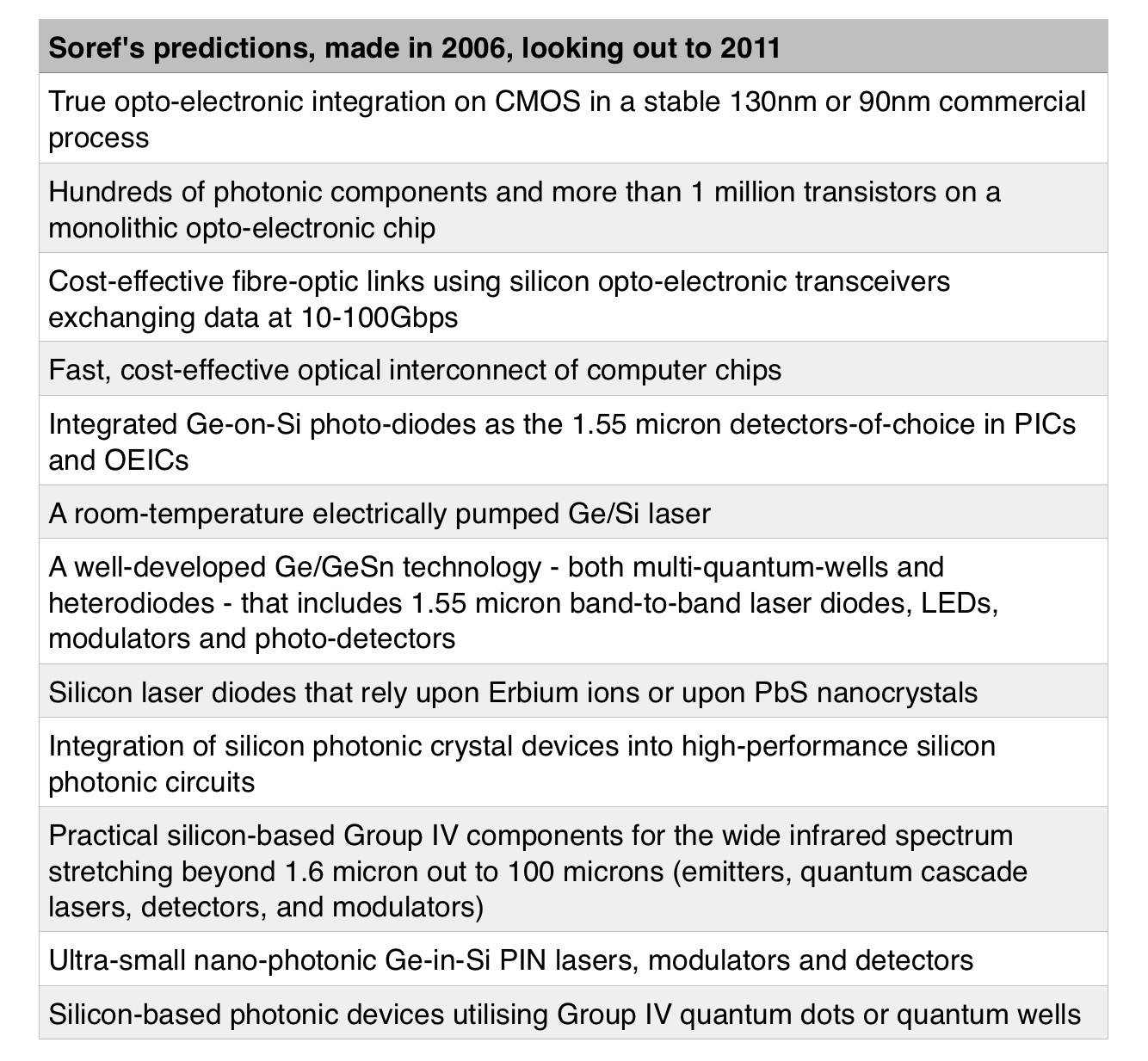
What comments do you have, given the benefit of hindsight?
RS: Well, the scorecard is mixed on these prognostications. A few came true, some are on the verge, others are stuck such as the Erbium-silicon and lead-sulphide-silicon lasers. The mega-transistor OEIC has not yet arrived. The germanium-on-silicon heterolaser diode came true. The high threshold of this laser can be reduced by adding tensile strain and germanium quantum wells, but even after that has been done I feel that this laser’s efficiency will not match that of its III-V competitors.
Efficiency prospects are better for germanium-tin (GeSn). The optically-pumped GeSn laser was just demonstrated in Germany and now we are close to the monolithic on-chip germanium-tin laser diode, although it will emit at 2 microns instead of 1.55 microns.
When I read the press releases of Intel, Cisco, IBM, Mellanox, Luxtera, STMicroelectronics, PhotonIC, IME and imec, I get the impression that major progress has been made in commercial 100 Gigabit-per-second transceiver chips and active optical cables, all of these using hybrid light sources and the germanium photodiodes that I predicted.
Looking at the wide infrared spectrum, the predicted results from 5 to 100 microns have not materialised. However, results are excellent in the 1.6 to 5 micron range. The wavelength-scale components are still on the wanted list, although such modulators and detectors have appeared with a plasmonic flavour.
The GeSn quantum wells arrived in Ghent, Belgium in 2012 and were explored further in Stuttgart, Germany. I believe that a fully fledged silicon-germanium-tin (SiGeSn) technology is unfolding before our eyes today.
The competence of Group IV photonics in so many different scientific areas is its strength and survival mechanism.
In your Photonics West talk in 2013, you talk about silicon opto-electronic mid-infrared system-on-chip. You highlight several interesting application areas including chemical-bio-physical sensing, medical diagnostics, environmental monitoring and high-speed comms at 2 micron. Is sensing a distinct category, and if so, how does it differ from medical diagnostics and environmental monitoring?
RS: Medical diagnostics, industrial process control, and environmental monitoring are all within the same sensing category as chem-bio-physical sensing. That’s why on-chip sensing via photonic techniques is a very broad category. Over time, commercial sales of these photonic sensors - including disposables - could eclipse those of optical interconnects.
How should these mid-infrared applications be seen alongside SiP for telecom and datacoms? Are the two distinct or will developments in mid-infrared applications provide volumes needed that will benefit datacom and telecom silicon photonics at 1.55 microns and below?
RS: Ultra-fast data transmission in the 2 micron band for long-haul and short-haul links arises from the new generation of hollow-core photonic bandgap fibres currently with a loss of 2dB per kilometer. The idea here is that the new 2 micron room-temperature fibre communications will be a practical supplement to current 1.55 micron equipment, and that the various 2 micron connections are not intended to replace existing 1.55 micron infrastructure. In other words, 2 microns expands the global network capacity and does so with low energy consumption. The chip volumes needed at 2 microns will benefit 1.55 microns and vice versa.
What are the main challenges as you see it for these applications? And are these applications a decade behind datacom and telecom because there are no Intels, Ciscos or silicon photonics start-ups driving them?
RS: The main challenge I see for 2 microns is developing the high performance foundry-based room-temperature opto-electronic transceiver chips. I visualise cost-effective germanium-tin (GeSn) photo-detectors and soon GeSn laser diodes integrated in silicon-on-insulator (SOI) waveguide technology with SOI free-carrier modulators. This is a natural sweet-spot for monolithic Group IV photonics.
And no, these applications are not a decade behind because an excellent start has already been made on sensors and 2 microns by researchers in the US, Europe and Asia, even without those start-ups.
The challenge I see in sensors is for practitioners to thread their way through the thicket of reported results on chip-scale refractometers, spectrometers, microfluid channels, label-free detection, resonators, trace-gas concentrators, and plasmonic reflectors, so as to converge upon sensitive, practical solutions.
Parts-per-billion photonic sensors can compete with electronic sensors. Financial investment will actualise the sensor vision and the 2-micron dream. A mixture of technical demonstrators, faith, and venture capital should suffice. Which comes first? Is this a chicken-and-egg question?
At the upcoming OFC 2015 in March, you are to give a talk. What will be the theme?
RS: My mid-infrared talk has a fibre theme and a sensor theme—both about Group IV foundry chips made at low cost. I just described how the fast, energy-efficient 2 micron fibre-optic transceiver chip could be developed with GeSn and SOI. Also, I feel that photonic sensing has tremendous untapped potential including disposables and tiny sensors enabled by battery-powered on-chip nano-lasers.
In a rosy future, every smart phone, tablet, wrist watch, and hand-held device would contain one of these chemical-medical-physical sensors. There are terrific network possibilities. A group of such portable, co-operating sensors, widely dispersed in geography, could be linked by the global cell-phone network or the internet cloud because these photonics will become mainstays of the internet-of-things.
You said as an aside in your 2013 talk that "germanium is the new silicon". What did you mean by that and should we all be looking at 'Germanium Photonics'?
RS: We should be. Germanium has a short wave and a long wave role to play. Germanium shines at 1.6 microns with the laser, the famous photo-detector, and the modulators employing free-carrier, Franz-Keldysh and quantum-confined Stark effects. Germanium is a fine buffer layer on silicon, functioning as an epitaxy platform for SiGeSn. With its high transparency over 1.8 to 15 microns, germanium is superior to silicon over the 8 to 15 micron range where silicon has 2 to 10 dB/cm of loss.
Successful waveguiding experiments in germanium over 2 to 6 microns have confirmed its infrared value for filters, resonators, interconnects and photonic crystals, while waveguide demonstrations over 6 to 14 micron are expected. Germanium is a stellar nonlinear optical material because its third-order susceptibility is much larger than that of silicon. Hence germanium offers superior four-wave mixing, Raman lasing and Brillouin gain, assuming pump wavelengths longer than 3.4 microns. Germanium serves in heterostructures and quantum structures as a barrier to GeSn. Quantum dots are available. Doped germanium can be a plasmonic conductor. Overall, self-contained photonics.
Lastly, what opportunities excite you most and if you were giving advice to young engineers and researchers looking at silicon photonics/ Group IV photonics, what would you recommend they focus on over the next 10 years?
RS: I think that young scientists and engineers entering this field should aim at ambitious, modern goals. They could investigate significant trends-in-motion or exotic emerging directions.
Regarding trends, the young engineers have opportunities for impact in photonic sensors, terabit-per-second optical interconnect devices, analogue-and-digital mixed signal chips, microwave photonics of several kinds, space-division and mode-division multiplexing, night-vision imaging, beam steering, and control of microwave antennas. Their talents could create new PICs and OEICs for practical outcomes.
For the more speculative category, the young scientists could focus on pathfinding forms of optical computing, as opposed to types discredited in the past. They could make advances in quantum integrated photonics, to use Professor Ben Eggleton’s term, getting results in quantum computing, secure communications and metrology.
In a similar vein, some good targets are the Ising machine and the neural-network computer with its training sets. Linear-and-nonlinear optics at Terahertz and long wave infrared could be explored.
I’m excited by the topic of nano-laser diodes; an all-Group IV photonics version rather than the metal-coated kind. I visualise a two-dimensional germanium photonic crystal grown directly on an oxidised SOI waveguide that possess a surface grating. A wavelength-scale GeSn gain region is embedded in the line-defect cavity zone where lateral PIN injection takes place. Then, this surface emitting nano laser is vertically coupled to the SOI beneath it.
For the first part of the interview, click here
Between 1998 and 2003, Professor Soref wrote 36 short poems that were published in internet magazines, some are which are still online. He is also a distinguished photographer, click here to see some of his work. "I gravitate to art forms of which science is one," he says.
Q&A with photonics pioneer, Richard Soref - Part 1
Richard Soref has spent over 50 years researching photonics, contributing groundbreaking work in the areas of liquid crystals, silicon photonics and the broader topic of mid-infrared wavelengths and Group IV photonics. For 27 years he was employed at the Air Force Research Laboratory. He has also worked at the Sperry Research Center, the MIT Lincoln Laboratory, and is now a research professor at the University of Massachusetts in Boston.
In part 1 of a two-part interview with Gazettabyte, he details his research interests, explains what is meant by Group IV photonics, and discusses why photonics has not matched the semiconductor industry in terms of integration, and how that could change.
Optics is a seemingly small subset of physics but really optics is a huge field with a deep, variegated nature waiting to be discovered
Richard Soref
Q: Having gained your Ph.D. in 1963, you have spent your career in what you call the science of light. What is it about photonics that you find so captivating?
RS: I’ve been drawn to its diversity and classical beauty. Photonics used to be called optics until it was re-labelled by the OSA. Optics is a seemingly small subset of physics but really optics is a huge field with a deep, variegated nature waiting to be discovered. To make progress, you need multiple disciplines, and I’ve always been captivated by the materials science aspect that opens the door to new physics and new devices.
Can you outline your career and how you ended up as a research professor at the University of Massachusetts at Boston?
RS: A general outline is that I chose employers who would encourage exploration of new avenues, would give me freedom to fly or fall – and both are built into research. Basic research is where my talents and passion align. And it helps to be obsessive.
In the early years, I worked mostly alone. Then the pleasures of collaboration became important, and for decades I have been fortunate to have outstanding research partners who did heavy lifting of things like quantum mechanics and electromagnetic modelling.
At Lincoln Lab, I continued the nonlinear optical studies that I began during my Stanford Ph.D. work. Sperry Research was an excellent environment until it fell victim to the corporate research shutdown contagion. Ironically or prophetically, impurity-doped silicon infrared sensors were an early focus at Sperry.
Lithium niobate sparked my 40-year interest in electro-optics: Pockels [effect], Kerr [electro-optic effect], Franz-Keldysh [effect] and more. My extensive work on liquid crystals gained a lot of traction, and at an Information Display show I met scientists from South Korea who told me that my early papers helped them with their commercial flat-panel TV products. It was fulfilling to hear that.
Apart from some governmental distractions, the Air Force Research Laboratory (AFRL) years were a happy time and I welcomed the support of the Air Force Office of Scientific Research (AFOSR); the AFOSR is a national treasure.
Fibre-optic telecom emerged in 1985 when I was at AFRL. The fibres needed semiconductor assistance, I felt. That’s when the new silicon insights came to me. I’m glad that I was able in 1989 to identify silicon-on-insulator (SOI) as the primary waveguided-network platform, and I’m gratified that brilliant and innovative research groups around the world entered this field early on. They strived successfully to perfect this technology. To do my part, I tried to surround the problem in a 1985-2015 series of papers, among them my 1991 silicon-germanium-tin (SiGeSn) direct-gap prediction and my 1992 opto-electronic integrated circuit (OEIC) proposal. My most-cited work is a 1987 paper on free-carrier electro-optics.
Summarising, I had two visions at AFRL: Group IV photonics and long-wave integrated optoelectronics, where long wave denotes anything from two to 200 microns, although the mid-infrared wavelengths are key because of their room temperature possibilities. Perhaps there is a third vision: the multi-technology 3D chip on which seven technologies including bio-chemical could be combined.
Sadly those creative years drew to a close when the Massachusetts laboratory was shut down by the Air Force and the party moved to Wright Patterson AFB in Ohio. At that point, I joined the University of Massachusetts in Boston to stay near family and to keep the technical flame alive in research. I’m still collaborating with wonderful people, most of them young.
Can you provide rigour regarding some definitions? Starting with silicon photonics, silicon mid-infrared optics and Group IV photonics, can you define each and do you have a preference for a particular term?
RS: The silicon-photonics term is strongly entrenched in the global community. The phrase includes on-chip germanium photo-detectors and presumably germanium lasers. Nevertheless, I think this term is a bit narrow or misleading about the silicon-germanium-tin materials (SiGeSn) that likely will be used in the monolithic silicon chip of the future.
I am in the minority when I say that I prefer the wider term Group IV photonics (GFP) which takes into account those three-part alloys as well as diamond and graphene. This GFP term was coined in 2003 in my office at Hanscom when Greg Sun and I were dreaming constructively about a new, dedicated IEEE conference, the international meeting I co-founded in 2004.
In the coming years, the purely photonic integrated circuit, the PIC chip, will evolve, after money is spent, into the opto-electronic chip, and the transistors will be CMOS or BiCMOS or heterojunction bipolar
What about the OEIC, how does it differ from silicon photonics? And lastly, nano-photonics, how does it compare to silicon photonics?
RS: The opto-electronic integrated circuit describes the synergistic marriage of nano-photonics and nano-electronics on the same silicon chip. Others have called this an electronic-photonic integrated circuit or EPIC. In essence, the OEIC is a transistorised photonic chip containing electronic intelligence, signal processing, computation, electrical control of active photonic devices, and perhaps RF wireless transceiving capability, which I strongly advocate.
In the coming years, the purely photonic integrated circuit, the PIC chip, will evolve, after money is spent, into the opto-electronic chip, and the transistors will be CMOS or BiCMOS or heterojunction bipolar. These possibilities illustrate the diversity of GFP.
As for nano-photonics, it is a subset of silicon photonics populated by wave-guided components whose smallest cross-section dimension is 15 to 30 percent of the free-space wavelength. Photonics, like electronics, started as micro and shrank to nano. The term nano means nanometer-scale and applies also to quantum-dot diameter, quantum-well layer thickness and photonic-crystal air hole diameter.
In over half a century, electronics has undergone an extraordinary transformation from simple integrated circuits to profoundly complex ones. Yet while integrated optics was spoken of as early as 1969 in the Bell Labs paper by Stuart Miller, integration has been far more modest. Why?
RS: The main roadblock has been the lack of compelling applications for medium scale and large scale photonic integration. Perhaps this was a lack of vision or a lack of market to drive the integration research.
Another inhibiting factor is the large expense, the cost-per-run of making a photonic integrated circuit, although the OPSIS user foundry [before it closed] and other user facilities have mitigated entry costs to some extent. Additional factors are the area-footprint and volume of the photonic building blocks. The photonic device size is generally larger, or much larger, than the size of the modern individual transistor.
Is this about to change?
RS: To some degree, yes. People are packing photonic components together in a circuit but there are limits on how closely this can be done. These constraints lead me to wonder whether photonic integration will follow the same historical path as micro- and nano-electronics, the same developmental story. Will there be a Moore’s law for photonics with PIC packing density doubling every 18 months? The billion-photonic circuit is not on the cards, so I doubt that the law will hold.
The diffraction limit of optics and the single-mode criteria set lower limits on photonic size, although plasmonic devices go below those dimensional limits and are compatible with photonics.
I see glimmers today of where LSI can make a difference. A near-term use is a 128x128 array of electro-optical phase shifters for optical beam steering. More speculatively, we have electro-optical logic arrays, spectrometers on-chip, optical neural networks, dense wavelength-division multiplexers and demultiplexers, quantum processors, and optical computers using dense nano-LED arrays.
The government has deeper pockets than industry for sustained R&D efforts
What are the major challenges today making optical devices using a CMOS fabrication process?
RS: A partially-met challenge is to actualise a stable and reliable process in a 130nm or 65nm CMOS node for manufacturing the active and passive photonic parts of the on-chip network. We need process procedures for principal components which are recipes defined with a new design library. Whether to standardise photonics is an open question. When and where to place transistor circuits on-chip is a challenge. Putting transistors on a separate chip is a near-term alternative.
It takes art as well as science to determine the opto-electronic layering and to decide whether the available processing temperatures necessitate fabrication at the front end or back end of the overall process.
I believe that a manufacturing initiative is an essential next step for GFP to convince friends and skeptics alike of the long-term commercial and military value of GFP offered in new generations of energy-efficient ultra-performance chipsets. The government has deeper pockets than industry for sustained R&D efforts, so I believe that the Department of Defense can be the force driving GFP expansion into higher realms at very low costs per chip.
That’s why I welcome the new 5-year Integrated Photonics Institute project as part of the National Network for Manufacturing Innovation, funded by the RAMI bill [Revitalize American Manufacturing and Innovation Act]. It is a bill that would train the workforce, while public-private partnerships will transform research into products and will deploy infrastructure that supports US-enterprise competitiveness.
For the second part, click here
Graphene prototype modulator shown working at 10 Gigabit
- Imec's graphene electro-absorption modulator works at 10 Gigabit-per-second
- The modulator is small and has be shown to be thermally stable
- Much work is required to develop the modulator commercially
 Cross-section of the graphene electro-absorption modulator. The imec work was first detailed in a paper at the IEDM conference held in December 2014 in San Francisco. Source: imec
Imec has demonstrated an optical modulator using graphene operating at up to 10 Gigabit. The Belgium nano-electronics centre is exploring graphene - carbon atoms linked in a 2D sheet - as part of its silicon photonics research programme investigating next-generation optical interconnect. Chinese vendor Huawei joined imec's research programme late last year.
Several characteristics are sought for a modulator design. One is tiny dimensions to cram multiple interfaces in as tight a space as possible, as required for emerging board-to-board and chip-to-chip optical designs. Other desirable modulator characteristics include low power consumption, athermal operation, the ability to operate over a wide range of wavelengths, high speed (up to 50 Gbps) and ease of manufacture.
Imec's interest in graphene stems from the material's ability to change its light-absorbing characteristics over a wide spectral range. "Graphene has a high potential for a wide-band modulator solution and also for an athermal design," says Joris Van Campenhout, programme director for optical I/O at imec.
 Source: Gazettabyte
Modulation
For optical modulation, either a material's absorption coefficient or its refractive index is used. Silicon photonics has already been used to implement Mach-Zehnder interferometer and ring resonator modulators. These designs modifying their refractive index and use interference to induce light intensity modulation.
"Mach-Zehnder modulators have been optimised dramatically over the last decade," says Van Campenhout. "They can generate at very high bit rates but they are still pretty big - 1mm or longer - and that prevents further scaling."
Ring resonators are more compact and have been shown working at up to 50 Gigabit. "But they are resonant devices; they are wavelength-specific and thermally dependent," says Van Campenhout. "A one degree change can detune the ring resonance from the laser's wavelength."
The other approach, an electro-absorption modulator, uses an electric field to vary the absorption coefficient of the material and this is the graphene modulator approach imec has chosen.
Electro-absorption modulators using silicon germanium meet the small footprint requirement, have a small capacitance and achieve broadband operation. Capacitance is an important metric as it defines the modulator's maximum data rate as well as such parameters as insertion loss (how many dBs of signal are lost passing through the modulator) and the extinction ratio (a measure of the modulator's on and off intensity).
"Silicon germanium offers a pretty decent modulation quality," says Van Campenhout but the wavelength drifts with temperature. Thermal drift is something that graphene appears to solve.
Imec's graphene electro-absorption modulator comprises a 50 micron graphene-oxide-silicon capacitor structure residing above a silicon-on-insulator rib waveguide. The waveguides are implemented using a 200mm wafer whereas the graphene is grown on a copper substrate before being placed on the silicon die. Van Campenhout refers to the design as hybrid or heterogenous silicon photonics.
The graphene modulator exhibits a low 4dB insertion loss and an extinction ratio of 2.5dB. The device's performance is stable over a broad spectrum: an 80nm window centred around the 1550nm wavelength. The performance of up to 10Gbps was achieved over a temperature range of 20-49°C.
"The key achievement is that we have been able to show that you can operate at 10 Gigabit with very clean modulation eye diagrams," says Van Campenhout. However, much work is needed before the device becomes a viable technology.
 Source: Gazettabyte, imec
What next?
Imec has modelled the graphene modulator using a simple resistor-capacitor circuit. "We have been able to identify sources of capacitance and resistance," says Van Campenhout. "We can now better optimise the design for speed or for efficiency."
The speed of the modulator is dictated by the resistance-capacitance product. Yet the higher the capacitance, the greater the efficiency: the better the extinction ratio and the lower the insertion loss. "So it comes down to reducing the resistance," says Van Campenhout. "We think we should be able to get to 25 Gigabit."
With the first prototype, the absorption effect induced by the electric field is achieved between a single graphene plate and the silicon. Imec plans to develop a design using two graphene plates. "If two slabs of graphene are used, we expect to double the effect," says Van Campenhout. "All the charge on both plates of the capacitor will contribute to the modulation of the absorption."
However the integration is more difficult with two plates, and two metal contacts to graphene are needed. "This is still a challenge to do," says Van Campenhout.
Imec has also joined the Graphene Flagship, the European €1 billion programme that spans materials production, components and systems. "One of the work packages is to show you can process on a manufacturing scale graphene-based devices in a CMOS pilot line," he says. Another consideration is to use silicon nitride waveguides rather than silicon ones as these can be more easily deposited.
One challenge still to be overcome is the development of an efficient graphene-based photo-detector. "If this technology is ever going to be used in a real application, there should be a much more efficient graphene photo-detector being developed," says Van Campenhout.
Huawei joins imec to research silicon photonics
Huawei has joined imec, the Belgium nano-electronics research centre, to develop optical interconnect using silicon photonics technology. The strategic agreement follows Huawei's 2013 acquisition of former imec silicon photonics spin-off, Caliopa.
 Source: Gazettabyte
“Having acquired cutting-edge expertise in the field of silicon photonics thanks to our acquisition of Caliopa last year, this partnership with imec is the logical next move towards next-generation optical communication,” says Hudson Liu, CEO at Huawei Belgium.
Imec's research focus is to develop technologies that are three to five years away from production. "Imec works with leading IC manufacturers and fabless companies in the field of CMOS fabrication," says Philippe Absil, department director for 3D and optical technologies at imec. "One of the programmes with our co-partners is about optical interconnect and silicon photonics, and Huawei is one of the participating companies."
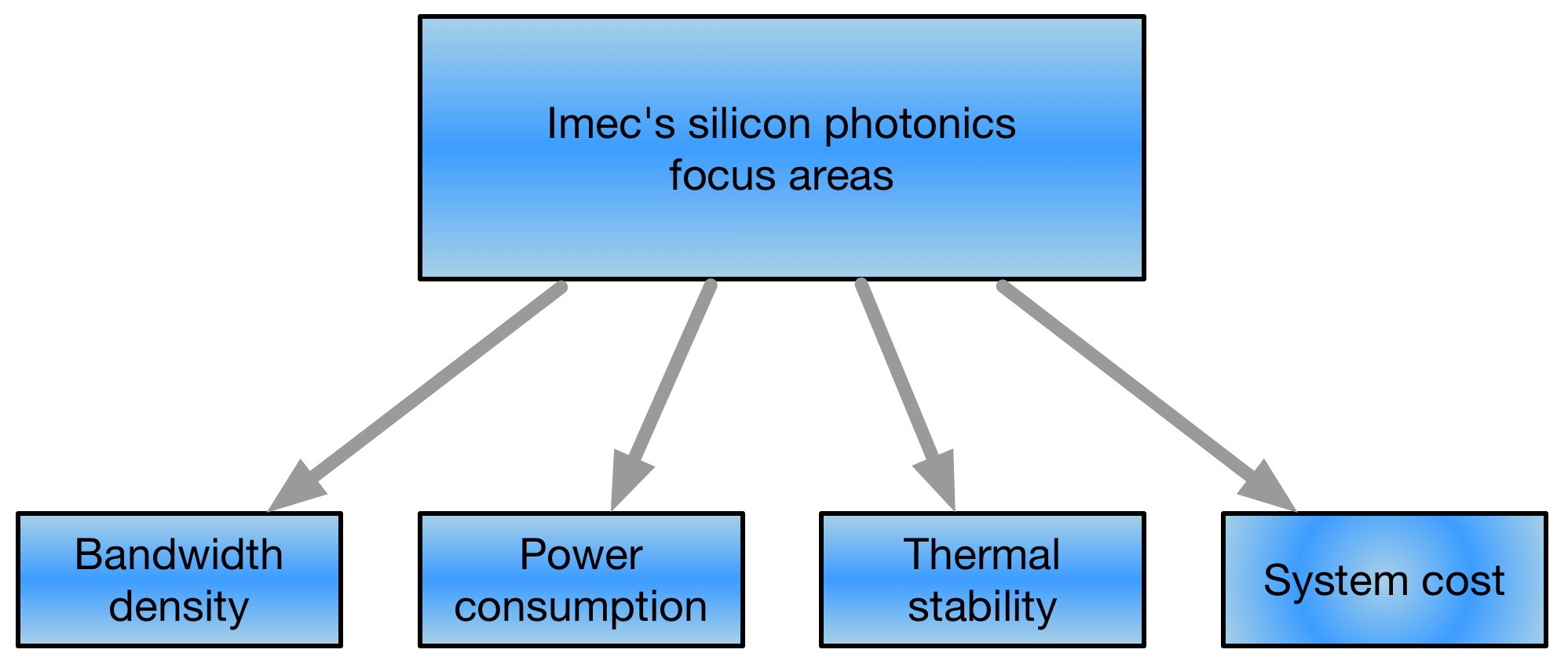
Imec's research concentrates on board-to-board and chip-to-chip interconnect. The optical interconnect work includes increasing interface bandwidth density, reducing power consumption, and achieving thermal stability and system-cost reduction.
The research centre has demonstrated high-bandwidth interfaces as part of work with Chiral Photonics that makes multi-core fibre. Imec has developed a 2D ring of grating couplers that allow coupling between the silicon photonics chip and Chiral's 61-core fibre. "A grating coupler is a sub-wavelength structure that diffracts the light from a waveguide in a vertical direction towards the fibre above the chip," says Absil. This contrasts to traditional edge coupling to a device, achieved by dicing or cleaving a facet on the waveguide, he says.
Another research focus is how to reduce device power consumption and achieve thermal stability. One silicon photonics component that dictates the overall power consumption is the modulator, says Absil. "The Mach-Zehnder modulator is known to consume significant amounts of power for chip-to-chip distances," he says. "The alternative is to use resonating-based modulators but these have to be thermally controlled, and that has an associated power consumption."
Imec is looking at ways to reduce the thermal control needed and is investigating the addition of materials to silicon to create resonator modulators that do away with the need for heating.
The system-cost reduction work looks at packaging. "Eventually, we want to get the optical transceiver inside a host IC," says Absil. "That package has to enable an optical pass-through, whether it is fibre or an optically-transparent package." Such a requirement differs from established CMOS packaging technology. "The programme is also looking to explore new types of packaging for enabling this optical pass-through," he says.
Absil says certain programme elements are two years away from being completed. "In the programme, we have topics that are closer to being adopted and some that are further away, maybe even to 2020."
Multi-project wafer service
Imec is part of the a consortium of EC research institutes that provide low-cost access to companies that don't have the means to manufacture their own silicon photonics designs. Known as Essential, the EC's Seventh Framework (FP7) programme is an extension of the ePIXfab silicon photonics multi-project wafer initiative. "Imec is offering one flavour of the technology, Leti is also offering a flavour, and then there is IHP and VTT," says Absil. Once the Essential FP7 project is completed, the service will be continued by the Europractice IC service.
Has imec seen any growth now that the funding for OpSIS, the multi-project wafer provider, has come to an end? "We see decent contributions but I wouldn't say it is exponential growth," says Absil, who notes that the A*STAR Institute of Microelectronics in Singapore that OpSIS used continues to offer a multi-project wafer service.
Status of silicon photonics
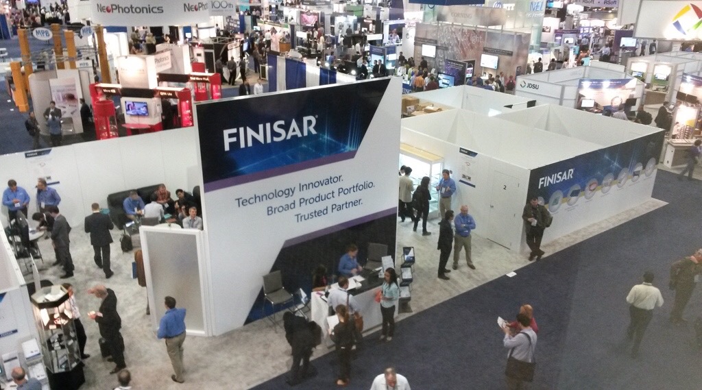
Despite announcements from Acacia and Intel, and Finisar revealing at ECOC '14 that it is now active in silicon photonics, 2014 has been a quiet year for the technology.
"Right now it is a bit quiet because companies are investing in development," says Absil. "There is not so much incentive to publish this work." Another factor he cites for the limited news is that there are vertically-integrated vendors that are putting the technology in their servers rather than selling silicon-photonics products directly.
"This is only first generation," says Absil. "As it picks up, there will be more incentive to work on a second generation of silicon photonics which will depart from what we know from the early work published by Intel and Luxtera."
The opportunities this next-generation technology will offer are 'quite exciting', says Absil.
STMicro chooses PSM4 for first silicon photonics product
- Lowers the manufacturing cost of optical modules
- Improves link speeds
- Reduces power consumption
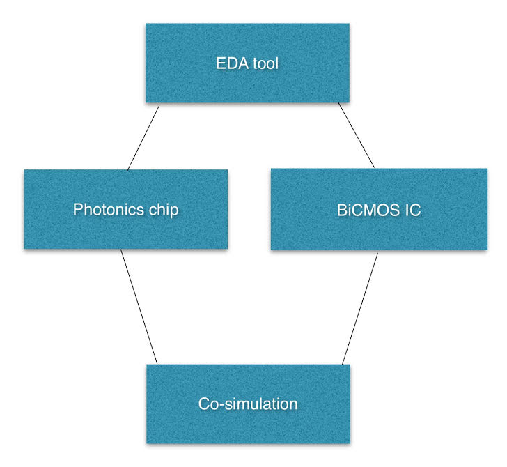 STMicro's in-house silicon photonics EDA. "We will develop the EDA tools to the level needed for the next generation products," says Flavio Benetti.
Silicon photonics book scheduled for early 2016
The work will provide an assessment of silicon photonics and its market impact over the next decade. The title will explore key trends and challenges facing the telecom and datacom industries, provide a history of silicon photonics, and detail its importance. The title will also pinpoint those applications that will benefit most from the technology.