
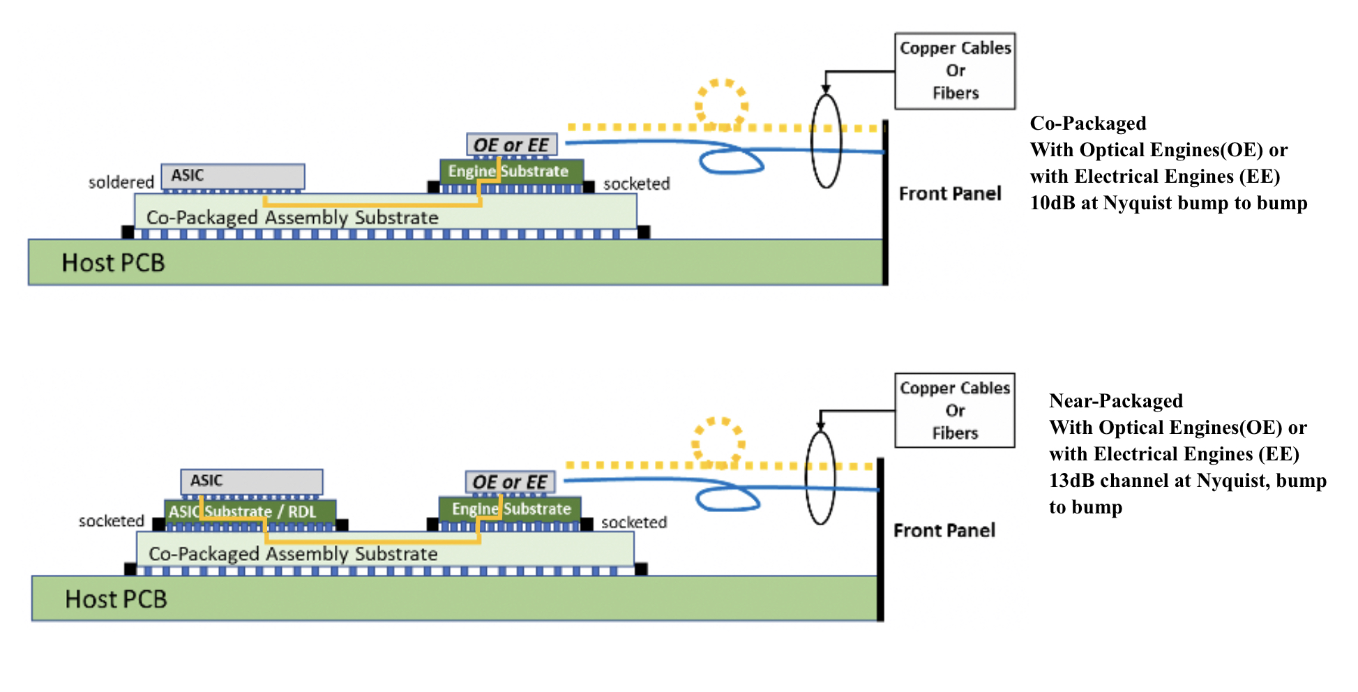
The various paths to co-packaged optics

Near package optics has emerged as companies have encountered the complexities of co-packaged optics. It should not be viewed as an alternative to co-packaged optics but rather a pragmatic approach for its implementation.
Co-packaged optics will be one of several hot topics at the upcoming OFC show in March.
Placing optics next to silicon is seen as the only way to meet the future input-output (I/O) requirements of ICs such as Ethernet switches and high-end processors.
For now, pluggable optics do the job of routing traffic between Ethernet switch chips in the data centre. The pluggable modules sit on the switch platform’s front panel at the edge of the printed circuit board (PCB) hosting the switch chip.
But with switch silicon capacity doubling every two years, engineers are being challenged to get data into and out of the chip while ensuring power consumption does not rise.
One way to boost I/O and reduce power is to use on-board optics, bringing the optics onto the PCB nearer the switch chip to shorten the electrical traces linking the two.
The Consortium of On-Board Optics (COBO), set up in 2015, has developed specifications to ensure interoperability between on-board optics products from different vendors.
However, the industry has favoured a shorter still link distance, coupling the optics and ASIC in one package. Such co-packaging is tricky which explains why yet another approach has emerged: near package optics.
I/O bottleneck
“Everyone is looking for tighter and tighter integration between a switch ASIC, or ‘XPU’ chip, and the optics,” says Brad Booth, president at COBO and principal engineer, Azure hardware architecture at Microsoft. XPU is the generic term for an IC such as a CPU, a graphics processing unit (GPU) or even a data processing unit (DPU).
What kick-started interest in co-packaged optics was the desire to reduce power consumption and cost, says Booth. These remain important considerations but the biggest concern is getting sufficient bandwidth on and off these chips.
“The volume of high-speed signalling is constrained by the beachfront available to us,” he says.
Booth cites the example of a 16-lane PCI Express bus that requires 64 electrical traces for data alone, not including the power and ground signalling. “I can do that with two fibres,” says Booth.

Near package optics
With co-packaged optics, the switch chip is typically surrounded by 16 optical modules, all placed on an organic substrate (see diagram below).
“Another name for it is a multi-chip module,” says Nhat Nguyen, senior director, solutions architecture at optical I/O specialist, Ayar Labs.
A 25.6-terabit Ethernet switch chip requires 16, 1.6 terabits-per-second (1.6Tbps) optical modules while upcoming 51.2-terabit switch chips will use 3.2Tbps modules.
“The issue is that the multi-chip module can only be so large,” says Nguyen. “It is challenging with today’s technology to surround the 51.2-terabit ASIC with 16 optical modules.”
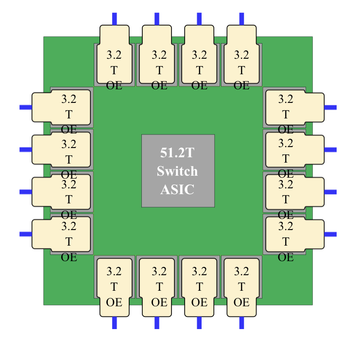
Near package optics tackles this by using a high-performance PCB substrate – an interposer – that sits on the host board, in contrast to co-packaged optics where the modules surround the chip on a multi-chip module substrate.
The near package optics’ interposer is more spacious, making the signal routing between the chip and optical modules easier while still meeting signal integrity requirements. Using the interposer means the whole PCB doesn’t need upgrading which would be extremely costly.
Some co-packaged optics design will use components from multiple suppliers. One concern is how to service a failed optical engine when testing the design before deployment. “That is one reason why a connector-based solution is being proposed,” says Booth. “And that also impacts the size of the substrate.”

A larger substrate is also needed to support both electrical and optical interfaces from the switch chip.
Platforms will not become all-optical immediately and direct-attached copper cabling will continue to be used in the data centre. However, the issue with electrical signalling, as mentioned, is it needs more space than fibre.
“We are in a transitional phase: we are not 100 per cent optics, we are not 100 per cent electrical anymore,” says Booth. “How do you make that transition and still build these systems?”
Perspectives
Ayar Labs views near package optics as akin to COBO. “It’s an attempt to bring COBO much closer to the ASIC,” says Hugo Saleh, senior vice president of commercial operations and managing director of Ayar Labs U.K.
However, COBO’s president, Booth, stresses that near package optics is different from COBO’s on-board optics work.
“The big difference is that COBO uses a PCB motherboard to do the connection whereas near package optics uses a substrate,” he says. “It is closer than where COBO can go.”
It means that with near package optics, there is no high-speed data bandwidth going through the PCB.
Booth says near package optics came about once it became obvious that the latest 51.2-terabit designs – the silicon, optics and the interfaces between them – cannot fit on even the largest organic substrates.
“It was beyond the current manufacturing capabilities,” says Booth. “That was the feedback that came back to Microsoft and Facebook (Meta) as part of our Joint Development Foundation.”
Near package optics is thus a pragmatic solution to an engineering challenge, says Booth. The larger substrate remains a form of co-packaging but it has been given a distinct name to highlight that it is different to the early-version approach.
Nathan Tracy, TE Connectivity and the OIF’s vice president of marketing, admits he is frustrated that the industry is using two terms since co-packaged optics and near package optics achieve the same thing. “It’s just a slight difference in implementation,” says Tracy.
The OIF is an industry forum studying the applications and technology issues of co-packaging and this month published its framework Implementation Agreement (IA) document.
COBO is another organisation working on specifications for co-packaged optics, focussing on connectivity issues.
Technical differences
Ayar Labs highlights the power penalty using near package optics due to its use of longer channel lengths.
For near package optics, lengths between the ASIC and optics can be up to 150mm with the channel loss constrained to 13dB. This is why the OIF is developing the XSR+ electrical interface, to expand the XSR’s reach for near package optics.
In contrast, co-packaged optics confines the modules and host ASIC to 50mm of each other. “The channel loss here is limited to 10dB,” says Nguyen. Co-packaged optics has a lower power consumption because of the shorter spans and 3dB saving.
Ayar Labs highlights its optical engine technology, the TeraPHY chiplet that combines silicon photonics and electronics in one die. The optical module surrounding the ASIC in a co-packaged design typically comprises three chips: the DSP, electrical interface and photonics.
“We can place the chiplet very close to the ASIC,” says Nguyen. The distance between the ASIC and the chiplet can be as close as 3-5mm. Whether on the same interposer Ayar Labs refers to such a design using athird term: in-package optics.
Ayar Labs says its chiplet can also be used for optical modules as part of a co-packaged design.
The very short distances using the chiplet result in a power efficiency of 5pJ/bit whereas that of an optical module is 15pJ/bit. Using TeraPHY for an optical module co-packaged design, the power efficiency is some 7.5pJ/bit, half that of a 3-chip module.
A 3-5mm distance also reduces the latency while the bandwidth density of the chiplet, measured in Gigabit/s/mm, is higher than the optical module.
Co-existence
Booth refers to near package optics as ‘CPO Gen-1’, the first generation of co-packaged optics.
“In essence, you have got to use technologies you have in hand to be able to build something,” says Booth. “Especially in the timeline that we want to demonstrate the technology.”
Is Microsoft backing near package optics?

“We are definitely saying yes if this is what it takes to get the first level of specifications developed,” says Booth.
But that does not mean the first products will be exclusively near package optics.
“Both will be available and around the same time,” says Booth. “There will be near packaged optics solutions that will be multi-vendor and there will be more vertically-integrated designs; like Broadcom, Intel and others can do.”
From an end-user perspective, a multi-vendor capability is desirable, says Booth.
Ayar Labs’ Saleh sees two developing paths.
The first is optical I/O to connect chips in a mesh or as part of memory semantic designs used for high-performance computing and machine learning. Here, the highest bandwidth and lowest power are key design goals.
Ayar Labs has just announced a strategic partnership with high performance computing leader, HPE, to design future silicon photonics solutions for HPE’s Slingshot interconnect that is used for upcoming Exascale supercomputers and also in the data centre.
The second path concerns Ethernet switch chips and here Saleh expects both solutions to co-exist: near package optics will be an interim solution with co-packaged optics dominating longer term. “This will move more slowly as there needs to be interoperability and a wide set of suppliers,” says Saleh.
Booth expects continual design improvements to co-packaged optics. Further out, 2.5D and 3D chip packaging techniques, where silicon is stacked vertically, to be used as part of co-packaged optics designs, he says.

Huawei sets transmission record with new modulator

Coherent discourse: Part 1
A paper from Huawei and Sun Yat-Sen University in the January issue of the Optica journal describes a thin-film lithium niobate modulator. The modulator enabled a world-record coherent optical transmission, sending nearly 2 terabits of data over a single wavelength.
Much of the industry’s focus in recent years has been to fit coherent optical technology within a pluggable module.
Such pluggables allow 400-gigabit coherent interfaces to be added to IP routers and switches, serving the needs of the data centre operators and telecom operators.
But research labs of the leading optical transport vendors continue to advance high-end coherent systems beyond 800-gigabit-per-wavelength transmissions.
Optical transport systems from Ciena, Infinera and Huawei can send 800-gigabit wavelengths using a symbol rate of 96-100 gigabaud (GBd).
Acacia Communications, part of Cisco, detailed late last year the first 1.2-terabit single-wavelength coherent pluggable transceiver that will operate at 140GBd, twice the symbol rate of 400-gigabit modules such as 400ZR.
Now Huawei has demonstrated in the lab a thin-film lithium niobate modulator that supports a symbol rate of 220GBd and beyond.
Maxim Kuschnerov, director of the optical and quantum communications laboratory at Huawei, says the modulator has a 110GHz 3dB bandwidth but that it can be operated at higher frequencies, suggesting a symbol rate as high as 240GBd.
Thin-film lithium niobate modulator
Huawei says research is taking place into new materials besides the established materials of indium phosphide and silicon photonics. “It is a very exciting topic lately,” says Kuschnerov.
He views the demonstrated thin-film lithium niobate optical modulator as disruptive: “It can cover up several deficiencies of today’s modulators.”
Besides the substantial increase in bandwidth – the objective of any new coherent technology – the modulator has performance metrics that benefit the coherent system such as a low driving voltage and low insertion loss.
A driving voltage of a modulator is a key performance parameter. For the modulator, it is sub-1V.
The signal driving the modulator comes from a digital-to-analogue (D/A) converter, part of the coherent digital signal processor (DSP). The D/A output is fed into a modulator driver. “That [driver] requires power, footprint, and increases the complexity of integrating the [modem’s] modules tighter,” says Kuschnerov.
The modulator’s sub-1V drive voltage is sufficiently small that the DSP’s CMOS-based D/A can drive it directly, removing the modulator driver circuit that also has bandwidth performance limitations. The modulator thus reduces the transmitter’s overall cost.
The low-loss modulator also improves the overall optical link budget. And for certain applications, it could even make the difference as to whether optical amplification is needed.
“The modulator checks the box of very high bandwidth,” says Kuschnerov. “And it helps by not having to add a semiconductor optical amplifier for some applications, nor needing a driver amplifier.”
One issue with the thin-film modulator is its relative size. While not large – it has a length of 23.5mm – it is larger than indium phosphide and silicon photonics modulators.
1.96-terabit wavelength
Huawei’s lab set-up used a transmit coherent DSP with D/As operating at 130 Giga-samples-per-second (GS/s) to drive the modulator. The modulation used was a 400-quadrature amplitude modulation (400-QAM) constellation coupled with probabilistic constellation shaping.
A 10 per cent forward error correction scheme was used such that, overall, 1.96-terabits per second of data was sent using a single wavelength.
The D/A converter was implemented in silicon germanium using high-end lab equipment to generate the signal at 130GS/s.
“This experiment shows how much we still need to go,” says Kuschnerov. “What we have done at 130GBd shows there is a clear limitation with the D/A [compared to the 220GBd modulator].”
Baud-rate benefits
Increasing the baud rate of systems is not the only approach but is the favoured implementation choice.
What customers want is more capacity and reducing the cost per bit for the same power consumption. Increasing the baud rate decreases the cost and power consumption of the optical transceiver.
By doubling the baud rate, an optical transceiver delivers twice the capacity for a given modulation scheme. The cost per bit of the transceiver decreases as does the power consumed per bit. Instead of two transceivers and two sets of components, one transceiver and one set are used instead.
But doubling the baud rate doesn’t improve the optical system’s spectral efficiency since doubling the baud rate doubles the channel width. That said, algorithmic enhancements are added to each new generation of coherent modem but technically, the spectral efficiency practically no longer improves.
Huawei acknowledges that while the modulator promises many benefits, all the coherent modem’s components – the coherent ASIC, the D/A and analogue-to-digital (D/A) converters, the optics, and the analogue circuitry – must equally scale. This represents a significant challenge.
Kuschnerov says optical research is finding disruptive answers but scaling performance, especially on the electrical side, remains a critical issue. “How do you increase the D/A sampling rates to match these kinds of modulator technologies?” he says. “It is not straightforward.”
The same is true for the other electrical components: the driver technologies and the trans-impedance amplifier circuits at the receiver.
Another issue is combining the electrical and optical components into a working system. Doubling the signalling of today’s optical systems is a huge radio frequency design and packaging challenge.
But the industry consensus is that with newer CMOS processes and development in components and materials, doubling the symbol rate again to 240GB will be possible.
But companies don’t know – at least they are not saying – what the upper symbol rate limit will be. The consensus is that increasing the baud rate will end. Then, other approaches will be pursued.
Kuschnerov notes that if a 1.6-terabit transceiver could be implemented using a single wavelength or with eight 200Gbps ones with the same spectral performance, cost, footprint and power consumption, end users wouldn’t care which of the two were used.
However, does optics enable such greater parallelism?
Kuschnerov says that while decades of investment has gone into silicon photonics, it is still not there yet.
“It doesn’t have the cost-effectiveness at 16, 32 or 64 lanes because the yield goes down significantly,” he says. “We as an industry can’t do it yet.”
He is confident that, soon enough, the industry will figure out how to scale the optics: “With each generation, we are getting better at it.”
Coherent engineers will then have more design options to meet the system objectives.
And just like with microprocessors, it will no longer be upping the clock frequency but rather adopting parallel processing i.e. multiple cores. Except, in this case, it will be parallel coherent optics.

Intel sets a course for scalable optical input-output

- Intel is working with several universities to create building-block circuits to address its optical input-output (I/O) needs for the next decade-plus.
- By 2024 the company wants to demonstrate the technologies achieving 4 terabits-per-second (Tbps) over a fibre at 0.25 picojoules-per-bit (pJ/b).
Intel has teamed up with seven universities to address the optical I/0 needs for several generations of upcoming products.
The initiative, dubbed the Intel Research Center for Integrated Photonics for Data Centre Interconnects, began six months ago and is a three-year project.
No new location is involved, rather the research centre is virtual with Intel funding the research. By setting up the centre, Intel’s goal is to foster collaboration between the research groups.
Motivation
James Jaussi, senior principal engineer and director of the PHY Research Lab in Intel Labs, (pictured) heads a research team that focuses on chip-to-chip communication involving electrical and optical interfaces.
“My team is primarily focussed on optical communications, taking that technology and bringing it close to high-value silicon,” says Jaussi.
Much of Jaussi’s 20 years at Intel has focussed on electrical I/O. During that time, the end of electrical interfaces has repeatedly been predicted. But copper’s demise has proved overly pessimistic, he says, given the advances made in packaging and printed circuit board (PCB) materials.
But now the limits of copper’s bandwidth and reach are evident and Intel’s research arm wants to ensure that when the transition to optical occurs, the technology has longevity.
“This initiative intends to prolong the [optical I/O] technology so that it has multiple generations of scalability,” says Jaussi. And by a generation, Jaussi means the 3-4 years it takes typically to double the bandwidth of an I/O specification.
Co-packaged optics and optical I/O
Jaussi distinguishes between co-packaged optics and optical I/O.
He describes co-packaged optics as surrounding a switch chip with optics. Given the importance of switch chips in the data centre, it is key to maintain compatibility with specifications, primarily Ethernet.
But that impacts the power consumption of co-packaged optics. “The power envelope you are going to target for co-packaged optics is not necessarily going to meet the needs of what we refer to as optical I/O,” says Jaussi.
Optical I/O involves bringing the optics closer to ICs such as CPUs and graphics processor units (GPUs). Here, the optical I/O need not be aligned with standards.
The aim is to take the core I/O off a CPU or GPU and replace it with optical I/O, says Jaussi.
With optical I/O, non-return-to-zero (NRZ) signalling can be used rather than 4-level pulse amplitude modulation (PAM-4). The data rates are slower using NRZ but multiple optical wavelengths can be used in parallel. “You can power-optimise more efficiently,” says Jaussi.
Ultimately, co-packaged optics and optical I/O will become “stitched together” in some way, he says.
Research directions
One of the research projects involves the work of Professor John Bowers and his team at the University of California, Santa Barbara, on the heterogeneous integration of next-generation lasers based on quantum-dot technology.
Intel’s silicon photonics transceiver products use hybrid silicon quantum well lasers from an earlier collaboration with Professor Bowers.
The research centre work is to enable scalability by using multi-wavelength designs as well as enhancing the laser’s temperature performance to above 100oC. This greater resilience to temperature helps the laser’s integration alongside high-performance silicon.
Another project, that of Professor Arka Majumdar at the University of Washington, is to develop non-volatile reconfigurable optical switching using silicon photonics.
“We view this as a core building block, a capability,” says Jaussi. The switching element will have a low optical loss and will require liitle energy for its control.
The switch being developed is not meant to be a system but an elemental building block, analogous to a transistor, Intel says, with the research exploring the materials needed to make such a device.
The work of Professor S.J. Ben Yoo at University of California, Davis, is another of the projects.
His team is developing a silicon photonics-based modulator and a photodetector technology to enable 40-terabit transceivers at 150fJ/bit and achieving 16Tb/s/mm I/O density.
“The intent is to show over a few fibres a massive amount of bandwidth,” says Jaussi.
Goals
Intel says each research group has its own research targets that will be tracked.
All the device developments will be needed to enable the building of something far more sophisticated in future, says Jaussi.
At Intel Labs’ day last year, the company spoke about achieving 1Tbps of I/O at 1pJ/s. The research centre’s goals are more ambitious: 4Tbps over a fibre at 0.25pJ/b in the coming three years.
There will be prototype demonstrations showing data transmissions over a fibre or even several fibres. “This will allow us to make that scalable not just for one but two, four, 10, 20, 100 fibres,” he says. “That is where that parallel scalability will come from.”
Intel says it will be years before this technology is used for products but the research goals are aggressive and will set the company’s optical I/O goals.

Marvell’s latest acquisition: switch-chip firm Innovium

- Innovium will be Marvell’s fifth acquisition in four years
Marvell is buying switch-chip maker, Innovium, for $1.1 billion to bolster its revenues from the lucrative data centre market.
The combination of Innovium with Inphi, Marvell’s most recent $10 billion acquisition, will enable the company to co-package optics alongside the high-bandwidth, low-latency switch chips.
Marvell returns to the market to gain a scalable, low-latency architecture
“Inphi has quite a bit of experience shipping silicon photonics with the ColorZ and ColorZ II [modules],” says Nariman Yousefi, executive vice president, automotive, coherent DSP and switch group at Marvell. “And we have programmes inside the company to do co-packaged optics as well.”
Innovium
Innovium’s Teralynx family addresses the needs of large-scale data centres and will complement Marvell’s Prestera switch-chip portfolio that addresses enterprise and carrier applications.
Formed in 2014, Innovium is a private company with a staff of 230, 185 of which are engaged in R&D. The company has also raised a total of $400 million in funding.
Innovium is already shipping its 12.8-terabit Teralynx 7 to a leading cloud provider and expects revenues of $150 million in 2022. And earlier this year, it announced it shipped over 1 million 400-gigabit switch-silicon ports in 2020.
“The top cloud players are the ones that drive most of the revenues,” says Yousefi. “But there is a long list of customers that are engaged with Innovium at different capacities and there are a bunch of Tier-2s [data centre operators].”
Marvell gained the Xpliant programmable switch-chip architecture for the data centre when it acquired Cavium Networks in 2018, says Devan Adams, principal analyst at LightCounting.
But soon after the acquisition, the Xpliant switch chip line was discontinued as Marvell decided to concentrate on expanding its Prestera chip family.
Now Marvell has returned to the market to gain a scalable, low-latency architecture that addresses the needs of the mega data centre players.
“When you think of the overall data centre market and how it is booming, Innovium makes Marvell’s solutions more attractive to the key cloud customers by helping them expand their switch-chip offerings,” says Adams.

Marvell says it was impressed with the Innovium design team and with the Teralynx architecture when assessing the company as a potential buy. “We also liked the fact that customers have validated the architecture and that it is shipping and in live networks,” says Yousefi.
Broadcom dominates the switch-chip market. According to the market research company, 650 Group, Broadcom had 72 per cent of the 50-gigabit serialiser-deserialiser (serdes) cloud-based switch market in the first quarter, 2021, while Innovium had 27 per cent.
The cloud players want a choice of suppliers, not just for procurement reasons but to ensure sufficiently strong suppliers that can address their needs.
This latest acquisition, expected to close before the year-end, will be Marvell’s fifth acquisition in four years.
Marvell acquired Inphi earlier this year and two custom ASIC companies in 2019: Avera Semiconductor, originally the ASIC group of IBM Microelectronics, and Aquantia that has multi-gigabit PHY expertise. A year before that, Marvell acquired Cavium, as mentioned.
Marvell will use its sales force to promote Innovium’s products to a larger customer base including customers using its Prestera switch chips.
Adams also notes that Marvell has a broad supply chain and a strategic relationship with leading foundry TSMC that will benefit Innovium in the making of its chips, especially when semiconductors are currently in short supply.
Switch chip styles
There are two types of Ethernet switch chips. For the mega data centres, what is important is capacity and the chip’s throughput per Watt (gigabit-per-second/ Watt). Cloud players need to move traffic efficiently in the data centre and with a low latency. Such chips have a streamlined packet-processing capability. Examples include Broadcom’s Tomahawk and Innovium’s Teralynx lines.
In contrast, enterprises need to support various networking protocols and that requires a broad feature set and packet-processing capability. Marvell’s Prestera and Broadcom’s Trident portfolios fall into this category.
“It is hard to design one device that addresses both,” says Yousefi. “That is why there are two different architectures, design teams, databases and chips.”
Marvell highlights Innovium’s Teralynx portfolio’s low power and low latency. “Even though the application for these devices is supposed to be streamlined, Innovium has managed to put in programmability features that makes the architecture more flexible,” says Yousefi. “These are important differentiators.”
Innovium’s Teralynx 8 family includes a 7nm CMOS, 25.6-terabit chip with 112 gigabit-per-second (Gbps) serialisers-deserialisers (serdes). “The Teralynx 8 switch chip is in the bring-up phase with customers; it is not shipping in volume yet,” says Yousefi.
A future Teralynx 9 has also been mentioned.
Yousefi confirms there will be a next-generation 51.2-terabit switch chip and devices beyond that; what the next device will be called is to be determined.
The Marvell acquisition will also combine the serdes expertise of Inphi and Innovium. “We are going to help, but right now we can’t really do much as two separate companies,” says Yousefi.
Integration
Yousefi is also definitive about Marvell’s co-packaged optics plans but points out that the adoption of the technology will take time for the whole industry.
The integration of the Innovium team within Marvell will be fine-tuned once the two companies formally merge. At a high-level, the Innovium team will continue to focus on what it does best: the high-capacity product line, says Yousefi.
“The real opportunity is how do you leverage the collective teams’ knowledge and efficiencies, share the best practices, help each other out during peak resource crunches, and release products more efficiently,” he says.
More acquisitions
The Innovium deal follows the likes of Intel buying Barefoot Networks and Nvidia buying networking specialist Mellanox which designs its own switch chips.
For Adams, it was those deals that suggested it was only a question of time before someone bid for Innovium.
Adams admits he has no insight into Marvell’s acquisition plans, but he points to how Marvell had its own server CPU chip, the ThunderX3 chip based on ARM cores, which was cancelled last year. Could Marvell decide to re-enter the market via the acquisition route?
Another potential technology Marvell could acquire is programmable logic. FPGAs are used in the data centre as accelerators. Adams also points out that certain switch vendors have added FPGAs to their platforms for niche applications such as high-frequency trading.
As for artificial intelligence (AI) hardware, Marvell has its own IP and has added hardware blocks for AI as part of it Octean 10 design. So perhaps the buying of an AI chip start-up is less likely for now.
Yousefi does not rule out more Marvell acquisitions. “The industry is all about growth and how you can position yourself to do many things,” he says.
But he stresses it will take Marvell time to absorb the latest acquisitions of Inphi and Innovium: “That is just as important as acquiring the right assets.”

Turning to optical I/O to open up computing pinch points

Getting data in and out of chips used for modern computing has become a key challenge for designers.
A chip may talk to a neighbouring device in the same platform or to a chip across the data centre.
The sheer quantity of data and the reaches involved – tens or hundreds of meters – is why the industry is turning to optical for a chip’s input-output (I/O).
It is this technology transition that excites Ayar Labs.
The US start-up showcased its latest TeraPHY optical I/O chiplet operating at 1 terabit-per-second (Tbps) during the OFC virtual conference and exhibition held in June.
Evolutionary and revolutionary change
Ayar Labs says two developments are driving optical I/O.
One is the exponential growth in the capacity of Ethernet switch chips used in the data centre. The emergence of 25.6-terabit and soon 51.2-terabit Ethernet switches continue to drive technologies and standards.
This, says Hugo Saleh, vice president of business development and marketing, and recently appointed as the managing director of Ayar Labs’ new UK subsidiary, is an example of evolutionary change.
But artificial intelligence (AI) and high-performance computing have networking needs independent of the Ethernet specification.
“Ethernet is here to stay,” says Saleh. “But we think there is a new class of communications that is required to drive these advanced applications that need low latency and low power.”
Manufacturing processes
Ayar Labs’ TeraPHY chiplet is manufactured using GlobalFoundries’ 45nm RF Silicon on Insulator (45RFSOI) process. But Ayar Labs is also developing TeraPHY silicon using GlobalFoundries’ emerging 45nm CMOS-silicon photonics CLO process (45CLO).
The 45RFSOI process is being used because Ayar Labs is already supplying TeraPHY devices to customers. “They have been going out quite some time,” says Saleh.
But the start-up’s volume production of its chiplets will use GlobalFoundries’ 45CLO silicon photonics process. Version 1.0 of the process design kit (PDK) is expected in early 2022, leading to qualified TeraPHY parts based on the process.
One notable difference between the two processes is that 45RFSOI uses a vertical grating coupler to connect the fibre to the chiplet which requires active alignment. The 45CLO process uses a v-groove structure such that passive alignment can be used, simplifying and speeding up the fibre attachment.
“With high-volume manufacturing – millions and even tens of millions of parts – things like time-in-factory make a big difference,” says Saleh. Every second spent adds cost such that the faster the processes, the more cost-effective and scalable the manufacturing becomes.
Terabit TeraPHY
The TeraPHY chiplet demonstrated during OFC uses eight optical transceivers. Each transceiver comprises eight wavelength-division multiplexed (WDM) channels, each supporting 16 gigabit-per-second (Gbps) of data. The result is a total optical I/O bandwidth of 1.024Tbps operating in each direction (duplex link).
“The demonstration is at 16Gbps and we are going to be driving up to 25Gbps and 32Gbps next,” says Saleh.
The chiplet’s electrical I/O is slower and wider: 16 interfaces, each with 80, 2Gbps channels implementing Intel’s Advanced Interface Bus (AIB) technology.
Last December, Ayar Labs showcased advanced parts using the CLO process. The design was a direct-drive part – a prototype of a future-generation product, not the one demonstrated for OFC.
“The direct-drive part has a serial analogue interface that could come from the host ASIC directly into the ring resonators and modulate them whereas the part we have today is the productised version of an AIB interface with all the macros and all the bandwidth enabled,” says Saleh.
Ayar Labs also demonstrated its 8-laser light source, dubbed SuperNova, that drives the chiplet’s optics.
The eight distributed feedback (DFB) lasers are mixed using a planar lightwave circuit to produce eight channels, each comprising eight frequencies of light.
Saleh compares the SuperNova to a centralised power supply in a server that power pools of CPUs and memory. “The SuperNova mimics that,” he says. “One SuperNova or a 1 rack-unit box of 16 SuperNovas distributing continuous-wave light just like distributed voltage [in a server].”
The current 64-channel SuperNova powers a single TeraPHY but future versions will be able to supply light to two or more.
Ayar Labs is using Macom as its volume supplier of DFB lasers.
Significance
Ayar Labs believes the 1-terabit chip-to-chip WDM link is an industry first.
The demo also highlights how the company is getting closer to a design that can be run in the field. The silicon was made less than a month before the demonstration and was assembled quickly. “It was not behind glass and was operating at room temperature,” says Saleh. “It’s not a lab setting but a production setting.”
The same applies to the SuperNova. The light source is compliant with the Continuous-Wave Wavelength Division Multiplexing (CW-WDM) Multi-Source Agreement (MSA) Group that released its first specification revision to coincide with OFC. The CW-WDM MSA Group has developed a specification for 8, 16, and 32-wavelength optical sources.
The CW-WDM MSA promoter and observer members include all the key laser makers as well as the leading ASIC vendors. “We hope to establish an ecosystem on the laser side but also on the optics,” says Saleh.
“Fundamentally, there is a change at the physical (PHY) level that is required to open up these bottlenecks,” says Saleh. “The CW-WDM MSA is key to doing that; without the MSA you will not get that standardisation.”
Saleh also points to the TeraPHY’s optical I/O’s low power consumption which for each link equates to 5pJ/bit. This is about a tenth of the power consumed by electrical I/O especially when retimers are used. Equally, the reach is up to 2km not tens of centimetres associated with electrical links.
Chiplet demand
At OFC, Arista Networks outlined how pluggable optics will be able to address 102.4 terabit Ethernet switches while Microsoft said it expects to deploy co-packaged optics by the second half of 2024.
Nvidia also discussed how it clusters its graphics processing units (GPUs) that are used for AI applications. However, when a GPU from one cluster needs to talk to a GPU in another cluster, a performance hit occurs.
Nvidia is looking for the optical industry to develop interfaces that will enable its GPU systems to scale while appearing as one tightly coupled cluster. This will require low latency links. Instead of microseconds and milliseconds depending on the number of hops, optical I/O reduces the latency to tens of nanoseconds.
“We spec our chiplet as sub-5ns plus the time of flight which is about 5ns per meter,” says Saleh. Accordingly, the transit time between two GPUs 1m apart is 15ns.
Ayar Labs says that after many conversations with switch vendors and cloud players, the consensus is that Ethernet switches will have to adopt co-packaged optics. There will be different introductory points for the technology but the industry direction is clear.
“You are going to see co-packaged optics for Ethernet by 2024 but you should see the first AI fabric system with co-packaged I/O in 2022,” says Saleh.
Intel published a paper at OFC involving its Stratix 10 FPGA using five Ayar Labs’ chiplets, each one operating at 1.6 terabits (each optical channel operating at 25Gbps, not 16Gbps). The resulting FPGA has an optical I/O capacity of 8Tbps, the design part of the US DARPA PIPES (Photonics in the Package for Extreme Scalability) project.
“A key point of the paper is that Intel is yielding functional units,” says Saleh. The paper also highlighted the packaging and assembly achievements and the custom cooling used.
Intel Capital is a strategic investor in Ayar Labs, as is GlobalFoundries, Lockheed Martin Ventures, and Applied Materials.

SiDx's use of silicon photonics for blood testing
Part 4: Biosensor start-up, SiDx
A blood sample reveals much about a person’s health. But analysing the sample is complicated given its many constituents.
Identifying a user’s blood type is also non-trivial.
If a patient arriving at hospital needs a blood transfusion, the universal donor blood type, O negative, is administered. That’s because it takes too long – 45 minutes typically – to identify the patient’s blood type. This also explains the huge demand for O negative blood.
Identifying blood type promptly is what start-up SiDx set out to address with a platform based on a silicon photonics sensor. The resulting platform does more than just blood-type identification.
SiDx
The Seattle-based start-up was founded in 2017. By then, SiDx had a decade of research behind it, in silicon-photonics biosensors and the associated biochemistry.
SiDx had also started working with a blood centre in Seattle. Such centres source and sell blood to US hospitals.
“We were looking for an application that justified starting the company,” says Jonas Flueckiger, vice president of engineering at SiDx.
Flueckiger notes that silicon photonics is one of several ways to analyse biological materials. “It has advantages but there are alternatives,” he says. “You have to find an application where the advantages of silicon photonics can shine.”
Marketplace and challenges
Flueckiger splits the biosensor marketplace into three: centralised lab equipment, bedside and portable equipment, and home testing.
For centralised labs, what matters is the scale and the ability to perform parallel testing. Here, trained staff are required for sample preparation and operating the equipment.
The second category, bedside and portable systems, are compact and rugged platforms designed to deliver results quickly; SiDx’s testing system takes 12 minutes. Such platforms are newer and are the focus of SiDx and other silicon photonics biosensor start-ups.
“As for home tests, you don’t need a doctor’s office, you can do it yourself,” says Flueckiger.
But medical diagnostics is a challenging market to enter. “The biggest challenge is that it is very, very hard to bring something new into the medical space,” says Flueckiger.
Hospitals are conservative establishments with rigid protocols that have test systems that doctors trust.
“Even though you show your system will be better, more efficient, faster, and the patient will be better served, it is still very hard to make a case to replace existing technology in a hospital,” says Flueckiger.
A new biosensor system must show it saves money, almost as important as demonstrating improved performance. “If your device is better but it costs more, that is not enough,” says Flueckiger.
Even if a start-up develops a system comparable in price, it must displace existing processes. And that raises a series of questions. Who does the testing? Where do the test results go? And who delivers the news to the patient?
“It is a complex picture and it is not just about technology,” says Flueckiger.

Ring resonators
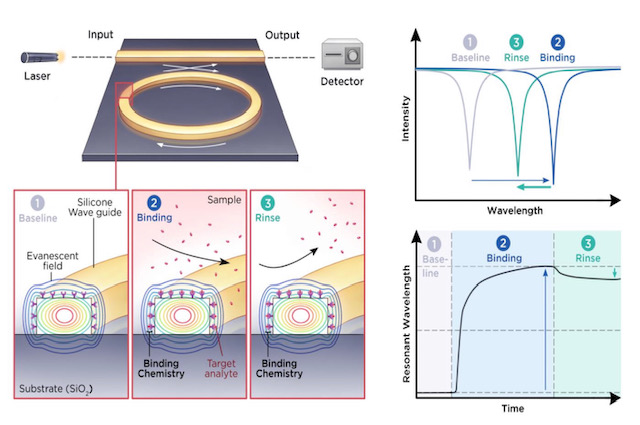
SiDx’s silicon photonics platform measures refractive index changes in light caused by blood sample components attaching to ‘receptors’ placed on the sensor’s surface.
Biochemistry is required to design the receptors for blood analysis and is a core expertise of SiDx.
SiDx uses a laser coupled to a ring resonator. When blood sample constituents attach to the receptors on the ring resonator’s surface, the wavelength at which the sensor resonates changes. This shift in refractive index is used to identify the constituents. (See diagram above.)
A key benefit of the ring resonator approach is its tiny size. Multiple sensors can be integrated into a compact area allowing tests to be performed in parallel. Or as Flueckiger puts it, there is an ability to ask more than one question.
SiDx says it uses ring resonators but it is not detailing its design.
Most emerging integrated-photonics biosensing companies use a laser and ring resonator to read refractive index changes.
One way of get readings is using a tunable laser but alternative designs are possible such as using a fixed laser and tuning the resonator.
That is possible, says Flueckiger, but in a multiplexed design where multiple ring resonators are used, the electrical input-output for all the resonators gets tricky.
“Even for a single test, a single marker, you will have a negative control, a positive control, usually one or two more to make sure you have what you think you have,” says Flueckiger. “With bodily fluids like blood, it is complex and includes stuff that can interfere.”
Silicon photonics also enables label-free detection.
Here, only receptors are used to catch a blood constituent of interest. There is no need for labels with fluorescent attachments designed to link to the constituent.
But labelling improves the probability of identifying what is being looked for. Blood is so complex a sample that doctors may not want label-free testing for just this reason, the risk that another biomarker gives a similar response to what is being sought.
SiDx says sample preparation is key here. Rather than simply squirting the blood sample into the device, additional steps are used such as dilution or separating red blood cells from the serum with testing performed on either. Reagents can also be added to remove all the cells’ membranes.
Such sample preparation steps before label-free testing are important and non-trivial. “Photonics, that is the easy part,” says Flueckiger.
The resulting biosensor comprises optics and biology. Yet it requires a shelf life of 6-12 months. Another reason why medical biosensor design – and the biochemistry in particular – is challenging.
Blood testing and disease screening
Most people understand major blood types such as A, B, AB or O negative, says Flueckiger. But it is more complicated than that in that there are many subgroups. If they are assessed wrongly, it can prove harmful to a patient.
SiDx’s platform can perform blood typing and also Rhesus tests during pregnancy. Rhesus disease is caused by a certain mix of blood types between a pregnant mother and the unborn child.
SiDx sees blood typing as an entry to the market: to prove its technology before branching out. “Once you have blood typing and a sample, you can expand the test portfolio,” says Flueckiger.
The aim is to group tests in an offering that make sense. For example, testing for covid-19 but also testing for the common flu. Or, if a patient tests negative for covid-19, what else could it be? Testing that way and getting an answer avoids the need for a second test.
There are multiple ways to test for covid-19.
A PCR test looks for the DNA of the virus. Analysing a blood sample determines if a body’s immune response has developed antibodies to the virus. If so, it means the person has, or has had, covid-19. SiDx’s biosensor will also be able to test a person’s immune system after a vaccine and determine if a booster jab is needed.
SiDx’s system can detect DNA, but an issue is that DNA needs ‘amplification’; its levels are too small otherwise.
Using integrated photonics coupled with the right capture molecules on the surface allows what is captured to be detected. A DNA molecule is much smaller so other tricks are needed to measure it. As a result, antibodies are more commonly tested for because it is much easier, says Flueckiger.
Prospects
SiDx along with other silicon photonics biosensor companies such as Genalyte, SiPhox, Rockley Photonics and Antelope DX, all received recent funding rounds. SiDx has raised a total of $3 million in funding and $2 million in research funding.
Is this not a vote of confidence in what is a tough market to crack?
There is venture money but it is hard to come by, says Flueckiger. Developing a medical device takes time, a minimum of five years before getting somewhere. If a company starts from scratch, the development time is longer than what venture capitalists are happy with.
Companies pursuing blood testing also can expect greater scrutiny given the story of private company, Theranos, whose claims about developing a breakthrough blood analysis system proved false.
Venture capitalists recognise the potential of benchtop devices but their concern is making money and how quickly a start-up can multiply their investment.
“Unless you can show hockey-stick growth, it’s a tough sell,” says Flueckiger. “These are long-term investments, not like a software company.”
That said, the covid-19 pandemic has helped. People now understand the important role such diagnostic equipment can play. They recognise how long it takes and that if money is thrown at the problem, device development can be accelerated.
Despite the challenges, Flueckiger is upbeat. “We have made lots of progress,” he says. “We have proven to ourselves that our technology works.” SiDx says there are developments that bring its platform closer to market that it cannot disclose at present.
The coronavirus pandemic also provided the company with a motivational boost to launch a product that is far easier to use.
SiDx did consider shifting its focus to address covid-19 testing but the pandemic occurred a year too early. “If it happened now, we would be in a lot better position to turn around very quickly with limited money and have a test ready,” says Flueckiger.
SiDx says that its conversations with investors generate excitement but they want proof of a return.
“You go into this knowing you have a long runway – the next five years will be hard – and then there is the question of whether you will be successful or not,” says Flueckiger.
imec’s research work to advance biosensors

Part 3: Biosensor developments
- Pol Van Dorpe discusses the institute’s use of photonics and silicon to develop new designs for medical diagnostics.
- imec has designed a breathalyser that detects the coronavirus with the accuracy of a polymerase chain reaction (PCR) test, a claimed world first.
Optics and photonics are advancing medical diagnostics in two notable ways.
The technologies are helping to shrink diagnostic systems to create new types of medical devices.
“Going from big lab equipment to something much smaller is a clear trend,” says Pol Van Dorpe, a Fellow at imec, the Belgium R&D nanoelectronics and nanotechnology institute.
Photonics and silicon also benefit central labs by creating more powerful test instruments. More functionality and detectors can be integrated in a given area enabling multiple tests in parallel, a technique dubbed multiplexing.
imec’s biosensor work and espertise
imec began its biosensor research in the 1990s, investigating electrical and surface plasmon-based devices. In more recent years, it has added the development of custom biosensor chips for companies.
As examples, imec worked with Panasonic to develop a chip for PCR, a testing technique now known to the public due to covid-19. The R&D institute also worked with Genalyte, a pioneering silicon photonics medical diagnostics company that uses optical waveguides, ring resonators, and a tunable laser for its multiplexing biosensor product.
imec has also developed in-house expertise across several disciplines needed for biosensor development.
Several groups at imec cover photonics, with Van Dorpe heading the group addressing biophotonics and single-molecule electrical devices.
Another group addresses biochemistry and surface chemistry used to coat and activate a sensor’s surface so that receptors can be attached. Receptors are biochemical materials that enable the sensor to trap and detect materials.
A further team covers microfluidics used to deliver liquid samples to the sensor or to mix solutions precisely.
Semiconductor process steps are used to create high-aspect-ratio structures that implement microfluidic structures. Such structures can also be used to sort cells, known as cytometry.
“There are many sensor types, and each has its own fluidic needs,” says Van Dorpe.
Spin-offs
imec has also spun off several biosensor companies.
One, miDiagnostics, raised $16.5 million in funding in 2020. miDiagnostics has a nanofluidic processor (nFP) that performs diagnostic tests on fluids guided through the system using capillary forces. The liquids can be redirected and can even have their flow reversed.
The nFP is configurable depending on the application. It combines nanofluidic processing and PCR for processing biomarkers: from cells and proteins to nucleic acids and small molecules.
Indigo is another spin-off that is developing a glucose monitoring system. A photonics sensor is embedded under the skin and communicates the user’s blood sugar level to a smartphone.
Market trends
The biosensor market is complex. Many actors – labs, doctors and users – in healthcare must be convinced before adopting a biosensor device. For a device to be successful, it must add value compared to existing equipment. Cost is also key as is the use-case and ease of use.
Portable equipment that delivers results promptly so that medical staff can make quick decisions is one example. Others include identifying if a patient has suffered a heart attack or bacterial infections such as sepsis, or enabling a doctor’s office to determine if a patient has a bacterial or viral infection. But no doctor will have 20 devices in their office, each performing a specific test, he says.
Such biosensor devices could also have played a key role during the current coronavirus pandemic.
“I can tell you we were working with companies and if they were several years ahead in their roadmaps, much of this would have been a lot easier,” says Van Dorpe.
Antigen-based quick tests for covid exist but people don’t trust them completely due to their limited sensitivity. It is also still not known when people become contagious. “If you take a nasal swab but are already recovering then you may not be as contagious,” says Van Dorpe.
imec has developed a coronavirus breathalyser. Blowing into a filter, aerosols and small droplets from a person’s lungs are collected. A 5-minute PCR analysis unit delivers a result, informing the person if their breath is infectious.
The goal is to use such systems at airports and large events, but it doesn’t guarantee that a person won’t get sick. “You could have been infected the previous day,” says Van Dorpe.
In clinical trials with UZ Leuven, the university hospital of Leuven, the system has tested viral RNA in exhaled air with high sensitivity.
“Our chip technology can detect quickly the virus particles with the same accuracy as classical PCR tests,” says Van Dorpe. “We are the first in the world to demonstrate this.”
imec is undertaking more clinical trials while improving the test’s robustness and ease of use. “We are discussing the commercialisation of our technology with different parties,” he says.
Biosensor technologies
imec’s toolbox of technologies include silicon nitride optical waveguides, beam splitters, filters, spectrometers, and in-plane and out-of-plane lenses.
imec can deposit waveguides on CMOS and has exploited the technique with CMOS image sensors that have many detectors. “We can use commercial image-sensor wafers and deposit the waveguide technology and use those pixels as detectors,” says Van Dorpe.
Established diagnostic techniques used in medical labs include ELISA, a reference technique to detect proteins, and PCR that tests for nucleic acid detection (DNA/ RNA).
The importance of both lab techniques will not change anytime soon, says Van Dorpe.
One reason why ELISA and PCR are so established is that they use ‘amplification’ to detect minute amounts of the material being tested for – the analyte – in complex samples.
For amplification, another label is used in addition to the receptors. The analyte is attached to an antibody within the label, and it is this second label that provides greater testing sensitivity. This, however, requires sample preparation by trained staff.
In contrast, newer biosensors technologies such as surface plasmon resonance (SPR) and silicon photonics use a label-free approach that does away with the second analyte-label stage.
But the label-free sensor is less sensitive; the technique measures when something attaches to the receptors but it can’t distinguish what it measures.
Van Dorpe stresses that amplification is chemistry-related and so it can be used with silicon photonics or SPR.
It is the overall diagnostic system that determines sensitivity, the combination of the transduction process and the chemistry, says Van Dorpe.
SPR and silicon photonics
SPR and silicon photonics biosensors work by measuring changes in light caused by passing a sample over the sensor which causes molecules to attach to the surface.
An SPR system comprises a laser, a prism attached to a gold surface, and a detector. Light is shone through the prism and is reflected from the gold layer before being detected. At a certain incident angle, the light causes electron resonance on the gold surface causing the reflected light intensity to dip.
Attaching biochemical receptors to the gold surface tailored to the analyte causes a shift in resonance angle and the angle change is a measure of the analyte’s presence.
In contrast, silicon photonic designs measure refractive index changes in the light caused by analytes attached to receptors on the sensor’s surface. Two sensor designs are used: a laser with either a Mach-Zehnder interferometer (MZI) or a ring resonator.
“Everything that changes the refractive index causes a signal,” says Van Dorpe.
imec’s biosensor developments
imec’s work with Genalyte a decade ago involved a biosensor that used a tunable laser and ring-resonator sensors.
More recently, the R&D institute has developed technologies not reflected in the silicon photonics designs used by biosensor start-ups such as Genalyte, SiDx, Antelope DX and SiPhox.
imec’s biosensor technologies have been developed to be less sensitive to non-specific binding. What is measured is fluorescence that occurs with the binding to the analyte.
“In blood or more complicated samples, there is a lot of stuff [besides what is being tested for],” says Van Dorpe.
One technology imec has developed performs rapid ELISA-style testing without needing the repeated wash stages required with ELISA systems.

ELISA uses an antibody receptor to detect the tested-for material while a second antibody uses an enzyme that produces colour. And it is the colour that is measured. In effect, both antibodies detect the analyte but the second, with its fluorescent label, helps determine how much analyte has bound.
With standard ELISA testing, repeated wash steps are required to remove what has not bound to the receptors and labels. These wash stages lengthen the testing time.
imec’s sensor is sensitive in the region very close to the surface. Measuring the fluorescence near the surface determines its build-up over time (see diagram).
The cleverness of the sensor is that the larger the concentration, the faster the surface fills up, reflected in the rate of change of fluorescence over time.
“You don’t need to wait until everything has stabilised to determine the concentration,” says Van Dorpe. “You can wait, say 2 minutes, measure the slope of the signal and that gives you a direct measure of the concentration.”
The design can be used with blood samples, to measure protein production or proteins that shouldn’t be there.
The sensor allows the real-time measurement of biomarkers, and no wash stages are needed. It also enables a controlled process for the biological production of vaccines or cancer therapy.
The key here is that using waveguides and integrated photonics allows localised sensing.
“Also with waveguide technology, because you route light on a chip, you can address a lot of [sensing] sites at the same time,” says Van Dorpe. “That allows you to measure a lot of spots, what is called multiplexing.”
These are the advantages of integrated photonics: the ability to test in parallel and the precise quantification of concentrations, he says.
imec has developed a second fluorescence technique – called super-critical angled fluorescence – closely related to the first but that does away with the waveguide.
As with the first technique, two antibodies are used, one with a fluorescent label.
By exciting the fluorescent label, light is produced in all directions. If a high-angle beam is used, the light at the surface interface refracts within a critical angle.
A fluorescent molecule close to the surface – less than a wavelength away – emits light into a silicon-oxide material. This helps distinguish molecules far from the surface compared to closer ones.
imec’s compact system filters out fluorescence from labels floating further away while measuring those nearby. This is like what happens with the waveguide of the first technique, where it is routed to the detector. But here the detector is situated underneath to measure the fluorescence. The technique delivers rapid results.
The two imec techniques deliver selective sensing that doesn’t rely on refractive index changes or mass. With the latter techniques, all the signals are picked up: everything that binds, wanted and unwanted materials.
The imec techniques are not perfect. There is some degree of auto-fluorescence but it is low. Also, some antibodies with the label will bind to the surface but that is much smaller than the proteins, says Van Dorpe.
Cytometry
imec is working with Sarcura, a cell therapy firm, on a high-throughput cytometry solution for cell separation. Here photonic integration is used along with a microfluidic solution to measure the cells.
A standard cytometer has a flow of cells and a bank of lasers at multiple wavelengths typically. As the cells pass, they scatter the focused light from the lasers. The scattering is measured while the cells also fluoresce since they are labelled. This allows for cell categorisation.
With cell therapy for cancer treatment, immune cells are grown and need analysing. Another use is identifying tumour cells in the blood.
“There are lots of applications where you want to pick out specific cells, label them, look at their properties and classify,” he says.
Traditional equipment used for these tasks is large and complex, requiring skilled staff.
What silicon photonics and microfluidics allow is the bringing of cells to the channel and, with waveguides, illuminate them and detect them.
The result, says Van Dorpe, is a high-throughput design with many adjacent channels.

Nokia shares its vision for cost-reduced coherent optics

Nokia explains why coherent optics will be key for high-speed short-reach links and shares some of its R&D activities. The latest in a series of articles addressing what next for coherent.
Part 3: Reducing cost, size and power
Coherent optics will play a key role in the network evolution of the telecom and webscale players.
The modules will be used for ever-shorter links to enable future cloud services delivered over 5G and fixed-access networks.
The first uses will be to link data centres and support traffic growth at the network edge.
This will be followed with coherent optics being used within the data centre, once traffic growth requires solutions that 4-level pulse-amplitude modulation (PAM4) direct-detect optics can no longer address.
“If you look at PAM4 up to 100 gigabit for long reach and extended reach optics – distances below 80km – it does not scale to higher data rates,” says Marc Bohn, part of product management for Nokia’s optical subsystem group. ”It only scales if you use 100-gigabit in parallel.”
However, to enable short-reach coherent optics, its cost, size and power consumption will need to be reduced significantly. Semiconductor packaging techniques will need to be embraced as will a new generation of coherent digital signal processors (DSPs).
Capacity growth
The adoption of network-edge and on-premise cloud technologies are fueling capacity growth, says Tod Sizer, smart optical fabric & devices research lab leader at Nokia Bell Labs.
Nokia says capacity growth is at 50 per cent per annum and is even faster within the data centre; for every gigabyte entering a data centre, ten gigabytes are transported within the data centre.
“All of this is driving huge amounts of growth in optical capacity at shorter distances,” says Sizer. “To meet that [demand], we need to have coherent solutions to take over where PAM-4 stops.”
Sizer oversees 130 engineers whose research interests include silicon photonics, coherent components and coherent algorithms.
Applications
As well as data centre interconnect, coherent optics will be used for 5G, access and cable networks; markets also highlighted by Infinera and Acacia Communications.

Nokia says the first driver is data centre interconnect.
The large-scale data centre operators triggered the market for 80-120km coherent pluggables with the 400ZR specification for data centre interconnect.
“Right now, with the different architectures in data centres, these guys are saying 80-120km may be an overshoot, maybe we need something for shorter distances to be more efficient,” says Bohn. “Certainly, coherent can tackle that and that is what we are preparing for because there is no alternative, only coherent can cover that space.”
5G is also driving the need for greater bandwidth.
“Traditionally a whole load of processing has been done at the remote ratio head but increasingly, for cost and performance reasons, people are looking at pulling the processing back into the data centre,” says Sizer.
Another traffic driver is how each cellular antenna has three sectors and can use multiple frequency bands.
“Some research we are looking at requires 400 gigabits and above,” says Sizer. “If you want to do a full [mobile] front haul for a massive MIMO (multiple input, multiple output) array, for example.”
Challenges
Several challenges need to be overcome before coherent modules are used widely for shorter-reach links.
To reduce coherent module cost, the optics and DSP need to be co-packaged, borrowing techniques developed by the chip industry.
“Optical and electrical should be brought close together,” says Bohn. “[They should be] co-designed and co-packaged, and the ideal candidate for that is to combine silicon photonics and the DSP.”
The aim is to turn complex designs into a system-on-chip. “Both [the DSP and silicon photonics] are CMOS and you can apply 2D and 3D [die] stacking multi-chip module techniques,” says Bohn, who contrasts it with the custom and manual manufacturing techniques used today.
The coherent DSP also needs to be much simpler than the high-end DSPs used for long-distance optical transport.
For example, the dispersion compensation, which accounts for a significant portion of the chip’s circuitry, is less demanding for shorter links. The forward-error-correction scheme used can also be relaxed as can the bit precision of the analogue-to-digital and digital-to-analogue converters.
Nokia can co-design the silicon photonics and the DSP following its acquisition of Elenion. Nokia is also exploiting Elenion’s packaging know-how and the partnerships it has developed.
Inside the data centre
Nokia highlights two reasons why coherent will eventually be used within the data centre.
The first is the growth in capacity needed inside the data centre. “For the same reason we believe coherent will be the right solution for data centre interconnect and access, the same argument can be made within the data centre,” says Sizer.
A campus data centre is distributed across several buildings and linking them is driving a need for 400-gigabit lanes or more.
This requires a ZR-like solution but for 2km or so rather than 80km.
“It is one of the solutions certainly but that will be driven an awful lot by whether we can make cost-effective solutions to meet the cost targets of the data centre,” says Sizer. That said, there are other ways this can be addressed such as adding fibre.
“Having parallel systems is another area of ongoing research,” says Sizer. “We may need to have unique solutions if traffic grows faster inside the data centre than outside such as spatial-division multiplexing as well as coherent.”
The use of coherent interfaces for networking inside the data centre will take longer.
Bohn points out that 51.2-terabit and 102.4-terabit switches will continue to be served using direct-detect optics but after that, it is unclear because direct-detect optics tops out at 100-gigabits or perhaps 200-gigabits per lane.
“With coherent, it is much easier to get to higher data rates especially over shorter distances,” says Bohn.
Another development benefitting the use of coherent is the next Ethernet standard after 400 Gigabit Ethernet (GbE).
“My research team is looking at that and, in particular, 1.6 Terabit Ethernet (TbE) which is fairly out in the future,” says Sizer. “It will demand a coherent solution, as I expect 800GbE will as well.”
Work to define the next Ethernet standard is starting now and will only be completed in 2025 at the earliest.

Intel combines optics to its Tofino 2 switch chip
Part 1: Co-packaged Ethernet switch
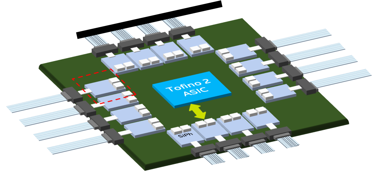
The advent of co-packaged optics has moved a step closer with Intel’s demonstration of a 12.8-terabit Ethernet switch chip with optical input-output (I/O).
The design couples a Barefoot Tofino 2 switch chip to up to 16 optical ‘tiles’ – each tile, a 1.6-terabit silicon photonics die – for a total I/O of 25.6 terabits.
“It’s an easy upgrade to add our next-generation 25.6-terabit [switch chip] which is coming shortly,” says Ed Doe, Intel’s vice president, connectivity group, general manager, Barefoot division.
Intel acquired switch-chip maker, Barefoot, seven months ago after which it started the co-packaging optics project.
Intel also revealed that it is in the process of qualifying four new optical transceivers – a 400Gbase-DR4, a 200-gigabit FR4, a 100-gigabit FR1 and a 100Gbase-LR4 – to add to its portfolio of 100-gigabit PSM4 and CWDM4 modules.
Urgency
Intel had planned to showcase the working co-packaged switch at the OFC conference and exhibition, held last week in San Diego. But after withdrawing from the show due to the Coronavirus outbreak, Intel has continued to demonstrate the working co-packaged switch at its offices in Santa Clara.

“We have some visionaries of the industry coming through and being very excited, making comments like: ‘This is an important milestone’,” says Hong Hou, corporate vice president, general manager, silicon photonics product division at Intel.
“There are a lot of doubts still [about co-packaged optics], in the reliability, the serviceability, time-to-market, and the right intercept point [when it will be needed]: is it 25-, 51- or 102-terabit switch chips?” says Hou. “But no one says this is not going to happen.”
If the timing for co-packaged optics remains uncertain, why the urgency?
“There has been a lot of doubters as to whether it is possible,” says Doe. “We had to show that this was feasible and more than just a demo.”
Intel has also been accumulating IP from its co-packaging work. Topics include the development of a silicon-photonics ring modulator, ensuring optical stability and signal integrity, 3D packaging, and passive optical alignment. Intel has also developed a fault-tolerant design that adds a spare laser to each tile to ensure continued working should the first laser fail.
“We can diagnose which laser is the source of the problem, and we have a redundant laser for each channel,” says Hou. “So instead of 16 lasers we have 32 functional lasers but, at any one time, only half are used.”
Co-packaged optics
Ethernet switches connected in the data centre currently use pluggable optics. The switch chip resides on a printed circuit board (PCB) and is interfaced to the pluggable modules via electrical traces.
But given that the capacity of the Ethernet switch ICs is doubling every two years, the power consumption of the I/O continues to rise yet the power delivered to a data centre is limited. Accordingly, solutions that ensure a doubling of switch speed but do not increase the power consumed are required.
One option is embedded optics such as the COBO initiative. Here, optics are moved from the switch’s faceplate onto the PCB, closer to the switch chip. This shortens the electrical traces while overcoming the capacity limitations of the number of pluggable modules that can be fitted onto the switch’s faceplate. Freeing up the faceplate by removing pluggables also improves airflow to cool the switch.
The second, more ambitious approach is co-packaged optics where optics are combined with the switch ASIC in the one package.
Co-packaged optics can increase the overall I/O on and off the switch chip, something that embedded optics doesn’t address. And placing the optics next to the ASIC, the drive requirements of the high-speed serialiser-deserialisers (serdes) is simplified.
Meanwhile, pluggable optics continue to advance in the form factors used and their speeds as well as developments such as fly-over cables that lower the loss connecting the switch IC to the front-panel pluggables.
In turn, certain hyperscalers are not convinced about co-packaged optics.
Microsoft and Facebook announced last year the formation of the Co-Packaged Optics (CPO) Collaboration to help guide the industry to develop the elements needed for packaging optics. But Google and Alibaba said at OFC that they prefer the flexibility and ease of maintenance of pluggables.
Data centre trends
The data centre is a key market for Intel which sells high-end server microprocessors, switch ICs, FPGAs and optical transceivers.
Large-scale data centres deploy 100,000 servers, 50,000 switches and over one million optical modules. And a million pluggable modules equate to $150M to $250M of potential revenue, says Intel.

“One item that is understated is the [2:1] ratio of servers to switches,” says Doe. “We have seen a trend in recent years where the layers of switching in data centres have increased significantly.”
One reason for more switching layers is that traffic over-subscription is no longer used. With top-of-rack switches, a 3:1 over-subscription was common which limited the switch’s uplink bandwidth needed.
However, the changing nature of the computational workloads now requires that any server can talk to any other server.
“You can’t afford to have any over-subscription at any layer in the network,” says Doe. “As a result, you need to have a lot more bandwidth: an equal amount of downlink bandwidth to uplink bandwidth.”
Another factor that has increased the data centre’s switch layer count is the replacement of chassis switches with disaggregated pizza boxes. Typically, a chassis switch encompasses three layers of switching.
“Disaggregation is a factor but the big one is the 1:1 [uplink-downlink bandwidth] ratio, not just at the top-of-rack switch but all the way through,” says Doe. “They [the hyperscalers] want to have uniform bandwidth throughout the entire data centre.”
Tofino switch IC
Barefoot has two families of Tofino chips. The first-generation Tofino devices have a switching capacity ranging from 1.2 to 6.4 terabits and are implemented using a 16nm CMOS process. The Tofino 2 devices, implemented using a 7nm CMOS IC, range from 4 terabits to 12.8 terabits.
“What we having coming soon is the Tofino next-generation which will go to both 25 terabits and 51 terabits,” says Doe.
Intel is not discussing future products but Doe hints that both switch ICs will be announced jointly rather than the typical two-year delay between successive generations of switch IC. This also explains the urgency of the company’s co-packaging work.
The 12.8-terabit Tofino 2 chip comprises the switch core dies and four electrical I/O tiles that house the device’s serdes.
“The benefit of the tile design is that it allows us to easily swap the tiles for higher-speed serdes – 112 gigabit-per-second (Gbps) – once they become available,” says Doe. And switching the tiles to optical was already envisaged by Barefoot.
Optical tile
Intel’s 1.6-terabit silicon-photonics tile includes two integrated lasers (active and spare), a ring modulator, an integrated modulator driver, and receiver circuitry. “We also have on-chip a v-groove which allows for passive optical alignment,” says Hou.
Each tile implements the equivalent of four 400GBASE-DR4s. The 500m-reach DR4 comprises four 100-gigabit channels, each sent over single-mode fibre.
“This is a standards-based interface,” says Robert Blum, Intel’s director of strategic marketing and business development, as the switch chip must interact with standard-based optics.
The switch chip and the tiles sit on an interposer. Having an interposer will enable different tiles and different system-on-chips to be used in future.
Hou says that having the laser integrated with the tile saves power. This contrasts with designs where the laser is external to the co-packaged design.
The argument for using an external laser is that it is remote from the switch chip which runs hot. But Hou says that the switch chip itself has efficient thermal management which the tile and its laser(s) can exploit. Each tile consumes 35W, he says.
As for laser reliability, Intel points to its optical modules that it has been selling since 2016 when it started selling the PSM4.
Hou claims Intel’s hybrid laser design, where the gain chip is separated from the cavity, is far more reliable than a III-V facet cavity.
“We have shipped over three million 100-gigabit transceivers, primarily the PSM4. The DPM [defects per million] is 28-30, about two orders of magnitude less than our closest competitor,” says Hou. “Eight out of ten times the cause of the failure of a transceiver is the laser, and nine out of ten times, the laser failure is due to a cavity problem.”
The module’s higher reliability reduces the maintenance needed, and enables data centre operators to offer more stringent service-level agreements, says Hou.
Intel says it will adopt wavelength-division multiplexing (WDM) to enable a 3.2-terabit tile which will be needed with the 51.2-terabit Tofino.
Switch platform
Intel’s 2-rack-unit (2RU) switch platform is a hybrid design: interfaced to the Tofino 2 are four tiles as well as fly-over cables to connect the chip to the front-panel pluggables.
“The hyperscalers are most interested in co-packaging but when you talk to enterprise equipment manufacturers, their customers may not have a fabric as complicated as that of the hyperscalers,” says Hou. “Bringing pluggables in there allows for a transition.”
The interposer design uses vertical plug-in connectors enabling a mix of optical and electrical interfaces “It is pretty easy, at the last minute, to [decide to] bring in 10 optical [interfaces] and six fly-over cables [to connect] to the pluggables,” says Hou.
“This is not like on-board optics,” adds Blum. “This [connector arrangement] is part of the multi-chip package, it doesn’t go through the PCB. It allows us to have [OIF-specified] XSR serdes and get the power savings.”
Intel expects its co-packaged design to deliver a 30 per cent power saving as well as a 25 to 30 per cent cost-saving. And now that it has a working platform, Hou expects more engagements with customers that seeking these benefits and its higher-bandwidth density.
“This can stimulate more discussions and drive an ecosystem formation around this technology,” concludes Hou.
See Part 2: Ranovus outlines its co-packaged optics plans.
Nokia buys Elenion for its expertise and partnerships

Nokia will become the latest systems vendor to bolster its silicon photonics expertise with the acquisition of Elenion Technologies.
The deal for Elenion, a privately-held company, is expected to be completed this quarter, subject to regulatory approval. No fee has been disclosed.
“If you look at the vertically-integrated [systems] vendors, they captured the lion’s share of the optical coherent marketplace,” says Kyle Hollasch, director of optical networking product marketing at Nokia. “But the coherent marketplace is shifting to pluggables and it is shifting to more integration; we can’t afford to be left behind.”
Elenion Technologies
Elenion started in mid-2014, with a focus of using silicon as a platform for photonics. “We consider ourselves more of a semiconductor company than an optics company,” says Larry Schwerin, CEO of Elenion.
Elenion makes photonic engines and chipsets and is not an optical module company. “We then use the embedded ecosystem to offer up solutions,” says Schwerin. “That is how we approach the marketplace.”
The company has developed a process design kit (PDK) for photonics and has built a library of circuits that it uses for its designs and custom solutions for customers.
A PDK is a semiconductor industry concept that allows circuit designers to develop complex integrated circuits without worrying about the underlying transistor physics. Adhering to the PDK ensures the circuit design is manufacturable at a chip fabrication plant (fab).
But developing a PDK for optics is tricky. How the PDK is designed and developed must be carefully thought through, as has the manufacturing process, says Elenion.
“We got started on a process and developed a library,” says Larry Schwerin, CEO of Elenion. “And we modelled ourselves on the hyperscale innovation cycle, priding ourselves that we could get down to less than three years for new products to come out.”
The “embedded ecosystem” Elenion refers to involves close relationships with companies such as Jabil to benefit from semiconductor assembly test and packaging techniques. Other partnerships include Molex and webscale player, Alibaba.
Elenion initially focussed on coherent optics, providing its CSTAR coherent device that supports 100- and 200-gigabit transmissions to Jabil for a CFP2-DCO pluggable module. Other customers also use the design, mostly for CFP2-DCO modules.
The company has now developed a third-generation coherent design, dubbed CSTAR ZR, for 400ZR optics. The optical engine can operate up to 600 gigabits-per-second (Gbps), says Elenion.
Elenion’s work with the cloud arm of Alibaba covers 400-gigabit DR4 client-side optics as well as an 800-gigabit design.
Alibaba Cloud has said the joint technology development with Elenion and Hisense Broadband covers all the production stages: the design, packaging and testing of the silicon photonics chip followed by the design, packaging, assembly and testing of the resulting optical module.
Bringing optics in-house
With the acquisition of Elenion, Nokia becomes the latest systems vendors to buy a silicon photonics specialist.
Cisco Systems acquired Lightwire in 2012 that enabled it to launch the CPAK, a 100-gigabit optical module, a year ahead of its rivals. Cisco went on another silicon photonics shopping spree more recently with the acquisition of Luxtera in 2019, and it is the process of acquiring leading merchant coherent player, Acacia Communications.
In 2013 Huawei bought the Belgium silicon photonics start-up, Caliopa, while Mellanox Technologies acquired silicon photonics firm, Kotura, although subsequently, it disbanded its silicon photonics arm.
Ciena bought the silicon-photonics arm of Teraxion in 2016 and, in the same year, Juniper bought silicon photonics start-up, Aurrion Technologies.
Markets
Nokia highlights several markets – 5G, cloud and data centres – where optics is undergoing rapid change and where the system vendor’s designs will benefit from Elenion’s expertise.
“5G is a pretty obvious one; a significant portion of our optical business over the last two years has been mobile front-haul,” says Nokia’s Hollasch. “And that is only going to become more significant with 5G.”
Front-haul is optics-dependent and requires new pluggable form factors supporting lower data rates such as 25Gbps and 100Gbps. “This is the new frontier for coherent,” says Hollasch.
Nokia is not looking to be an optical module provider, at least for now. “That one we are treading cautiously,” says Hollasch. “We, ourselves, are quite a massive customer [of optics] which gives us some built-in scale straight away but our go-to-market [strategy] is still to be determined.”
Not being a module provider, adds Schwerin, means that Nokia doesn’t have to come out with modules to capitalise on what Elenion has been doing.
Nokia says both silicon photonics and indium phosphide will play a role for its coherent optical designs. Nokia also has its own coherent digital signal processors (DSPs).
“There is an increasingly widening application space for silicon photonics,” says Hollasch. “Initially, silicon photonics was looked at for the data centre and then strictly for metro [networks]; I don’t think that is the case anymore.”
Why sell?
Schwerin says the company was pragmatic when it came to being sold. Elenion wasn’t looking to be acquired and the idea of a deal came from Nokia. But once the dialogue started, the deal took shape.
“The industry is in a tumultuous state and from a standpoint of scenario planning, there are multiple dynamics afoot,” says Schwerin.
As the company has grown and started working with larger players including webscales, their requirements have become more demanding.
“As you get more into bigs, they require big,” says Schwerin. “They want supply assurance, and network indemnification clauses come into play.” The need to innovate is also constant and that means continual investment.
“When you weigh it all up, this deal makes sense,” he says.
Schwerin laughs when asked what he plans to do next: “I know what my wife wants me to do.
“I will be going with this organisation for a short while at least,” he says. “You have to make sure things go well in the absorption process involving big companies and little companies.”