
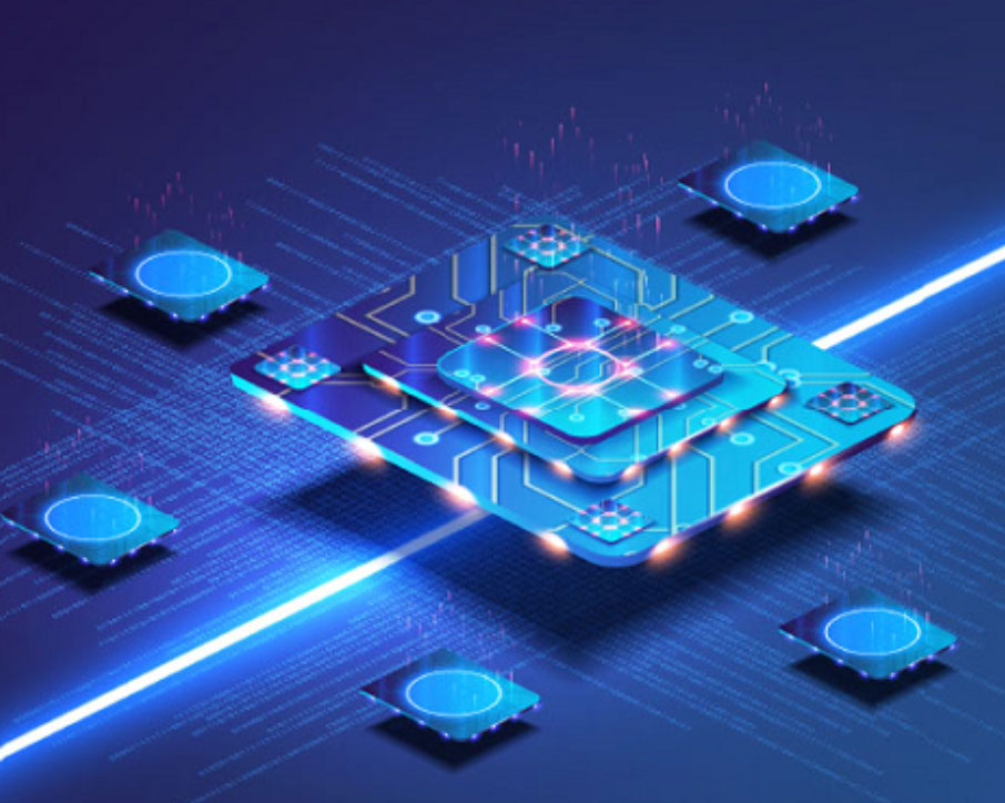
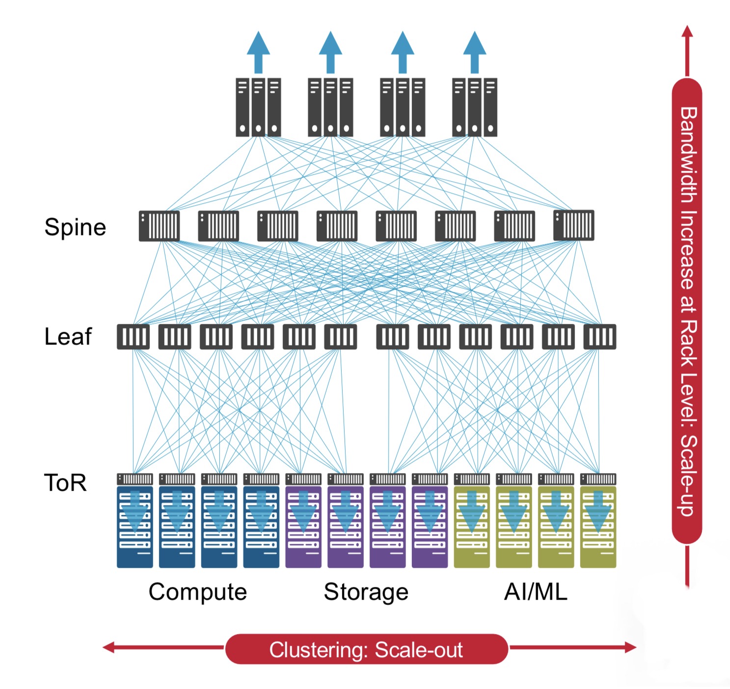
The computing problem of our time: Moving data
- Celestial AI’s Photonic Fabric technology can deliver up to 700 terabits per second of bidirectional bandwidth per chip package.
- The start-up has recently raised $100 million in funding.
The size of AI models that implement machine learning continue to grow staggeringly fast.
Such AI models are used for computer vision, large language models such as ChatGPT, and recommendation systems that rank items such as search results and music playlists.
The workhorse silicon used to build such AI models are graphics processing units (GPUs). GPU processing performance and their memory size may be advancing impressively but AI model growth is far outpacing their processing and input-output [I/O] capabilities.
To tackle large AI model workloads, hundreds and even thousands of GPUs are deployed in parallel for boost overall processing performance and high-performance memory storage capacity.
But it is proving hugely challenging to scale such parallel systems and feed sufficient data to the expensive processing nodes so they can do their work.
Or as David Lazovsky, CEO of start-up Celestial AI puts it, data movement has become the computing problem of our time.
Input-output bottleneck
The data movement challenge and scaling hardware for machine learning has caused certain AI start-ups to refocus, looking beyond AI processor development to how silicon photonics can tackle the input-output [I/O] bottleneck.
Lightelligence is one such start-up; Celestial AI is another.
Founded in 2020, Celestial AI has raised $100 million in its latest round of funding, and $165 million overall.
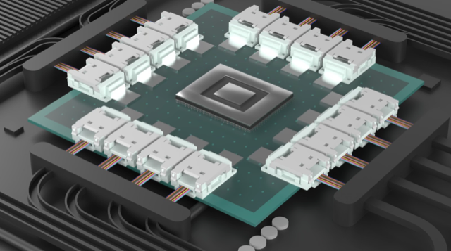
Celestial AI’s products include the Orion AI processor and its Photonic Fabric, an optoelectronic system-in-package comprising a silicon photonics chip and the associated electronics IC.
The Photonic Fabric uses two technological differentiators: a thermally stable optical modulator, and an electrical IC implemented in advanced CMOS.

Thermally stable modulation
Many companies use a ring resonator modulator for their co-packaged optics designs, says Lazovsky. Ring resonator modulators are tiny but sensitive to heat, so they must be temperature-controlled to work optimally.
“The challenge of rings is that they are thermally stable to about one degree Celsius,” says Lazovsky.
Celestial AI uses silicon photonics as an interposer such that it sits under the ASIC, a large chip operating at high temperatures.
“Using silicon photonics to deliver optical bandwidth to a GPU that’s running at 500-600 Watts, that’s just not going to work for a ring,” says Lazovsky, adding that even integrating silicon photonics into memory chips that consume 30W will not work.
Celestial AI uses a 60x more thermally stable modulator than a ring modulator.
The start-up uses continuous wave distributed feedback laser (DFB) lasers as the light source, the same lasers used for 400-gigabit DR4 and FR4 pluggable transceivers, and sets their wavelength to the high end of the operating window.
The result is a 60-degree operating window where the silicon photonics circuits can operate. “We can also add closed-loop control if necessary,” says Lazovsky.
Celestial AI is not revealing the details of its technology, but the laser source is believed to be external to the silicon photonics chip.
Thus a key challenge is getting the modulator to work stably so close to the ASIC, and this Celestial AI says it has done.
Advanced CMOS electronics
The start-up says TSMC’s 4nm and 5nm CMOS are the process nodes to be used for the Photonic Fabric’s electronics IC accompanying the optics.
“We are qualifying our technology for both 4nm and 5nm,” says Lazovsky. “Celestial AI’s current products are built using TSMC 5nm, but we have also validated the Photonic Fabric using 4nm for the ASIC in support of our IP licensing business.”
The electronics IC includes the modulator’s drive circuitry and the receiver’s trans-impedance amplifier (TIA).
Celestial AI has deliberately chosen to implement the electronics in a separate chip rather than use a monolithic design as done by other companies. With a monolithic chip, the optics and electronics are implemented using the same 45nm silicon photonics process.
But a 45nm process for the electronics is already an old process, says the start-up.
Using state-of-the-art 4nm or 5nm CMOS cuts down the area and the power requirements of the modulation driver and TIA. The optics and electronics are tightly aligned, less than 150 microns apart.
“We are mirroring the layout of our drivers and TIAs in electronics with the modulator and the photodiode in silicon photonics such that they are directly on top of each other,” says Lazovsky.
The proximity ensures a high signal-to-noise ratio; no advanced forward error correction (FEC) scheme or a digital signal processor (DSP) is needed. The short distances also reduce latency.
This contrasts with co-packaged optics, where chiplets surround the ASIC to provide optical I/O but take up valuable space alongside the ASIC edge, referred to as beachfront.
If the ASIC is a GPU, such chiplets must compete with stacked memory packages – the latest version being High Bandwidth Memory 3 (HBM3) – that also must be placed close to the ASIC.
There is also only so much space for the HBM3’s 1024-bit wide interface to move data, a problem also shared by co-packaged optics, says Lazovsky.
Using the Universal Chiplet Interconnect Express (UCIe) interface, for example, there is a limit to the bandwidth that can be distributed, not just to the chip but across the chip too.
“The beauty of the Photonic Fabric is not just that we have much higher bandwidth density, but that we can deliver that bandwidth anywhere within the system,” says Lazovsky.
The interface comes from below the ASIC and can deliver data to where it is needed: to the ASIC’s compute engines and on-chip Level 2 cache memory.
Bandwidth density
Celestial AI’s first-generation implementation uses four channels of 56 gigabits of non-return-to-zero signalling to deliver up to 700 terabit-per-second (Tbps) total bidirectional bandwidth per package.
How this number is arrived have not been given, but it is based on feeding the I/O via the ASIC’s surface area rather than the chip’s edges.
To put that in perspective, Nvidia’s latest Hopper H100 Tensor Core GPU uses five HBM3 sites. These sites deliver 80 gigabytes of memory and over three terabytes-per-second – 30Tbps – total memory bandwidth.”
The industry trend is to add more HBM memory in-package, but AI models are growing hundreds of times faster. “You need orders of magnitude more memory for a single workload than can fit on a chip,” he says.
Accordingly, vast amounts of efficient I/O are needed to link AI processors to remote pools of high-bandwidth memory by disaggregating memory from compute.
Celestial AI is now working on its second-generation interface that is expected in 18 months. The newer interface quadruples the package bandwidth to >2,000Tbps. The interface uses 4-level pulse amplitude modulation (PAM-4) signaling to deliver 112Gbps per channel and doubles the channel count from four to eight.
“The fight is about bandwidth density, getting large-scale parameters from external memory to the point of computing as efficiently as possible,” says Lazovsky,
By efficiently, Lazovsky means bandwidth, energy, and latency. And low latency for AI applications translates to revenues.
Celestial AI believes its Photonics Fabric technology is game-changing due to the bandwidth density achieved while overcoming the beachfront issue.
Composible memory
Celestial AI changed its priorities to focus on memory disaggregation after working with hyperscalers for the last two years.
The start-up will use its latest funding to expand its commercial activities.
“We’re building optically interconnected, high-capacity and high-bandwidth memory systems to allow our customers to develop composable resources,” says Lazovsky.
Celestial AI is using its Photonic fabric to enable 16 servers (via PCI Express cards) to access a single high-capacity optical-enabled DDR, HBM and hybrid pooled memory.
Another implementation will use its technology in chiplet form via the UCIe interface. Here, the bandwidth is 14.4Tbps, more than twice the speed of the leading co-packaged optics solutions.
Celestial AI also has an optical multi-chip interconnect bridge (OMIB), enabling an ASIC to access pooled high-capacity external memory in a 40ns round trip. OMIB can also be used to link chips optically on a multi-chip module.
Celestial AI stressed that its technology is not limited to memory disaggregation. The Photonic Fabric came out of the company looking to scale multiples of its Orion AI processors.
Celestial AI supports the JEDEC HBM standard and CXL 2.0 and 3.0, as well as other physical interface technologies such as Nvidia’s NVlink and AMD’s Infinity fabric.
“It is not limited to our proprietary protocol,” says Lazovsky.
The start-up is in discussions with ‘multiple’ companies interested in its technology, while Broadcom is a design services partner. Near Margalit, vice president and general manager of Broadcom’s optical systems division, is a technical advisor to the start-up.
Overall, the industry trend is to move from general computing to accelerated computing in data centres. That will drive more AI processors and more memory and compute disaggregation.
“It is optical,” says Lazovsky: “There is no other way to do it.”
Nubis' bandwidth-packed tiny optical engine

- Nubis Communications has revealed its ambitions to be an optical input-output (I/O) solutions provider
- Its tiny 1.6-terabit optical engine measures 5mm x 7.5mm
- The optical engine has a power consumption of below 4 picojoule/bit (pJ/b) and a bandwidth density of 0.5 terabits per millimetre.
- “Future systems will be I/O with an ASIC dangling off it.”
Nubis Communications has ended its period of secrecy to unveil an optical engine targeted at systems with demanding data input-output requirements.
The start-up claims its optical engine delivers unmatched bandwidth density measured in terabits per millimetre (T/mm) and power consumption performance metrics.
“In the timeframe of founding the company [in 2020], it became obvious that the solution space [for our product] was machine learning-artificial intelligence,” says Dan Harding, the CEO of Nubis.
Company Background
Nubis has raised over $40 million, with the lead investor being Matrix Partners. Venture capital company Matrix Partners backed Acacia Communications, acquired by Cisco in 2021.
Other Nubis backers are Weili Dai, a co-founder of Marvell Technologies, and Belgium-based imec.xpand.

“We have raised enough money to get to production with our product,” says Harding, who joined Nubis in 2021 from Broadcom.
Peter Winzer is the CTO and founder of the company. Formerly at Nokia Bell Labs, Winzer was the 2018 winner of the Optica (then OSA) and IEEE Photonics Society’s John Tyndall Award for his work on coherent optical communications.
Nubis has 40 staff, mostly engineers.
“As a team, we are multidisciplinary,” says Winzer. The company’s expertise includes silicon photonics, analogue IC design including serialisers/ deserialisers (serdes), packaging – electrical and optical, and software including advanced simulation tools.
“It is all geared towards a systems solution,” says Winzer. “We are not just looking at the PIC [photonic integrated circuit] or the electronics; we have the system and the architecture in mind.”
The input-output challenge
Machine learning workloads continue to grow at a staggering pace, doubling more than twice each year. Not surprisingly, computing systems running such workloads are struggling to keep up.
Scaling such systems not only requires more processing – more graphics processing units (GPUs) – but also networking to connect clusters of GPUs.
What the compute vendors want is any-to-any connectivity between processors and between clusters. This is creating a tremendous input-output challenge in terms of bandwidth density while keeping the power consumption under control.
“Over half the power of that cluster can be taken up by traditional optics,” says Harding. “So it is clear that the industry wants new solutions.”
“Whatever cents-per-gigabit [figure] you use, if you multiply it by the I/O capacity, the number you’ll get is many times that of [the cost of] an ASIC,” adds Winzer. “We say that future systems will be I/O with an ASIC dangling off it.”

Design details
Nubis’ optical engine is a 16 x 112-gigabit design with a footprint of 5mm x 7.5mm.
“Because we have our electronics flip-chipped on top, that’s the entire footprint,” says Winzer. “We maintain that it is the highest density by far of any optical engine.”
Nubis says many parallel fibres can be interfaced to the optical engine despite its tiny size.
Supporting parallel fibres is essential for machine learning systems as the fibres are fanned out to enable any-to-any connectivity.
Nubis’ engine uses a 4 by DR4 fan-out architecture with 36 fibres arranged in a 3×12 array.
Surface coupling in a 2D array interfaces the 36 fibres to the PIC: 32 fibres are for data and four for the external laser light source.
There is only a physical limit to the number of fibres that can be connected if edge coupling is used, says Winzer. But surface coupling in a 2D array means the optical engine delivers 5-10x more density than its competitors.
The start-up also has designed the engine’s electronics: the optical modulator driver and the trans-impedance amplifier (TIA). The electronics use advanced equalisation to boost the electrical channel, given direct drive has demanding requirements, says Harding.
The XT1600 optical module
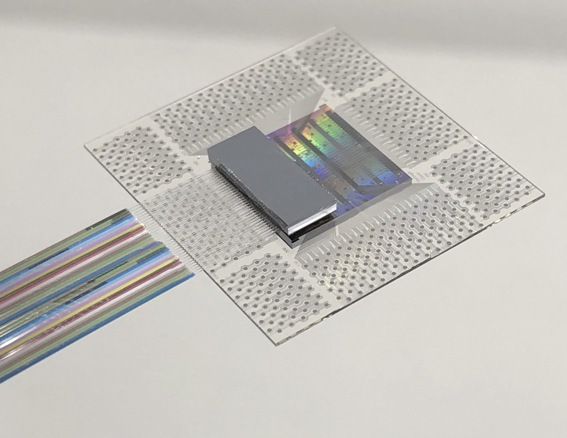
Nubis’ first product is the XT1600 optical module. Here, a substrate houses the company’s PIC and electronics onto which is packaged a lid containing the optical fibres.
Nubis has developed in-house the packaging and the fibre attach solution.
The substrate is 15x15mm, somewhat larger than the engine. Harding says this is deliberate to support products under development.
The 1.6 terabits – in fact, 16x112Gbps full duplex – module has a 2km reach. Its power consumption is below 4 pJ/b.
The fibres exit the module vertically and bend to the side. “[Going] vertical is good but the 2D is the much more important aspect here,” says Winzer.
A 2D approach is logical, says Nubis. An electrical ball grid array (BGA) all the bottom surface. It makes sense that the optics is similarly massively 2D, especially for designs where its a 100-gigabit electrical signal in and a 100-gigabit optical signal out.
Multiple rings of optical I/O engines can surround the ASIC because the fibres exit vertically. “Nobody else can do that because they are escaping from the [PIC] edge,” says Winzer.
Winzer highlights another benefit of the design.
The Universal Chiplet Interconnect Express (UCIe) specification calls for 2T/mm bandwidth escape density. An optical chiplet can only achieve this if wavelength-division multiplexing (WDM) is used due to the large fibre size. Nubis can achieve this density optically without having to use WDM because of 2D surface coupling.
Doing all-to-all at scale remains a big system challenge. “We’re just a part of that challenge,” says Harding. But for optical I/O to become pervasive in the data centre over the next five years, the optics must be significantly lower power, smaller, and efficient.
“If you crack that 2D nut, you can do many, many great things down the road,” says Winzer. “We’ve solved a huge technology problem that allows us to scale much better than anybody else.”
Status
Nubis has not named its foundry and contract manufacturing partners but says they are large, high-volume manufacturers.
Harding says there are now up to five credible silicon photonic foundries available.
“There was some early product definition which some foundries were better suited to support,“ says Harding. “And there was a robustness of the initial PDKs [process design kits] to get us an early product that was important to us.”
Choosing a contract manufacturer proved easier, given the maturity of the players.
Nubis’ first product has 16 optical channels each at 112 gigabit, but future designs will offer N by 224-gigabit channels.
Meanwhile, the XT1600 optical engine is available for sampling.

Teramount brings pluggability to co-packaged optics
Hesham Taha, the CEO and co-founder of Teramount, describes the last two years for his company as eventful.
“Many things have happened on many fronts,” he says.
Teramount has developed a fibre assembly technology for designs integrating photonics and chips.
The start-up has raised $20 million in funding and has 30 staff. In addition, the company is recruiting staff experienced in manufacturing processes.
“The funding helps to support what we are working on today, which is manufacturing readiness,” says Taha.
Taha also notes marketplace changes as when the rising interest in co-packaged caused some companies that had stepped out of silicon photonics to return.
The marketplace moves reflect silicon photonics’ changing role. The technology is central for integrated designs such as co-packaged optics, whereas before, it had a more peripheral role when used for pluggable optics.
“This is a big change that requires optical integration with electronics, a change in packaging, and how you assemble fibres,” says Taha.
Plugs and bumps
Teramount’s technology coupling fibre to silicon photonics chips has two elements: a photonic bump and a photonic plug. The two combined avoid having to bond the fibre to the chip directly.
This is important for two reasons.
First, fibre bonding is an extra manufacturing step that impacts adversely the yield of an expensive chip.
Second, the plug, which is on a separate plane from the chip, working together with the photonic bump, enables the fibres to be detached and serviced, much like pluggable optics.
The photonic plug holds the fibres using a V-groove mechanism and couples them to the silicon photonics chip via the photonic bump, a component manufactured as part of the silicon photonics design.
It is the plug and bump combined that deliver large assembly tolerances. “The large tolerances is what enables the detachability,” says Taha.
It means a semiconductor company can avoid dealing with fibres and focus on what it does best: designing chips. Foundries and outsourced semiconductor assembly and test (OSAT) companies can handle the wafer-level plug and connect the fibres.
“If the right foundations are set on the silicon photonics wafer, then silicon photonics packaging can become very easy with detachable optics,” says Taha.
Surface coupling and edge coupling
Silicon photonics uses two approaches to couple the optical signal from the fibre to a photonics chip.
One, known as surface coupling, uses a grating coupler, while the second uses side coupling.
Grating couplers are wavelength dependent and send the light beam out at a specific angle. Therefore, changing the wavelength affects the angle, complicating the interfacing.

As part of the silicon photonics chip design, the photonic bump – effectively a lens – is positioned accurately next to the grating coupler.
In contrast, side coupling collects the beam for the silicon photonic chip’s waveguide from the edge of the die. Here, there is no spectral dependency. “You can inject in and out multiple wavelengths,” says Taha.
Teramount says side coupling is not viable for the volume manufacturing of silicon photonic designs.
“You cannot connect a fibre from the edge of the die; you have to prepare for a photonic bump before wafer dicing for side coupling,” says Taha.
Teramount’s design enables light to go to the side of the die, but instead of collecting it from the edge, the photonic bump deflects the beam vertically.
“The photonic bump shifts side coupling into the wideband surface coupling,” says Taha.
The photonic bump has two components in the wideband surface coupling case: a wideband deflector and a lens mirror for beam expansion.
The photonic bump and plug combined forms what Teramount calls self-aligning optics. “You have added more complexity in wafer-level manufacturing, but you have relaxed the tolerances in the assembly domain,” he says.
The resulting design has assembly tolerances of +/- 30 microns. “Altogether, over 60 microns, you lose only half a dB in misalignment tolerances,” he says.
Teramount supports both solutions: surface coupling for a single wavelength and wideband surface coupling for multiple wavelengths. Most customers are working with the wideband solution, says Taha.
The assembly tolerances, wideband surface coupling, and planar separation of the fibres from the die, are what enable fibre detachability, says Taha.
“A technician can manually assemble hundreds of fibres on a co-packaged optics stack,” he says.
The fibre assembly process is compatible with semiconductor packaging techniques. No fibre reflow soldering is needed, improving co-packaged optics’ yield while enabling the servicing of the fibre assembly for co-packaged optics.
Status
Teramount announced in 2022 a collaboration with EV Group, an equipment and process solutions supplier, to tackle wafer-level optics.
Taha says Teramount is working with foundries, OSATs and wafer-level optics manufacturers, such as EV group, to create an ecosystem for its photonic bump and photonic plug technology.
“We want the customer to have the ability to use a foundry to include in their wafer a photonic bump,” says Taha. “Once there, a customer can enjoy the photonic plug connector, its relaxed assembly tolerances, and detachable fibre connectivity.”
Teramount is also working with vendors in networking and computing, developers of co-packaged optics and optical input-output for processor clusters used for machine learning, respectively.
“We’ve already sent samples to customers that we are working with, which includes 32 fibres,” says Taha.
Teramount intends to announce more collaborations with vendors and wafer-manufacturing suppliers.
OFC 2023 show preview
- Sunday, March 5 marks the start of the Optical Fiber Communication (OFC) conference in San Diego, California
- The three General Chairs – Ramon Casellas, Chris Cole, and Ming-Jun Li – discuss the upcoming conference
OFC 2023 will be a show of multiple themes. That, at least, is the view of the team overseeing and coordinating this year’s conference and exhibition.
General Chair Ming-Jun Li of Corning who is also the recipient of the 2023 John Tyndall Award (see profiles, bottom), begins by highlighting the 1,000 paper submissions, suggesting that OFC has returned to pre-pandemic levels.
Ramon Casellas, another General Chair, highlights this year’s emphasis on the social aspects of technology. “We are trying not to forget what we are doing and why we are doing it,” he says.
Casellas highlights the OFC’s Plenary Session speakers (see section, below), an invited talk by Professor Dimitra Simeonidou of the University of Bristol, entitled: Human-Centric Networking and the Road to 6G, and a special event on sustainability.
This year’s OFC has received more submissions on quantum communications totaling 66 papers.
In the past, papers on quantum communications were submitted across OFC’s tracks addressing networking, subsystems and systems, and devices. However, evaluating them was challenging given that only some reviewers are quantum experts, says Chris Cole, the third General Chair. Now, OFC has a subcommittee dedicated to quantum.
Another first is OFCnet, a production network that will run during the show.
Themes and topics
Machine learning is one notable topic this year. The subject is familiar at OFC, says Casellas, but people are discussing it more.
Casellas highlights one session at OFC 2021 that addressed machine learning for optics and optics for machine learning. “It showed the duality of how you can use photonic components to do machine learning and apply machine learning to optimise networking,” says Casellas.
This year there will be additional aspects of machine learning for networks, transmission, and operations, says Casellas.
Other General Chair highlighted subjects include point-to-multipoint coherent transmission, non-terrestrial and satellite networks, and optical switching and how its benefits networking in the data centre.
Google, for example, is presenting a paper detailing its use of optical switching in its data centres, something the hyperscaler disclosed at the ACM Sigcomm conference in August 2022.
There is also more interest in fibre sensors used in communications networks.
“We see an increasing trend because now if you want smart networks, you need sensors everywhere,” says Li.
“That is another theme that goes across all the tracks, which is a non-traditional optical fibre communication area that we’ve been embracing,” adds Cole.
As examples, Cole cites lidar, radio over fibre, free-space communications, microwave fibre sensing, and optical processing.
OFC has had contributions in these areas, he says, but now these topics have dedicated subcommittee titles.
Plenary session
This year’s three Plenary Session speakers are:
- Patricia Obo-Nai, CEO of Vodafone Ghana, who will discuss Harnessing Digitalization for Effective Social Change,
- Jayshree V. Ullal, president and CEO of Arista Networks, addressing The Road to Petascale Cloud Networking,
- and Wendell P. Weeks, chairman and CEO of Corning, whose talk is entitled Capacity to Transform.
“We thought that having someone who could explain how technology improves society would be very positive,” says Casellas. “I’m proud to have someone who can talk on the benefits of digitisation from the point of view of society, in addition to more technical topics.”
Li highlights how OFC celebrated the 50th anniversary of low-loss fibre two years ago and that last year, OFC celebrated the year of glass, displaying information on panels.
Corning has played an important role in both technologies. “Having a speaker [Wendell Weeks] from a glass company talking about both will be interesting to the OFC audience,” says Li.
Cole highlights the third speaker, Jayshree Ullal, the CEO of Arista. The successful networking player is one of the companies competing in what he describes as a very tough field.
Rump session
This year’s Rump Session tackles silicon photonics, a session moderated by Daniel Kuchta of IBM TJ Watson Research Center and Michael Hochberg of Luminous Computing.
Cole says silicon photonics has received tremendous attention, and the Rump Session is asking some tough questions: “Is silicon photonics for real now? Is it just one of the guys in the toolbox? Or is it being sunsetted or supplemented?”
Cole expects a lively session, not just challenging conventional thinking but having people representing exciting alternatives which are commercially successful alongside silicon photonics.
Show interests
The Chairs also highlight their interests and what they hope to learn from the show.
For Li, it is high-density fibre and cable trends.
Work on space division multiplexing (SDM) – multicore and multimode – fibre has been an OFC topic for over 15 years. One question Li has is whether systems will use SDM.
“It looks like multicore fibre is close, but we want to learn more from customers,” says Li.
Another interest is an alternative development of reduced coating diameter fibres that promise greater cable density. “I always think this is probably the short-term solution, but we’ll see what people think,” says Li.
AI drives interest in fibre density and latency issues in the data centre. Low latency is attracting interest in hollow-core fibre. Microsoft acquired Lumenisity, a UK hollow core fibre specialist, late last year.
Li is keen to learn more about quantum communications. “We want to understand, from a fibre component point of view, what to do in this area.”
Until now industry focus has been on quantum key distribution (QKD), but Li wants to learn about other applications of quantum in telecoms.
The bandwidth challenge facing datacom is Cole’s interest.
As the Rump Session shows, there has been an explosion of technologies to address data challenges, particularly in the data centre. “So I’m looking forward to continuing to see all the great ideas and all the different directions,” says Cole.
Another show interest for Cole is start-ups in components, subsystems and systems, and networking.
At Optica’s Executive Forum, held on Monday, March 6, a session is dedicated to start-ups. Casellas is looking forward to the talks on optical network automation.
Much work has applied machine learning to optical transmission and amplifier optimisation. Casellas wants to see how reinforcement learning is applied to optical network controllers. Telemetry and its use for network monitoring are another of his interests.
“Maybe because I’m an academic and idealistic, but I like everything related to disaggregation and the opening of interfaces,” says Casellas, who too wants to learn more about quantum.
“I have a basic understanding of this, but maybe it is hard to get into something new,” says Casellas. Non-terrestrial and satellite networks are other topics of interest.
Cole concludes with a big-picture view of photonics.
“It’s a great time to be in optics,” he says. “We’re seeing an explosion of creativity in different areas to solve problems.”
Ramon Casellas works at the Centre Tecnològic de Telecomunicacions de Catalunya (CTTC) research institution in Barcelona, Spain. His research focuses on networks – particularly the control plane, operations and management – rather than optical systems and devices.
Ming-Jun Li is a Corporate Fellow at Corning where he has that worked for 32 years.
Li is also this year’s winner of the John Tyndall Award, presented by Optica and the IEEE Photonics Society. The award is for Li’s ‘seminal contributions to advances in optical fibre technology.’
“It was a surprise to me and a great honour,” says Li. “The work is not only for myself but for many people working with me at Corning; I cannot achieve without working with meaningful colleagues.”
Chris Cole is a consultant whose background is in datacom optics. He will be representing the company, Coherent, at OFC.
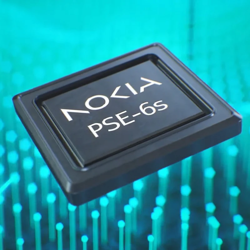
Nokia jumps a class with its PSE-6s coherent modem
- The 130 gigabaud (GBd) PSE-6s coherent modem is Nokia’s first in-house design for high-end optical transport systems
- The PSE-6s can send an 800 gigabit Ethernet (800GbE) payload over 2,000km and 1.2 terabits of data over 100km.
- Two PSE-6s DSPs can send three 800GbE signals over two 1.2-terabit wavelengths
Nokia has unveiled its latest coherent modem, the super coherent Photonic Service Engine 6s (PSE-6s) that will power its optical transport platforms in the coming years.
The PSE-6s comes three years after Nokia announced its current generation of coherent digital signal processors (DSPs): the PSE-Vs DSP for the long-haul and the compact PSE-Vc for the coherent pluggable market.
Nokia is only detailing the PSE-6s; its next-generation coherent modem for pluggables will be a future announcement.
Nokia will demonstrate the PSE-6s at the upcoming OFC show in March while field trials involving systems using the PSE-6s will start in the year’s second half.
Reducing cost per bit
In 2020, Nokia bought Elenion, a silicon photonics company specialising in coherent optics.
The PSE-6s is Nokia’s first in-house coherent modem – the coherent DSP and associated optics – targeting the most demanding optical transport applications.
Nokia points out that coherent systems started approaching the Shannon limit two generations ago.
In the past, operators could reduce the cost of optical transport by sending more data down a fibre; upgrading the optical signal from 100 to 200 to 400 gigabit required only a 50GHz channel.
“You were getting more fibre capacity with each generation,” says Serge Melle, director of product marketing, optical networks at Nokia. And this helped the continual reduction of the cost-per-bit metric.
But with more advanced DSPs, implemented using 16nm, 7nm, and now 5nm CMOS, going to a higher symbol rate and hence data rate requires more spectrum, says Melle.
Increasing the symbol rate is still beneficial. It allows more data to be sent using the same modulation scheme or transmitting the same data payload over longer distances.
“So one of the things we are looking to do with the PSE-6s is how do we still enable a lower total cost of ownership even though you don’t get more capacity per wavelength or fibre,” says Melle.

Symbol rate classes
Coherent optics from the leading vendors use a symbol rate of 90-107 gigabaud (GBd), while Cisco-owned Acacia’s latest 1.2-terabit coherent modem in a CIM-8 module operates at 140GBd.
Acacia uses a classification system based on symbol rate. First-generation coherent systems operating at 30-34GBd are deemed Class 1. Class 2 doubles the baud rates to 60-68GBd, the symbol rate window used for 400ZR coherent optics, for hyperscalers to connect equipment across their data centres up to 120km apart.
The DSPs from the leading optical transport systems vendors operating at 90-107GBd are an intermediate step between Class 2 and Class 3 using Acacia’s classification. In contrast, Acacia has jumped directly from Class 2 to Class 3 with its 140GBd CIM-8 coherent modem.
Competitors view Acacia’s classification scheme as a marketing exercise and counter that their 90-107GBd optical transport systems benefited customers for over two years.
Nokia’s 90GBd PSE-Vs can send 400 gigabits using quadrature phase-shift keying (QPSK) over 3,000km. This contrasts with its earlier 67GBd PSE-3s that sends 400GbE up to 1,000km using 16-QAM.
However, with the PSE-Vs, Nokia, unlike its optical transport competitors, Infinera, Ciena and Huawei, decided not to support 800-gigabit wavelengths.
Nokia argued that 7nm CMOS, 90-100GBd coherent optics tops out at 600 gigabit when used for distances of several hundred kilometers, while metro-regional distances are more economically served using 400-gigabit pluggable optics such as the CFP2 implementing 400ZR+.
With the 130Gbd PSE-6s, Nokia has a Class 3 coherent modem with the PSE-6s capable of sending 800 gigabits more than 2,000km.
The PSE-6s also doubles the maximum data rate of the PSE-Vs to 1.2 terabits per wavelength. However, at 1.2 terabits, the reach is 100-plus km, valuable for very high capacity metro transport and data centre interconnect.
Scale, reach and power consumption per bit
Nokia highlights the PSE-6s’ main three performance metric improvements.
First, the coherent modem delivers scaling: two coherent optical engines fit on a line card to deliver 2.4 terabits to transport emerging high-speed services such as 800GbE.
The two PSE-6s are linked using a dedicated interface to share the client-side signals (see diagram).
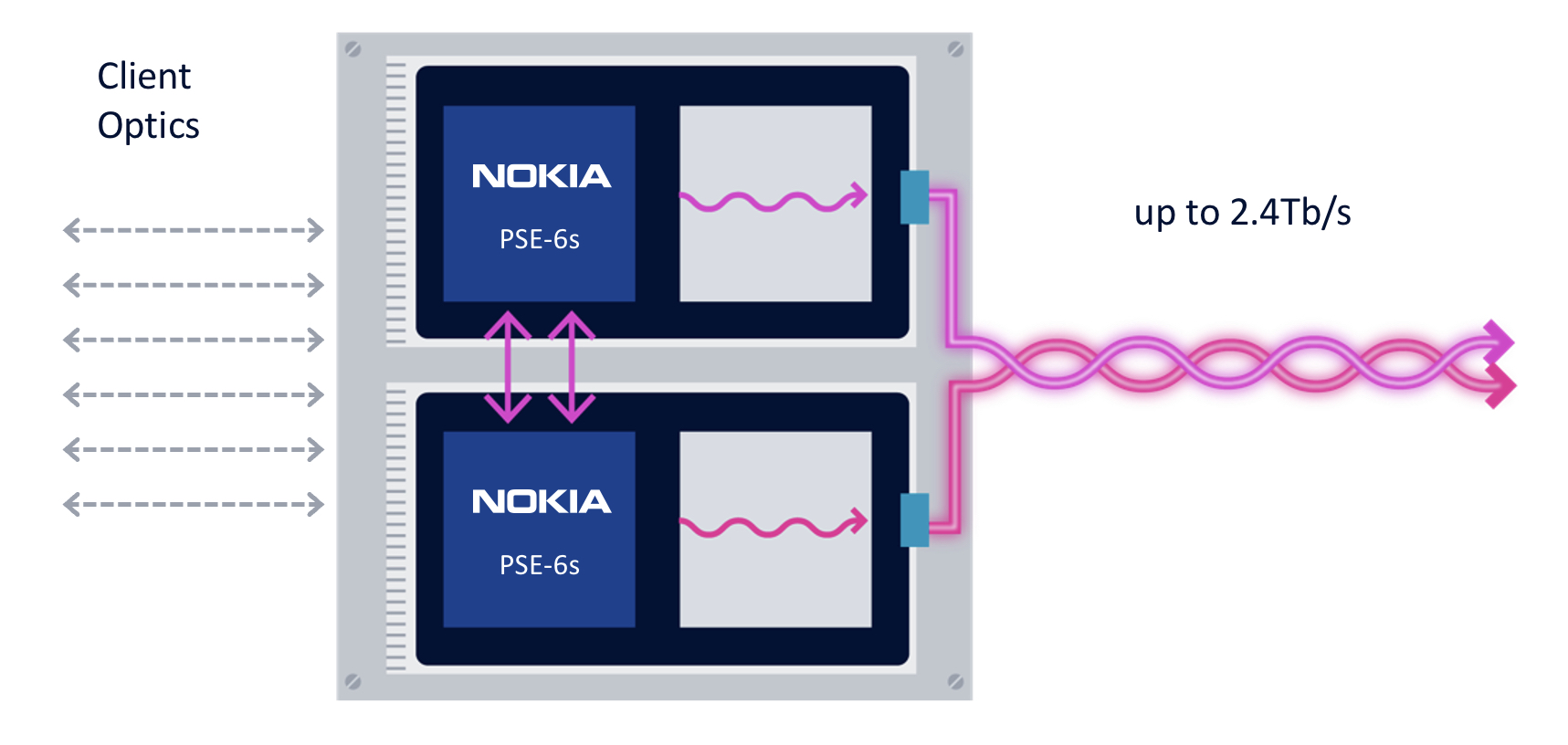
“We are not the only ones introducing a 5nm solution, but I think we are the only ones that allow two DSPs to work together,” says Melle.
Without the interface, a single 800GbE and up to four 100GbE clients or a 400GbE client can be sent over each DSP’s 1.2-terabit wavelength. Adding the interface, an operator can send three uniform 800GbE clients, with the interface splitting the third 800GbE client between the two DSPs.
“In a single line card, you can stripe the three 800-gigabit services rather than have to deploy three separate line cards in the network,” says Melle.
Nokia is not detailing the interface used to link the DSPs but said that the interface is used for data only and not to share signal processing resources between the ASICs.
“There is an extra amount of circuitry to share the client bandwidth across the two DSPs, but it is not high power consuming, and most transponders have some circuitry between the clients and the DSP,” says Melle. “So the incremental ‘power tax’ is marginal; it doesn’t add any significant power overhead.”
The resulting 2.4-terabit transmission is sent as two 1.2-terabit wavelengths, each occupying a 150GHz-wide channel. Existing systems that operate at 90-107GBd typically use a 112.5GHz channel for an 800-gigabit transmission, so the PSE-6s delivers a fibre capacity benefit.
The two wavelengths can be bonded, as in a two-channel ‘super-channel’, or sent to separate locations.
The second improvement is optical performance. For example, an 800-gigabit payload can travel over 2,000km. Nokia claims this is 3x the reach of existing commercial optical transport systems.
The improved transmission performance is achieved using a combination of the 130GBd baud rate, probabilistic constellation shaping (PCS), and improved forward error correction (FEC). Melle says the contributions to the improvement are 90 per cent baud rate and 10 per cent due to coherent modem algorithm tweaks.
“Baud rate is king; that is what really drives this improved performance,” says Melle.
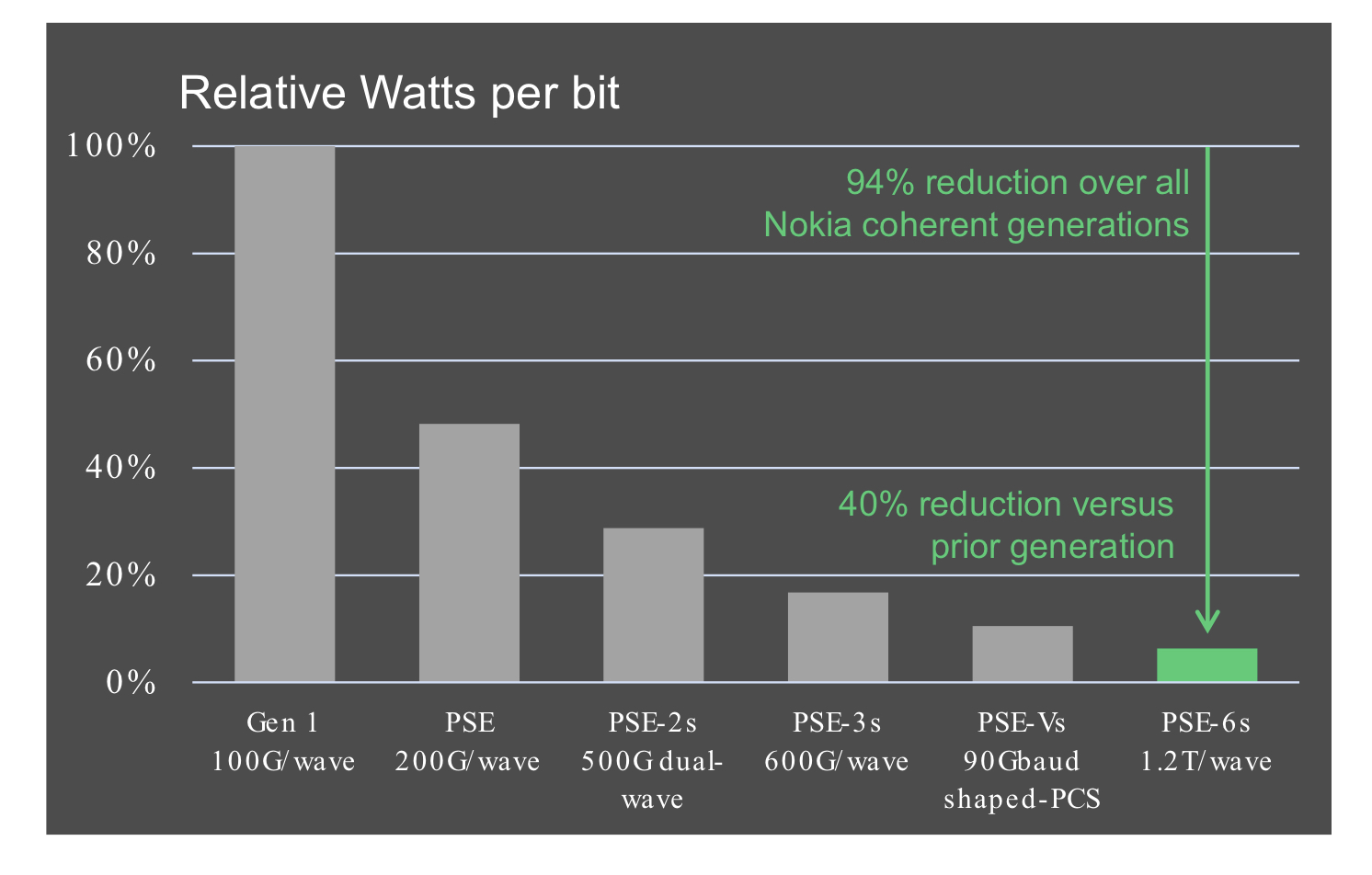
The third benefit is reduced power consumption at the device and system (networking) levels.
Using a 5nm finFET CMOS process to make the PSE-6s DSP ASIC and developing denser line cards (two modems per card) means systems will consume 60 per cent less power than Nokia’s existing coherent technology.
According to Nokia, the PSE-6s optical engine consumes 40 per cent fewer Watts per bit compared to the PSE-Vs.
Nokia 1830 transport systems
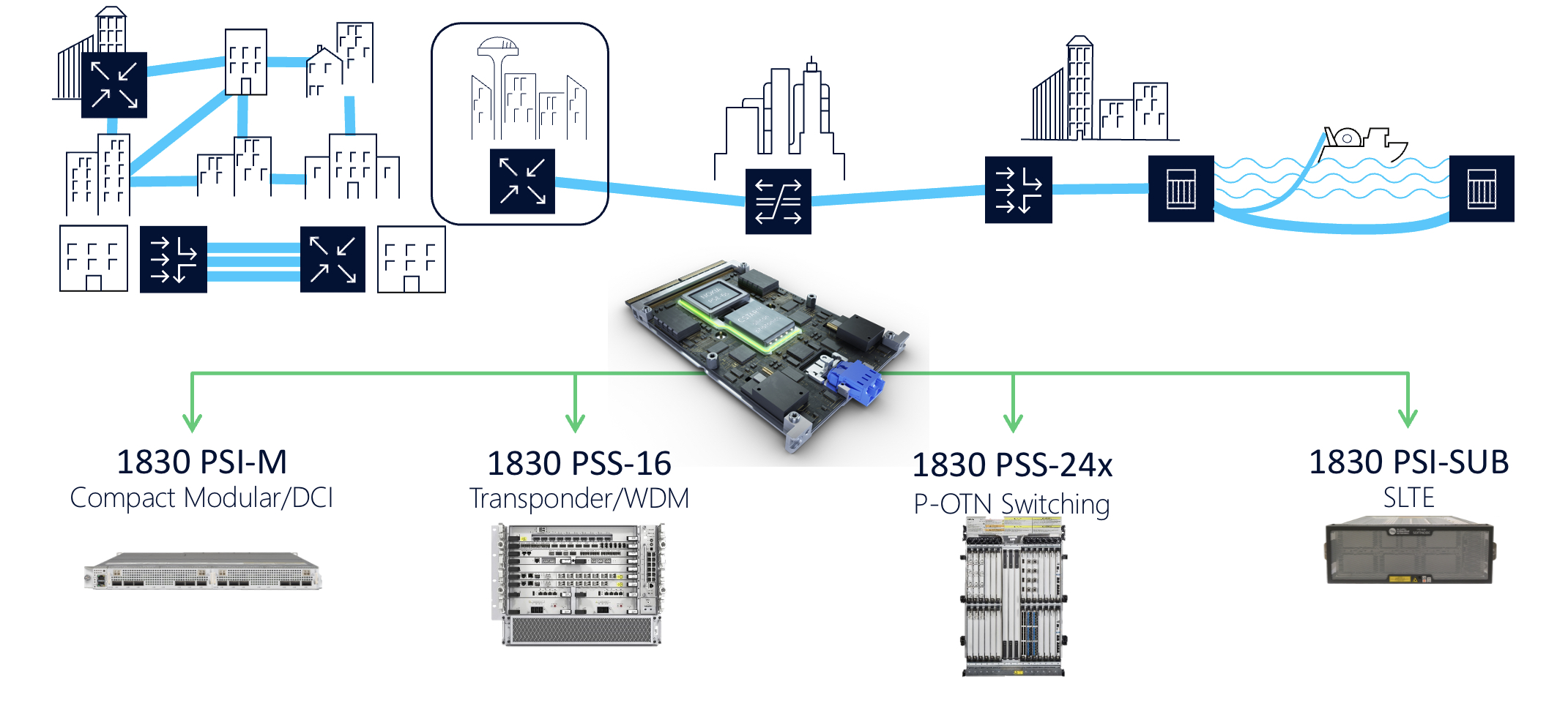
The PSE-6s line cards fit into Nokia’s existing range of 1830 transport platforms.
These include the 1830 PSI-M compact modular data centre interconnect, the 1830 PSS-16 transponder and WDM line system, the 1830 PSS-24x P-OTN and switching chassis, and the 1830 PSI-SUB subsea line-terminating equipment.
For example, the PSI-M platform can hold two line cards, each with two PSE-6s.

Tencent makes its co-packaged optics move

- Tencent is the first hyperscaler to announce it is deploying a co-packaged optics switch chip
- Tencent will use Broadcom’s Humboldt that combines its 25.6-terabit Tomahawk 4 switch chip with four optical engines, each 3.2 terabit-per-second (Tbps)
Part 2: Broadcom’s co-packaged optics
Tencent will use Broadcom’s Tomahawk 4 switch chip co-packaged with optics for its data centres.
“We are now partnered with the hyperscaler to deploy this in a network,” says Manish Mehta, vice president of marketing and operations optical systems division, Broadcom. “This is a huge step for co-packaged optics overall.”
Broadcom demonstrated a working version of a Humboldt switch at OFC earlier this year.
The Chinese hyperscaler will use Broadcom’s 25.6Tbps Tomahawk 4 Humboldt, a hybrid design where half of the chip’s input-output (I/O) is optical and half is the chip’s serialisers-deserialisers (serdes) that connect to pluggable modules on the switch’s front panel.
Four Broadcom 3.2-terabit silicon photonics-based optical engines are co-packaged alongside the Tomahawk 4 chip to implement 12.8Tbps of optical I/O.
Broadcom demonstrated a working version of a Humboldt switch at OFC earlier this year.
Co-packaged optics
Broadcom started its co-packaged optics development work in 2019.
“One of the reasons for our investment in co-packaged optics was that we did see firsthand the ongoing limits of copper interconnect being approached,” says Mehta.
The transmission reach of copper links continues to shrink as the signalling speed has increased from 25 gigabits-per-second (Gbps) non-return to zero (NRZ) to PAM-4 (4-level pulse amplitude modulation) based signalling at 56Gbps, 112Gbps and, in the coming years, 224Gbps. Power consumption is also rising with each speed hike.
Broadcom says data centres now use 1 million optical interconnects, but that much of the connectivity is still copper-based, linking adjacent racks and equipment within the rack.
“Hyperscalers spend ten times more on interconnects than switching silicon,” says Mehta. Given these trends, there needs to be a continual improvement in the power profile, cost and scaled manufacturing of optical interconnect, he says.
In the short term, what is driving interest in co-packaged optics is overcoming the limitations of copper, says Broadcom.
In early 2021, Broadcom detailed at a JP Morgan event its co-packaged optics roadmap. Outlined was the 25.6-terabit Humboldt to be followed by Bailly, a 51.2-terabit all co-packaged optics design using Broadcom’s Tomahawk 5 switch chip which is now sampling.
Humboldt uses DR4 (4×100-gigabit using 4 fibres) whereas the 51.2-terabit Bailly will add multiplexing-demultiplexing and use the FR4 specification (4×100-gigabit wavelengths per fibre).
Technology and partners
Broadcom’s in-house technology includes lasers (VCSELs and EMLs), mixed-signal expertise (trans-impedance amplifiers and drivers), and silicon photonics, as well as its switch chips.
Broadcom uses a remote laser source for its co-packaged optics design. Placing the laser away from the package (the switch chip and optics) means no cooling is needed.
Broadcom is working with 15 partners to enable its co-packaged optics, highlighting the breadth of expertise required and the design complexity.
There are two prominent use cases for the hybrid I/O Humboldt.
One is for top-of-rack switches, where the electrical interfaces support short-reach copper links connecting the servers in a rack, while the optical links connect the top-of-rack box to the next layer of aggregation switching.
The second use is at the aggregation layer, where the electrical I/O connects other switches in the rack while the optical links connect to switch layers above or below the aggregation layer.
“There is a use case for having pluggable ports where you can deploy low-cost direct-attached copper,” says Mehta.
Broadcom says each data centre operator will have their own experience with their manufacturing partners as they deploy co-packaged optics. Tencent has decided to enter the fray with 25.6-terabit switches.
“It is not just Broadcom developing the optical solution; it is also ensuring that our manufacturing partner is ready to scale,” says Mehta.
Ruijie Networks is making the two-rack-unit (2RU) switch platform for Tencent based on Broadcom’s co-packaged optics solution. The co-packaged optics interfaces are routed to 16 MPO connectors while the switch supports 32, 400-gigabit QSFP112 modules.
“It’s always important to have your lead partner [Tencent] for any deployment like this, someone you’re working closely with to get it to market,” says Mehta. “But there is interest from other customers as well.”
Cost and power benefits
Broadcom says co-packaged optics will lower the optical cost-per-bit by 40 per cent while the system (switch platform) power savings will be 30 per cent.
Humboldt more than halves the power compared to using pluggables. Broadcom’s co-packaged optics consumes 7W for each 800-gigabits of bandwidth, whereas an equivalent 800-gigabit optical module consumes 16-18W.
Its second-generation design will embrace 5nm CMOS rather than 7nm and still more than halve the power: an 800-gigabit pluggable will consume 14-15W, whereas it will be 5.5W for the same co-packaged optics bandwidth.
Broadcom will move to CMOS for its second-generation electrical IC; it uses silicon germanium at present.
Power and operational cost savings are a longer-term benefit for data centre operators, says Broadcom. A more immediate concern is the growing challenge of managing the thermal profile when designing switching systems. “The amount of localised heat generation of these components is making systems quite challenging,” says Mehta.
A co-packaged design eliminates pluggables, making system design easier by improving airflow via the front panel and reducing the power required for optical interconnect.
“They’ve been telling us this directly,” says Mehta. “It’s been a pretty good testimonial to the benefits they can see for system design and co-packaged optics.”
Roadmap
At OFC 2022, Broadcom also showed a mock-up of Bailly, a 51.2 terabit switch chip co-packaged with eight 6.4Tbps optical engines.
Broadcom will offer customers a fully co-packaged optics Tomahawk 5 design but has not given a date.
Since Broadcom has consistently delivered a doubling of switch silicon capacity every 24 months, a 102.4-terabit Tomahawk 6 is scheduled to sample in the second half of 2024.
That timescale suggests it will be too early to use 224Gbps serdes being specified by the OIF. Indeed, Mehta believes 112Gbps serdes will have “a very long life”.
That would require the next-generation 102.2Tbps to integrate 1024, 100Gbps serdes on a die. Or, if that proves too technically challenging, then, for the first time, Broadcom’s switching ASIC may no longer be a monolithic die.
Broadcom’s networking group is focused on high-speed serial electrical interfaces. But the company is encouraged by developments such as the open standard UCIe for package interconnect, which looks at slower, wider parallel electrical interfaces to support chiplets. UCIe promises to benefit co-packaged optics.
Broadcom’s view is that it is still early with many of these design challenges.
“Our goal is to understand when we need to be ready and when we need to be launching our silicon on the optical side,” says Mehta. “That’s something we are working towards; it’s still not clear yet.”

OpenLight's integrated-laser silicon photonics platform

- OpenLight is an independent silicon photonics company backed by Synopsys and Juniper Networks
- The company was created by carving out the silicon photonics arm of Juniper
- The establishment of OpenLight and its open platform highlights the growing maturity of silicon photonics as new applications emerge beyond datacom and telecom
OpenLight is coming to market with an open silicon photonics platform that includes integrated lasers and gain blocks.
Juniper has a long relationship with Synopsys, using its electronic-photonic design automation (EPDA) tools.
So when Juniper said it was spinning out its silicon photonics group, Synopsys was keen to partner. The result is OpenLight, of which Synopsys has a 75 per cent stake costing $67.5 million.
Thomas Mader, OpenLight’s chief operating officer and formerly head of Juniper’s silicon photonics unit, says OpenLight is the first company to offer an open platform that includes monolithically integrated lasers, optical amplifiers and modulators.
Juniper Networks and Synopsys
Juniper gained its silicon photonics technology in 2016 when it acquired Aurrion for $165 million.
Aurrion was a fabless silicon photonics start-up from the University of California, Santa Barbara, with a heterogeneous integration silicon photonics process that includes III-V materials, enabling integrated lasers as part of a photonic circuit.
OpenLight is now making this technology available through its partnership with the foundry Tower Semiconductor.
Juniper’s interests are mainly datacom and telecom, but it recognises the emerging opportunities for silicon photonics such as Lidar, optical computing, high-performance computing and optical interconnect.
“With this kind of technology, you want to drive volumes,” says Mader.

Juniper saw spinning out the unit and opening up access to the technology as the best way to drive volumes and reduce costs. The arrangement also benefits Juniper’s own technology needs.
Synopsys, meanwhile, believes it is the right time to back the OpenLight venture.
“We think it [the open platform] is a great opportunity for growth for Synopsys’s EPDA tools,” says John Koeter, senior vice president of marketing and strategy, solutions group at Synopsys.
OpenLight will give Synopsys insight into how the market is evolving and benefit the company’s tools and, eventually, its IP.
Business model
OpenLight is licensing its process design kit (PDK), the files that model Tower’s fabrication process. A company can enter into an agreement with Tower, access the PDK and design its silicon photonics device.
“What we are offering through Tower, and what we spent significant effort developing and showing Tower how to do, is monolithically integrating lasers and optical gain,” says Mader. “Tower is the first time we’re on a volume eight-inch [wafer] process.”
Juniper entered into a partnership with Tower Semiconductor in 2019.
“We are doing the first MPW [multi-project wafer] this summer with Tower on this process,” says Mader.
OpenLight is also providing designs it has developed and validated for several customers. “But we are not selling PICs [photonic integrated circuits]; that is not part of our plan,” says Mader.
OpenLight intends to partner with other foundries to make more widely available integrated-laser designs.

For now, though, OpenLight is focussed on ratifying its roadmap for the next two years.
“We’re going to be busy building out the component library for Tower to keep customers interested because better components make better circuits,” says Daniel Sparacin, vice president of business development and strategy at OpenLight.
OpenLight offers a 100-gigabit modulator and is working on its next-generation 200-gigabit modulator.
“We’re mostly O-band right now, and we have C-band coming up in the roadmap very shortly,” says Sparacin.
Applications
OpenLight has 400 and 800-gigabit optical designs for the data centre to help customers bring to market their PIC developments.
The company is also seeing interest from Lidar customers, particularly those pursuing coherent-based designs.
“The main reason is the integrated laser,” says Mader. “Otherwise, with standard silicon photonics, you have to attach a laser separately, which doesn’t scale well to multiple channels.” That’s because attaching multiple lasers impacts yield.
Lidar also benefits from on-chip optical amplification. “When you have a complex chip, you have a lot of losses,” says Mader.
OpenLight is working with firms pursuing optical computing for machine learning which promises greater power efficiency. “There are several of them coming to us because we can put hundreds or thousands of indium phosphide elements monolithically on a chip,” says Mader.
OpenLight says it has no position regarding co-packaged optics and whether a design uses an external light source or integrated lasers.
It believes co-packaged optics designs will eventually use integrated light sources, but its technology supports both and can even be used to make external light sources.
Overall, OpenLight says it is working with dozens of companies.
Design tools and integration
Synopsys has been an early mover with its integrated optical design automation tools. The tools include:
- OptoCompiler, a photonic IC design environment.
- The OptSim photonic circuit and system simulator.
- The Sentaurus TCAD and RSoft Photonic Device tools for process modelling and device design.
Working closely with OpenLight will benefit Synopsys’s tool environment, says Koeter. Synopsys is adding functionalities and design capabilities to its tools to support the integration of lasers. OpenLight is also providing Synopsys feedback on what will improve the experience of using its design platform.
Synopsys is one of three leading electronic design automation (EDA) tool companies. However, design tools for photonics are a more recent development.
“EDA quite a while ago is where photonic design is now going,” says Mader.
Integration is the underlying trend driving optics.
“We see the scaling already with 400- and 800-gigabit for datacom and some of the other applications; you see the shift to silicon photonics,” says Mader. “The higher the complexity, the more you see it shifting this way because there’s a cost advantage with the integrated laser and optical gain.”
Photonics may not come close to chip designs with billions of transistors. Still, photonic designs that go beyond four-channel design to ones with 32 or 64 channels or optical computing with hundreds or thousands of components are emerging.
“So you see a scaling even though it’s decades behind the electronics field,” says Mader.
With monolithically integrated lasers, yields remain high, whereas scaling a design with discrete components results in unacceptable yields.
“And so we will be able to go where you can’t go otherwise,” says Mader. “It’s not billions, but even dozens [of components] at this point is revolutionary.”

Intel adds multi-channel lasers to its silicon photonics toolbox
Intel has developed an 8-lane parallel-wavelength laser array to tackle the growing challenge of feeding data to integrated circuits (ICs).
Optical input-output (I/O) promises to solve the challenge of getting data into and out of high-end silicon devices.
These ICs include Ethernet switch chips and ‘XPUs’, shorthand for processors (CPUs), graphics processing units (GPUs) and data processor units (DPUs).
The laser array is Intel’s latest addition to its library of silicon photonics devices.
Power wall
A key challenge facing high-end chip design is the looming ‘power wall’. The electrical I/O power consumption of advanced ICs is rising faster than the power the chip consumes processing data.
James Jaussi, senior principal engineer and director, PHY research lab at Intel Labs, says if this trend continues, all the chip’s power will be used for communications and none will be left for processing, what is known as the power wall.
One way to arrest this trend is to use optical rather than electrical I/O by placing chiplets around the device to send and receive data optically.
Using optical I/O simplifies the electrical I/O needed since the chip only sends data a short distance to the adjacent chiplets. Once in the optical domain, the chiplet can send data at terabit-per-second (Tbps) speeds over tens of meters.
However, packaging optics with a chip is a significant design challenge and changes how computing and switching systems are designed and operated.

Laser array
Intel has been developing silicon photonics technology for two decades. The library of devices includes ring-resonators used for modulation and detection, photo-detectors, lasers, and semiconductor optical amplifiers.

Intel can integrate lasers and gain blocks given its manufacturing process allows for the bonding of III-V materials to a 300mm silicon wafer, what is known as heterogeneous integration.
The company has already shipped over 6 million silicon photonics-based optical modules – mainly its 100-gigabit PSM-4 and 100-gigabit CWDM-4 – since 2016.
Intel also ships such modules as the 100G LR4, 100G DR/FR, 200G FR4, 400G DR4 and 400G FR4. The company says it makes two million optical modules a year.
Now Intel Labs has demonstrated a laser array that integrates eight distributed feedback (DFB) lasers for wavelength-division multiplexing (WDM) transmissions. In addition, the laser array is compliant with the CW-WDM multi-source agreement.
“This is a much more difficult design,” says Haisheng Rong, senior principal engineer, photonics research at Intel Labs. “The challenge here is that you have a very small channel spacing of 200GHz.”
Each laser’s wavelength is defined by the structure of the silicon waveguide – less than 1 micron wide and tens of microns long – and the periodicity of a Bragg reflector grating.
The lasers in the array are almost identical, says Rong, their difference being defined by the Bragg grating’s period. There is a 0.2nm difference in the grating period of adjacent – 200GHz apart – lasers. For 100GHz spacing, the grating period difference will need to be 0.1nm.
Specifications
The resulting eight wavelengths have uniform separation. Intel says each wavelength is 200GHz apart with a tolerance of plus or minus 13GHz, while the lasers’ output power varies by plus or minus 0.25dB.
Such performance is well inside the CW-WDM MSA specifications that call for a plus or minus 50GHz tolerance for 200GHz channel spacings and plus or minus 1dB variability in output power.
Rong says that using a 200GHz channel enables a baud rate of 64 gigabaud (GBd) or 128GBd. Intel has already demonstrated its electronic and photonic ICs (EIC/ PIC) operating at 50 gigabit-per-second (Gbps) and 112Gbps.
In future, higher wavelength counts – 16- and 32-channel designs – will be possible, as specified by the CW-WDM MSA.
The laser array’s wavelengths vary with temperature and bias current. For example, the laser array operates at 80oC, but Intel says it can work at 100oC.
Products
The working laser array is the work of Intel Labs, not Intel’s Silicon Photonics Products Division. Intel has yet to say when the laser array will be adopted in products.
But Intel says the technology will enable terabit-per-second (Tbps) transmissions over fibre and reach tens of meters. The laser array also promises 4x greater I/O density and energy efficiency of 0.25 picojoules-per-bit (pJ/b), two-thirds that of the PCI Express 6.0 standard.
Another benefit of optical I/O is low latency, under 10ns plus the signal’s time of flight, determined by the speed of light in the fibre and the fibre’s length.
An electrical IC is needed alongside the optical chiplet to drive the optics and control the ring-resonator modulators and lasers. The chip uses a 28nm CMOS process and Intel is investigating using a 22nm process.
Optical I/O goals
Intel announced in December 2021 that it was working with seven universities as part of its Integrated Photonics Research Center.
The goal is to create building-block circuits that will meet optical I/O needs for the next decade-plus, says Jaussi.
Intel aims to demonstrate by 2024 sending 4Tbps over a fibre while consuming 0.25pJ/b.

II-VI’s VCSEL approach for co-packaged optics
Co-packaged optics was a central theme at this year’s OFC show, held in San Diego. But the solutions detailed were primarily using single-mode lasers and fibre.
The firm II-VI is beating a co-packaged optics path using vertical-cavity surface-emitting lasers (VCSELs) and multi-mode fibre while also pursuing single-mode, silicon photonics-based co-packaged optics.
For multi-mode, VCSEL-based co-packaging, II-VI is working with IBM, a collaboration that started as part of a U.S. Advanced Research Projects Agency-Energy (ARPA-E) project to promote energy-saving technologies.
II-VI claims there are significant system benefits using VCSEL-based co-packaged optics. The benefits include lower power, cost and latency when compared with pluggable optics.
The two key design decisions that achieved power savings are the elimination of the retimer chip – also known as a direct-drive or linear interface – and the use of VCSELs.
The approach – what II-VI calls shortwave co-packaged optics – integrates the VCSELs, chip and optics in the same package.
The design is being promoted as first augmenting pluggables and then, as co-packaged optics become established, becoming the predominant solution for system interconnect.
For every 10,000 QSFP-DD pluggable optical modules used by a supercomputer that are replaced with VCSEL-based co-packaged optics, the yearly electricity bill will be reduced by up to half a million dollars, estimate II-VI and IBM.
VCSEL technology
VCSELs are used for active optical cables and short-reach pluggables for up to 70m or 100m links.
VCSEL-based modules consume fewer watts and are cheaper than single-mode pluggables.
Several factors account for the lower cost, says Vipul Bhatt, vice president of marketing, datacom vertical at II-VI.
The VCSEL emits light vertically from its surface, simplifying the laser-fibre alignment, and multi-mode fibre already has a larger-sized core compared to single-mode fibre.
“Having that perpendicular emission from the laser chip makes manufacturing easier,” says Bhatt. “And the device’s small size allows you to get many more per wafer than you can with edge-emitter lasers, benefitting cost.”
The tinier VCSEL also requires a smaller current density to work; the threshold current of a distributed feedback (DFB) laser used with single-mode fibre is 25-30mA, whereas it is 5-6mA for a VCSEL. “That saves power,” says Bhatt.
Fibre plant
Hyperscalers such as Google favour single-mode fibre for their data centres. Single-mode fibre supports longer reach transmissions, while Google sees its use as future-proofing its data centres for higher-speed transmissions.
Chinese firms Alibaba and Tencent use multi-mode fibre but also view single-mode fibre as desirable longer term.
Bhatt says he has been hearing arguments favouring single-mode fibre for years, yet VCSELs continue to advance in speed, from 25 to 50 to 100 gigabits per lane.
“VCSELs continue to lead in cost and power,” says Bhatt. ”And the 100-gigabit-per-lane optical link has a long life ahead of it, not just for networking but machine learning and high-performance computing.“
II-VI says single-mode fibre and silicon photonics modules are suited for the historical IEEE and ITU markets of enterprise and transport where customers have longer-reach applications.
VCSELs are best suited for shorter reaches such as replacing copper interconnects in the data centre.
Copper interconnect reaches are shrinking as interface speeds increase, while a cost-effective optical solution is needed to support short and intermediate spans up to 70 meters.
“As we look to displace copper, we’re looking at 20 meters, 10 meters, or potentially down to three-meter links using active optical cables instead of copper,” says Bhatt. “This is where the power consumption and cost of VCSELs can be an acceptable premium to copper interconnects today, whereas a jump to silicon photonics may be cost-prohibitive.”
Silicon photonics-based optical modules have higher internal optical losses but they deliver reaches of 2km and 10km.
“If all you’re doing is less than 100 meters, think of the incredible efficiency with which these few milliamps of current pumped into a VCSEL and the resulting light launched directly and efficiently into the fibre,” says Bhatt. “That’s an impressive cost and power saving.”
Applications
The bulk of VCSEL sales for the data centre are active optical cables and short-reach optical transceivers.
“Remember, not every data centre is a hyperscale data centre,” says Bhatt. ”So it isn’t true that multi-mode is only for the server to top-of-rack switch links. Hyperscale data centres also have small clusters for artificial intelligence and machine learning.”
The 100m-reach of VCSELs-based optics means it can span all three switching tiers for many data centres.
The currently envisioned 400-gigabit VCSEL modules are 400GBASE-SR8 and the 8-by-50Gbps 400G-SR4.2. Both use 50-gigabit VCSELs: 25 gigabaud devices with 4-level pulse amplitude modulation (PAM-4).
The 400GBASE-SR8 module requires 16 fibres, while the 400G-SR4.2, with its two-wavelength bidirectional design, has eight fibres.
The advent of 100-gigabit VCSELs (50 gigabaud with PAM-4) enables 800G-SR8, 400G-SR4 and 100G-SR1 interfaces. II-VI first demonstrated a 100-gigabit VCSEL at ECOC 2019, while 100-gigabit VCSEL-based modules are becoming commercially available this year.
Terabit VCSEL MSA
The Terabit Bidirectional (BiDi) Multi-Source Agreement (MSA) created earlier this year is tasked with developing optical interfaces using 100-gigabit VCSELs.
The industry consortium will define 800 gigabits interface over parallel multi-mode fibre, the same four pairs of multi-mode fibre that support the 400-gigabit, 400G-BD4.2 interface. It will also define a 1.6 terabit optical interface.
The MSA work will extend the parallel fibre infrastructure from legacy 40 gigabits to 1.6 terabits as data centres embrace 25.6-terabit and soon 51.2-terabit switches.
Founding Terabit BiDi MSA members include II-VI, Alibaba, Arista Networks, Broadcom, Cisco, CommScope, Dell Technologies, HGGenuine, Lumentum, MACOM and Marvell Technology.
200-gigabit lasers and parallelism
The first 200-gigabit electro-absorption modulator lasers (EMLs) were demonstrated at OFC ’22, while the next-generation 200-gigabits directly modulated lasers (DMLs) are still in the lab.
When will 200-gigabit VCSELs arrive?
Bhatt says that while 200-gigabit VCSELs were considered to be research-stage products, recent interest in the industry has spurred the VCSEL makers to accelerate the development timeline.
Bhatt repeats that VCSELs are best suited for optimised short-reach links.
“You have the luxury of making tradeoffs that longer-reach designs don’t have,” he says. “For example, you can go parallel: instead of N-by-200-gig lanes, it may be possible to use twice as many 100-gig lanes.”
VCSEL parallelism for short-reach interconnects is just what II-VI and IBM are doing with shortwave co-packaged optics.
Shortwave co-packaged optics
Computer architectures are undergoing significant change with the emergence of accelerator ICs for CPU offloading.
II-VI cites such developments as Nvidia’s Bluefield data processing units (DPUs) and the OpenCAPI Consortium, which is developing interface technology so that any microprocessor can talk to accelerator and I/O devices.
“We’re looking at how to provide a high-speed, low-latency fabric between compute resources for a cohesive fabric,” says Bhatt. The computational resources include processors and accelerators such as graphic processing units (GPUs) and field-programmable gate arrays (FPGAs).
II-VI claims that by using multi-mode optics, one can produce the lowest power consumption optical link feasible, tailored for very-short electrical link budgets.
The issue with pluggable modules is connecting them to the chip’s high-speed signals across the host printed circuit board (PCB).
“We’re paying a premium to have that electrical signal reach through,” says Bhatt. “And where most of the power consumption and cost are is those expensive chips that compensate these high-speed signals over those trace lengths on the PCB.”
Using shortwave co-packaged optics, the ASIC can be surrounded by VCSEL-based interfaces, reducing the electrical link budget from some 30cm for pluggables to links only 2-3cm long.
“We can eliminate those very expensive 5nm or 7nm ICs, saving money and power,” says Bhatt.
The advantage of shortwave co-packaged optics is better performance (a lower error rate) and lower latency (between 70-100ns) which is significant when connecting to pools of accelerators or memory.
“We can reduce the power from 15W for a QSFP-DD module down to 5W for a link of twice the capacity,” says Bhatt, “We are talking an 80 per cent reduction in power dissipation. Another important point is that when power capacity is finite, every watt saved in interconnects is a watt available to add more servers. And servers bring revenue.”
This is where the 10,000-unit optical interfaces, $0.4-$0.5 million savings in yearly electricity costs comes from.
The power savings arise from the VCSEL’s low drive current, the use of the OIF’s ultra short-reach (USR) electrical interface and the IBM processor driving the VCSEL directly, what is called a linear analogue electrical interface.
In the first co-packaged optics implementation, IBM and II-VI use non-return-to-zero (NRZ) signalling.
The shortwave co-packaged optics has a reach of 20m which enables the potential elimination of top-of-rack switches, further saving costs. (See diagram.)

II-VI sees co-packaged optics as initially augmenting pluggables. With next-generation architectures using 1.6-terabit OSFP-XD pluggables, 20 to 40 per cent of those ports are for sub-20m links.
“We could have 20 to 40 per cent of the switch box populated with shortwave co-packaged optics to provide those links,” says Bhatt.
The remaining ports could be direct-attached copper, longer-reach silicon-photonics modules, or VCSEL modules, providing the flexibility associated with pluggables.
“We think shortwave co-packaged optics augments pluggables by helping to reduce power and cost of next-generation architectures.”
This is the secret sauce of every hyperscaler. They don’t talk about what they’re doing regarding machine learning and their high-performance systems, but that’s where they strive to differentiate their architectures, he says.
Status
Work has now started on a second-generation shortwave design that will use PAM-4 signalling. “That is targeted as a proof-of-concept in the 2024 timeframe,” says Bhatt.
The second generation will enable a direct comparison in terms of power, speed and bandwidth with single-mode co-packaged optics designs.
Meanwhile, II-VI is marketing its first-phase NRZ-based design.
“Since it is an analogue front end, it’s truly rate agnostic,” says Bhatt. “So we’re pitching it as a low-latency, low-power bandwidth density solution for traditional 100-gigabit Ethernet.”
The design also can be used for next-generation PCI Express and CXL disaggregated designs.
II-VI says there is potential to recycle hyperscaler data centre equipment by adding state-of-the-art network fabric to enable pools of legacy processors. “This technology delivers that,” says Bhatt.
But II-VI says the main focus is for accelerator fabrics: proprietary interfaces like NVlink, Fujitsu’s Tofu interconnect or HPE’s Cray’s Slingshot.
“At some point, memory pools or storage pools will also work their way into the hyperscalers’ data centres,” says Bhatt.

Building an AI supercomputer using silicon photonics

- Luminous Computing is betting its future on silicon photonics as an enabler for an artificial intelligence (AI) supercomputer
Silicon photonics is now mature enough to be used to design complete systems.
So says Michael Hochberg (pictured), who has been behind four start-ups including Luxtera and Elenion whose products used the technology. Hochberg has also co-authored a book along with Lukas Chrostowski on silicon photonics design.
In the first phase of silicon photonics, from 2000 to 2010, people wondered whether they could even do a design using the technology.
“Almost everything that was being done had to fit into an existing socket that could be served by some other material system,” says Hochberg.
A decade later it was more the case that sockets couldn’t be served without using silicon photonics. “Silicon photonics had dominated every one of the transceiver verticals that matter: intra data centre, data centre interconnect, metro and long haul,” he says.
Now people have started betting their systems using silicon photonics, says Hochberg, citing the examples as lidar, quantum optics, co-packaged optics and biosensing.
Several months ago Hochberg joined as president of Luminous Computing, a start-up that recently came out of stealth mode after raising $105 million in Series A funding.
Luminous is betting its future on silicon photonics as an enabler for an artificial intelligence (AI) supercomputer that it believes will significantly outperform existing platforms.
Machine learning
The vision of AI is to take tasks that were the exclusively the domain of the human mind and automate them at scale, says Hochberg.
Just in the last decade, the AI community has advanced from doing things using machine learning (ML) that are trivial for humans to tasks that only the most talented experts can achieve.
“We have reached the point where machine learning capabilities are superhuman in many respects,” says Hochberg. “Where they produce results quantifiably better than humans can.”
But achieving such machine learning progress has required huge amounts of data and hardware.
“The training runs for the state-of-the-art recommendation engines and natural language models take tens to hundreds of thousands of GPUs (graphics processing units) and they run from months to years,” says Hochberg.
Moreover, the computational demands associated with machine learning training aren’t just doubling every 18 months, like with Moore’s law, but every 3-4 months. “And for memory demands, it is even faster,” he says.
What that means is that the upper limit for doing such training runs are complete data centres.
Luminous Computing wants to develop AI hardware that scales quickly and simply. And a key element of that will be to use silicon photonics to interconnect the hardware.
“One of the central challenges scaling up big clusters is that you have one kind of bus between your CPU and memory, another between your CPU and GPU, another between the GPUs in a box and yet another – Infiniband – between the boxes,” says Hochberg.
These layers of connectivity run at different speeds and latencies that complicate programming for scale. Such systems also result in expensive hardware like GPUs being under-utilised.
“What we are doing is throwing massive optical interconnect at this problem and we are building the system around this optical interconnect,” says Hochberg.
Using sufficient interconnect will enable the computation to scale and will simplify the software. “It is going to be simple to use our system because if you need anything in memory, you just go and get it because there is bandwidth to spare.”
Supercomputing approach
Luminous is not ready to reveal its supercomputer architecture. But the company says it is vertically integrated and is designing the complete system including the processing and interconnect.
When the company started in 2018, it planned to use a photonic processor as the basis of the compute but the class of problems it could solve were deemed insufficiently impactful.
The company then switched to developing a set of ASICs designed around the capabilities of the optics. And it is the optics that rearchitects how data moves within the supercomputer.
“That is the place where you get order-of-magnitude advantages,” says Hochberg.
The architecture will tackle a variety of AI tasks typically undertaken by hyperscalars. “If we can enable them to run models that are bigger than what can be run today while using much smaller programming teams, that has enormous economic impact,” he says.
Hochberg also points out that many organisations want to use machine learning for lots of markets: “They would love to have the ability to train on very large data sets but they don’t have a big distributed systems engineering team to figure out how to scale things up onto big-scale GPUs; that is a market that we want to help.”
The possible customers of Luminous’s system are so keen to access such technology that they are helping Luminous. “That is something I didn’t experience in the optical transceiver world,” quips Hochberg.
The supercomputer will be modular, says Luminous, but its smallest module will have much greater processing capability than, say, a platform hosting 8 or 16 GPUs.
Silicon photonics
Luminous is confident in using silicon photonics to realise its system even though the design will advance how the technology has been used till now.
“You are always making a bet in this space that you can do something that is more complex than anything anyone else is doing because you are going to ship your product a couple of years hence,” says Hochberg
Luminous is has confidence because of the experience of its design team, the design tools it has developed and its understanding of advanced manufacturing processes.
“We have people that know how to stand up complex things,” says Hochberg.
Status
Luminous’s staff is currently around 100, a doubling in the last year. And it is set to double again by year-end.
The company is busy doing modelling work as to how the machine learning algorithms will run on its system. “Not just today’s models but also tomorrow’s models,” says Hochberg.
Meanwhile, there is a huge amount of work to be done to deliver the first hardware by 2024.
“We have a bunch of big complex chips we have to build, we have software that has to live on top of it, and it all has to come together and work,” concludes Hochberg.