
Broadcom’s silicon for the PCI Express 6.0 era
Broadcom has detailed its first silicon for the sixth generation of the PCI Express (PCIe 6.0) bus, developed with AI servers in mind.
The two types of PCIe 6.0 devices are a switch chip and a retimer.
Broadcom, working with Teledyne LeCroy, is also making available an interoperability development platform to aid engineers adopting the PCIe 6.0 standard as part of their systems.
Compute servers for AI are placing new demands on the PCIe bus. The standard no longer about connects CPUs to peripherals but also serving the communication needs of AI accelerator chips.
“AI servers have become a lot more complicated, and connectivity is now very important,” says Sreenivas Bagalkote, Broadcom’s product line manager for the data center solutions group.
Bagalkote describes Broadcom’s PCIe 6.0 switches as a ‘fabric’ rather than silicon to switch between PCIe lanes.
PCI Express
PCIe is an long-standing standard adopted widely, not only for computing and servers but across industries such as medical imaging, automotive, and storage.
The first three generations of PCIe evolved around the CPU. There followed a big wait for the PCIe 4.0, but since then, a new PCI generation has appeared every two years, each time doubling the data transfer rate.
Now, PCIe 6.0 silicon is coming to the market while work continues to progress on the latest PCIe 7.0, with the final draft ready for member review.
The PCIe standard supports various lane configurations from two to 32 lanes. For servers, 8-lane and 16-lane configurations are common.
“Of all the transitions in PCIe technology, generation 6.0 is the most important and most complicated,” says Bagalkote.
PCIe 6.0 introduces several new features. Like previous generations, it doubles the lane rate: PCIe 5.0 supports 32 giga-transfers a second (GT/s) while PCIe 6.0 supports 64GT/s.
The 64GT/s line rate requires the use of 4-level pulse amplitude modulation (PAM-4) for the first time; all previous PCIe generations use non-return-to-zero (NRZ) signalling.
Since PCIe must be backwards compatible, the PCIe 6.0 switch supports PAM-4 and NRZ signalling. More sophisticated circuitry is thus required at each end of the link as well as a forward error correction scheme, also a first for the PCIe 6.0 implementation.
Another new feature is flow control unit (FLIT) encoding, a network packet scheme designed to simplify data transfers.
PCIe 6.0 also adds integrity and data encryption (IDE) to secure the data on the PCIe links.
AI servers
A typical AI server includes CPUs, 8 or 16 interconnect GPUs (AI accelerators), network interface cards (NICs) to connect to GPUs making up the cluster, and to storage elements.
A typical server connectivity tray will likely have four switch chips, one for each pair of GPUs, says Bagalkote. Each GPU has a dedicated NIC, typically with a 400 gigabit per second (Gbps) interface. The PCIe switch chips also connect the CPUs and NVMe storage.
Broadcom’s existing generation PCIe 5.0 switch ICs have been used in over 400 AI server designs, estimated by the company at 80 to 90 per cent of all deployed AI servers.
Switch and retimer chips
PCIe 6.0’s doubling the lane data rate makes sending signals over 15-inch rack servers harder.
Broadcom says its switch chip uses serialiser-deserialiser (serdes) that outperform the PCIe specification by 4 decibels (dB). If an extra link distance is needed, Broadcom also offers its PCIe 6.0 retimer chips that also offer an extra 4dB.
Using Broadcom’s ICs at both ends results in a 40dB link budget, whereas the specification only calls for 32dB. “This [extra link budget] allows designers to either achieve a longer reach or use cheaper PCB materials,” says Bagalkote.
The PCIe switch chip also features added telemetry and diagnostic features. Given the cost of GPUs, such features help data centre operators identify and remedy issues they have, to avoid taking the server offline
“PCIe has become an important tool for diagnosing in real-time, remotely, and with less human intervention, all the issues that happen in AI servers,” says Bagalkote.
Early PCIe switches were used in a tree-like arrangement with one input – the root complex – connected via the switch to multiple end-points. Now, with AI servers, many devices connect to each other. Broadcom’s largest device – the PEX90144 – can switches between its 144 PCIe 6.0 lanes while supporting 2-, 4-, 8- or 16-lane-wide ports.
Broadcom also has announced other switch IC configurations with 104- and 88-lanes. These will be followed by 64 and 32 lane versions. All the switch chips are implemented using a 5nm CMOS process.
Broadcom is shipping “significant numbers” of samples of the chips to certain system developers.
PCIe versus proprietary interconnects
Nvidia and AMD that develop CPUs and AI accelerators have developed their own proprietary scale-up architectures. Nvidia has NVLink, while AMD has developed the Infinity Fabric interconnect technology.
Such proprietary interconnect schemes are used in preference to PCIe to connect GPUs, and CPUs and GPUs. However, the two vendors use PCIe in their systems to connect to storage, for example.
Broadcom says that for the market in general, open systems have a history of supplanting closed, proprietary systems. It points to the the success of its PCIe 4.0 and PCIe 5.0 switch chips and believes PCIe 6.0 will be no different.
Disaggregated system vendor developer, Drut Technologies, is now shipping a PCIe 5.0-based scalable AI cluster that can support different vendors’ AI accelerators. Its system uses Broadcom’s 144-lane PCIe 5.0 switch silicon for its interconnect fabric.
Drut is working on its next-generation PCIe 6.0-generation-based design.

The long arm of PCI Express
- Optical is being added as a second physical medium to the PCI Express (PCIe) data transfer protocol.
- PCI Express is an electrical standard, but now the Peripheral Component Interconnect Special Interest Group (PCI-SIG) has created a working group to standardise PCIe’s delivery optically.
- PCI-SIG is already developing copper cabling specifications for the PCI Express 5.0 and 6.0 standards.
Since each generation of PCIe doubles the data transfer rate, PCI-SIG member companies want copper cabling to help with the design of high-speed PCIe interconnects on a printed circuit board (PCB), between PCBs, and between racks (see diagram).
“We’ve seen a lot of interest over recent months for an optical cable that will support PCI Express,” says Al Yanes, PCI-SIG president and chairperson.
He cites the trends of the decreasing cost and size of optics and how silicon photonics enables the adding of optics alongside ASICs.
“We have formed a workgroup to deliver an optical cable,” says Yanes. “There are many applications, but one is a longer-distance reach for PCI Express.”
“It is a void in the market [the lack of optical support for PCIe], and it needs to be filled,” says Bill Koss, CEO of Drut Technologies. “These efforts tend to take longer than estimated, so better to start sooner.”
Drut has developed a PCIe over photonics solution as part of its photonic direct connect fabric for the data centre.
The data centre is going photonic, says Koss, so there is a need for such working standards as photonics get closer to processors.
The PCIe protocol
PCIe is used widely across many industries.
In the data centre, PCIe is used by general-purpose microprocessors and accelerator chips, such as FPGAs, graphics processing units and AI hardware, to connect to storage and network interface cards.
The PCIe bus uses point-to-point communications based on a simple duplex scheme – serial transmissions in both directions which is referred to as a lane.
The bus can be bundled in various lane configurations – x1, x2, x4, x8, x12, x16 and x32 – with x4, x8 and x16 the configurations most used.
The first two PCIe versions, 1.0 and 2.0, delivered 2.5 and 5 giga transfers-per-second (GT/s) per lane per direction, respectively.
A transfer refers to an encoded bit. The first two PCIe versions use an 8b/10b encoding scheme such that for every ten-bit payload sent, 8 bits are data. This is why the data transfer rates per lane per direction are 2Gbps and 4Gbps (250 and 500 gigabytes per second), respectively.
With PCIe 3.0, the decision was made to increase the transfer rate to 8GT/s per lane, which assumed that no equalisation would be needed to counter inter-symbol interference at that speed. However, equalisation was required, which explains why PCIe 3.0 adopted 8GT/s and not 10GT/s.
Another PCIe 3.0 decision was to move to a 128b/130b scheme to reduce the encoding overhead from 20 per cent to over 1 per cent. Now the transfer and bit rates are almost equal from the PCIe 3.0 standard onwards.
PCIe 4.0 doubles the transfer rate from 8GT/s to 16GT/s, while PCIe 5.0 is 32GT/s per lane per direction.
Since then, PCIe 6.0 has been specified, supporting 64GT/s per lane per direction. PCIe 6.0 is the first standard for 4-level pulse amplitude modulation (PAM4) signalling.
Now the PCIe 7.0 specification work is at version 0.3. PCIe 7.0 uses PAM-4 to deliver 128GT/s per lane per direction. The standard is expected to be completed in 2025, with industry adoption in 2027.
Optical cabling for PCIe
The PCI Express 5.0 and 6.0 copper cabling specifications are expected by the year-end. The expected distance using copper cabling and retimers is 5-6m.
The reach of an optical PCIe standard will ‘go a lot further’ than that, but how far is to be determined.
Yanes says optical cables for PCIe will also save space: “An optical cable is not as bulky nor as thick as a copper cable.”
Whether the optical specification work will support all versions of PCIe is to be determined.
“There’s some interest to support them all; the copper solution supports all the negotiations,” says Yanes. “It’s something that needs to be discussed, but, for sure, it will be the higher speeds.”
The working group will decide what optical options to specify. “We know that there are some basic things that we need to do to PCI Express technology to make it support optics,” says Yanes.
The working group aims to make the specification work generic enough that it is ‘optical friendly’.
“There are many optical techniques in the industry, and there is discussion as to which of these optical techniques is going to be the winner in terms of usage,” says Yanes. “We want our changes to make PCI Express independent of that discussion.”
The organisation will make the required changes to the base specification of PCIe to suit optical transmission while identifying which optical solutions to address and build.
PCI-SIG will use the same Flit Mode and the same link training, for example, while the potential specification enhancements include coordinating speed transitions to match the optics, making side-band signals in-band, and making the specification more power-efficient given the extended reach.
Pluggable optical modules, active optical cables, on-board optics, co-packaged optics and optical input-output are all optical solutions being considered.
An optical solution for PCIe will also benefit technologies such as Compute Express Link (CXL) and the Non-Volatile Memory Express (NVMe) protocols implemented over PCIe. CXL, as it is adopted more broadly, will likely drive new uses that will need such technology.
The PCIe optical working group will complete the specifications in 12-18 months. Yanes says a quicker working solution may be offered before then.

Data centre disaggregation with Gen-Z and CXL

Part 1: CXL and Gen-Z
- The Gen-Z and Compute Express Link (CXL) protocols have been shown working in unison to implement a disaggregated processor and memory system at the recent Supercomputing 21 show.
- The Gen-Z Consortium’s assets are being subsumed within the CXL Consortium. CXL will become the sole industry standard moving forward.
- Microsoft and Meta are two data centre operators backing CXL.
Pity Hiren Patel, tasked with explaining the Gen-Z and CXL networking demonstration operating across several booths at the Supercomputing 21 (SC21) show held in St. Louis, Missouri in November.
Not only was Patel wearing a sanitary mask while describing the demo but he had to battle to be heard above cooling fans so loud, you could still be at St. Louis Lambert International Airport.
Gen-Z and CXL are key protocols supporting memory and server disaggregation in the data centre.
The SC21 demo showed Gen-Z and CXL linking compute nodes to remote ‘media boxes’ filled with memory in a distributed multi-node network (see diagram, bottom).
CXL was used as the host interface on the various nodes while Gen-Z created and oversaw the mesh network linking equipment up to tens of meters apart.
“What our demo showed is that it is finally coming to fruition, albeit with FPGAs,” says Patel, CEO of IP specialist, IntelliProp, and President of the Gen-Z Consortium.
Interconnects
Gen-Z and CXL are two of a class of interconnect schemes announced in recent years.
The interconnects came about to enable efficient ways to connect CPUs, accelerators and memory. They also address a desire among data centre operators to disaggregate servers so that key components such as memory can be pooled separately from the CPUs.
The idea of disaggregation is not new. The Gen-Z protocol emerged from HPE’s development of The Machine, a novel memory-centric computer architecture. The Gen-Z Consortium was formed in 2016, backed by HPE and Dell, another leading high-performance computing specialist. The CXL consortium was formed in 2019.
Other interconnects of recent years include the Open Coherent Accelerator Processor Interface (Open-CAPI), Intel’s own interconnect scheme Omni-Path which it subsequently sold off, Nvidia’s NVLink, and the Cache Coherent Interconnect for Accelerators (CCIX).
The emergence of the host buses was also a result of industry frustration with the prolonged delay in the release of the then PCI Express (PCIe) 4.0 specification.
All these interconnects are valuable, says Patel, but many are implemented in a proprietary manner whereas CXL and Gen-Z are open standards that have gained industry support.
“There is value moving away from proprietary to an industry standard,” says Patel.
Merits of pooling
Disaggregated designs with pooled memory deliver several advantages: memory can be upgraded at different stages to the CPUs, with extra memory added as required. “Memory growth is outstripping CPU core growth,” says Patel. “Now you need banks of memory outside of the server box.”
A disaggregated memory architecture also supports multiple compute nodes – CPUs and accelerators such as graphics processor units (GPUs) or FPGAs – collaborating on a common data set.
Such resources also become configurable: in artificial intelligence, training workloads require a hardware configuration different to inferencing. With disaggregation, resources can be requested for a workload and then released once a task is completed.
Memory disaggregation also helps data centre operators drive down the cost-per-bit of memory. “What data centres spend just on DRAM is extraordinarily high,” says Erich Hanke, senior principal engineer, storage and memory products, at IntelliProp.
Memory can be used more efficiently and need no longer to be stranded. A server can be designed for average workloads, not worse case ones as is done now. And when worst-case scenarios arise, extra memory can be requested.

“This allows the design of efficient data centres that are cost optimised while not losing out on the aggregate performance,” says Hanke.
Hanke also highlights another advantage, minimising data loss during downtimes. Given the huge number of servers in a data centre, reboots and kernel upgrades are a continual occurrence. With disaggregated memory, active memory resources need not be lost.
Gen-Z and CXL
The Gen-Z protocol allows for the allocation and deallocation of resources, whether memory, accelerators or networking. “It can be used to create a temporary or permanent binding of that resource to one or more CPU nodes,” says Hanke.
Gen-Z supports native peer-to-peer requests flowing in any direction through a fabric, says Hanke. This is different to PCIe which supports tree-type topologies.
Gen-Z and CXL are also memory-semantic protocols whereas PCIe is not.
With a memory-semantic protocol, a processor natively issues data loads and stores into fabric-attached components. “No layer of software or a driver is needed to DMA (direct memory access) data out of a storage device if you have a memory-semantic fabric,” says Hanke.
Gen-Z is also hugely scalable. It supports 4,096 nodes per subnet and 64,000 subnets, a total of 256 million nodes per fabric.
The Gen-Z specification is designed modularly, comprising a core specification and other components such as for the physical layer to accommodate changes in serialiser-deserialiser (serdes) speeds.
For example, the SC21 demo using an FPGA implemented 25 giga-transfers a second (25GT/s) but the standard will support 50 and 112GT/s rates. In effect, the Gen-Z specification is largely done.
What Gen-Z does not support is cache coherency but that is what CXL is designed to do. Version 2.0 of the CXL specification has already been published and version 3.0 is expected in the first half of 2022.
CXL 2.0 supports three protocols: CXL.io which is similar to PCIe – CXL uses the physical layer of the PCIe bus, CXL.memory for host-memory accesses, and CXL.cache for coherent host-cache accesses.
“More and more processors will have CXL as their connect point,” says Patel. “You may not see Open-CAPI as a connect point, you may not see NVLink as a connect point, you won’t see Gen-Z as a connect point but you will see CXL on processors.”
SC21 demo
The demo’s goal was to show how computing nodes – hosts – could be connected to memory modules through a switched Gen-Z fabric.
The equipment included a server hosting the latest Intel Sapphire Rapids processor, a quad-core A53 ARM processor on a Xilinx FPGA implemented with a Bittware 250SoC FPGA card, as well as several media boxes housing memory modules.
The ARM processor was used as the Fabric Manager node which oversees the network to allow access to the storage endpoints. There is also a Fabric Adaptor that connects to the Intel processor’s CXL bus on one side and the other to the memory-semantic fabric.
“CXL is in the hosts and everything outside that is Gen-Z,” says Patel.
The CXL V1.1 interface is used with four hosts (see diagram below). The V1.1 specification is point-to-point and as such can’t be used for any of the fabric implementations, says Patel. The 128Gbps CXL host interfaces were implemented as eight lanes of 16Gbps, using the PCIe 4.0 physical layer.
The Intel Sapphire Rapids processor supports a CXL Gen5x16 bus supporting 512Gbps (PCIe 5.0 x 16 lanes) but that is too fast for IntelliProp’s FPGA implementation. “An ASIC implementation of the IntelliProp CXL host fabric adapter would run at the 512Gpbs full rate,” says Patel. With an ASIC, the Gen-Z port court could be increased from 12 to 48 ports while the latency of each hop would be 35ns only.
The media box is a two-rack-unit (2RU) server without a CPU but with fabric-attached memory modules. Each memory module has a switch that enables multipath accesses. A memory module of 256Gbytes could be partitioned across all four hosts, for example. Equally, memory can be shared among the hosts. In the SC21 demo, memory in a media box was accessed by a server 30m away.
IntelliProp implemented the Host Fabric Adapter which included integrated switching, a 12-port Gen-Z switch, and the memory modules featuring integrated switching. All of the SC21 demonstration, outside of the Intel host, was done using FPGAs.
For a data centre, the media boxes would connect to a top-of-rack switch and fan out to multiple servers. “The media box could be co-located in a rack with CPU servers, or adjacent racks or a pod,” says Hanke.
The distances of a Gen-Z network in a data centre would typically be a row- or pod-scale, says Hanke. IntelliProp has had enquiries about going greater distances but above 30m fibre length starts to dictate latency. It’s a 10ns round trip for each meter of cable, says IntelliProp.
What the demo also showed was how well the Gen-Z and CXL protocols combine. “Gen-Z converts the host physical address to a fabric address in a very low latency manner; this is how they will eventually blend,” says Hanke.
What next?
The CXL Consortium and The Gen-Z Consortium signed a memorandum of understanding in 2020 and now Gen-Z’s assets are being transferred to the CXL Consortium. Going forward, CXL will become the sole industry standard.
Meanwhile, Microsoft, speaking at SC21, expressed its interest in CXL to support disaggregated memory and to grow memory dynamically in real-time. Meta is also backing the standard. But both cloud companies need the standard to be easily manageable (software) and stress the importance that CXL and its evolutions have minimal impact on overall latency.

PCI Express back on track with latest specifications
Richard Solomon and Scott Knowlton are waiting for me in the lobby of a well-known Tel-Aviv hotel overseeing the sunlit Mediterranean Sea.
 Richard SolomonSolomon, vice chair of the PCI Special Interest Group (PCI-SIG), and Knowlton, its marketing working group co-chair, are visiting Israel to deliver a training event addressing the PCI Express (PCIe) high-speed serial bus standard.
With over 750 member companies, PCI-SIG conducts several training events around the world each year. The locations are chosen where there is a concentration of companies and engineers undertaking PCIe designs. “These are chip, board and systems architects,” says Solomon.
PCI-SIG has hit its stride after a prolonged quiet period. The group completed the PCIe 4.0 standard in 2017, seven years after it launched PCIe 3.0. The PCIe 4.0 doubles the serial bus speed and with the advent of PCIe 5.0, it will double again.
“We were late with PCIe 4.0,” admits Solomon. But with the introduction of the PCIe 5.0 standard in the first quarter of 2019, the serial bus’ speed progression will be back on track. “PCIe 5.0 is where the industry needs it to be.”
The latest training event is addressing the transition to PCIe 5.0. “User implementation stuff; the PHY, controller and verification IP,” says Knowlton. Verification IP refers to the protocols and interfaces needed to verify a PCIe 5.0-enabled chip design.
Markets
PCIe is used in a range of industries. In the cloud, the serial bus is used for servers and storage.
For servers, PCIe has been adopted by general-purpose microprocessors and more specialist devices such as FPGAs, graphics processing units and AI hardware.
The technology is also being used by enterprises, with PCIe switch silicon adopted in data centres to enable server redundancy and failover.
PCIe 5.0 is where the industry needs it to be
PCIe is also being used for storage and in particular solid-state drives (SSDs). That is because PCIe 4.0 transfers data at 16 gigabit-per-second (Gbps) per lane and can be scaled in parallel, typically in a by-four (x4) or a by-16 (x16) lane configuration.
The proportion of the SSDs that use PCIe is expected to grow from a quarter in 2018 to over three quarters in 2022, according to Forward Insights. Meanwhile, IDC forecasts that the SSD market will grow at a compound annual growth rate of 15 percent from 2016 to 2021.
PCIe is also employed within mobile handsets and for the Internet of Things designs. PCI-SIG attributes its adoption for these applications due to its speed and lane-width flexibility as well as its power efficiency.
 Source: PCI-SIG
Bus specifications
The PCIe bus uses point-to-point communications. The standard uses a simple duplex scheme - serial transmissions in both directions that is referred to as a lane. The bus can be bundled in a variety of lane configurations - x1, x2, x4, x8, x12, x16 and x32 - although x2, x12 and x32 are rarely, if ever, used in practice.
 Scott KnowltonThe first two iterations of PCIe, versions 1.0 and 2.0, delivered 2.5 and 5 gigatransfers-per-second (GT/s) per lane per direction, respectively.
A transfer refers to an encoded bit. The first two PCIe versions use an 8b/10b encoding scheme such that for every ten-bit payload sent, only 8 bits are data. This is why the data transfer rates per lane per direction are 2Gbps and 4Gbps (250 and 500 gigabytes-per-second), respectively (see table).
With PCIe 3.0, the decision was made to increase the transfer rate to 8GT/s per lane based on the assumption that no equalisation would be needed to counter inter-symbol interference at that speed, says Solomon. However, equalisation was needed in the end but that explains why PCIe 3.0 adopted 8GT/s and not 10GT/s.
Another PCIe 3.0 decision was to move to a 128b/130b scheme to reduce the encoding overhead from 20 percent to just over 1 percent. This is why the transfer rate and bit rate are almost equal from the PCIe 3.0 standard onwards (see table).
The recent PCIe 4.0 specification doubles the transfer rate from 8GT/s to 16GT/s while PCIe 5.0 will achieve 32GT/s per lane per direction.
When more than one lane is used, the encoded data is distributed across the lanes. A PCIe controller is used at each end of a lane to make sense of the bits. Meanwhile, a PCIe switch, a separate chip, can be used when fan out is needed to distribute the point-to-point links.
Compliance testing and design issues
Compliance testing of PCIe 4.0 will only occur in the beginning of 2019 even though it was standardised in 2017. Solomon says that this length of time is actually one of PCI-SIG's shorter periods. It takes time to refine the exact electrical testing to be used, he sys, and there is only so much that can be done until the silicon arrives.
Given that there are now 28Gbps and 56Gbps serialiser-deserialiser (serdes) technologies available, why were the PCIe 4.0 and PCIe 5.0 lane speeds not faster? Solomon says the latest PCIe standards were chosen to be multiples of the PCIe 3.0’s 8GT/s lane speed to ensure backward compatibility.
That said, designing systems using PCIe 4.0 and PCIe 5.0 signalling speeds is a challenge. Printed circuit boards need to be multi-layer and used higher-quality materials while retimer ICs are needed to achieve signal distances of 20 inches.
Solomon stresses that not all systems required such signal reaches; the dense electronics being developed for automotives that use AI techniques to make sense of their environment being one such example.
And with that, Solomon apologises and gets up: “I have a session to present”.
Altera’s 30 billion transistor FPGA
- The Stratix 10 features a routing architecture that doubles overall clock speed and core performance
- The programmable family supports the co-packaging of transceiver chips to enable custom FPGAs
- The Stratix 10 family supports up to 5.5 million logic elements
- Enhanced security features stop designs from being copied or tampered with
Altera has detailed its most powerful FPGA family to date. Two variants of the Stratix 10 family have been announced: 10 FPGAs and 10 system-on-chip (SoC) devices that include a quad-core 64-bit architecture Cortex-A53 ARM processor alongside the programmable logic. The ARM processor can be clocked at up to 1.5 GHz.
The Stratix 10 family is implemented using Intel’s 14nm FinFET process and supports up to 5.5 million logic elements. The largest device in Altera’s 20nm Arria family of FPGAs has 1.15 million logic elements, equating to 6.4 billion transistors. “Extrapolating, this gives a figure of some 30 billion transistors for the Stratix 10,” says Craig Davis, senior product marketing manager at Altera.
 Altera's HyperFlex routing architecture. Shown (pointed to by the blue arrow) are the HyperFlex registers that sit at the junction of the interconnect traces. Also shown are the adaptive logic module blocks. Source: Altera.
The FPGA family uses a routing fabric, dubbed HyperFlex, to connect the logic blocks. HyperFlex is claimed to double the clock speed compared to designs implemented using Altera’s Stratix V devices, to achieve gigahertz rates. “Having that high level of performance allows us to get to 400 gigabit and one terabit OTN (Optical Transport Network) systems,” says Davies.
The FPGA company detailed the Stratix 10 a week after Intel announced its intention to acquire Altera for US $16.7 billion.
Altera is also introducing with the FPGA family what it refers to as heterogeneous 3D system packaging and integration. The technology enables a designer to customise the FPGA’s transceivers by co-packaging separate transceiver integrated circuits (ICs) alongside the FPGA.
Different line-rate transceivers can be supported to meet a design's requirements: 10, 28 or 56 gigabit-per-second (Gbps), for example. It also allows different protocols such as PCI Express (PCIe), and different modulation formats including optical interfaces. Altera has already demonstrated a prototype FPGA co-packaged with optical interfaces, while Intel is developing silicon photonics technology.
HyperFlex routing
The maximum speed an FPGA design can be clocked is determined by the speed of its logic and the time it takes to move data from one part of the chip to another. Increasingly, it is the routing fabric rather than the logic itself that dictates the total delay, says Davis.
This has led the designers of the Stratix 10 to develop the HyperFlex architecture that adds a register at each junction of the lines interconnecting the logic elements.
Altera first tackled routing delay a decade ago by redesigning the FPGA’s logic building block. Altera went from a 4-input look-up table logic building block to a more powerful 8-input one that includes output registers. Using the more complex logic element - the adaptive logic module (ALM) - simplifies the overall routing. “You are essentially removing one layer of routing from your system,” says Davies.
When an FPGA is programmed, the file is presented that dictates how the wires and hence the device’s logic are connected. The refinement with HyperFlex is that there are now registers at those locations where the switching between the traces occurs. A register can either be bypassed or used.
“It allows us to put the registers anywhere in the design, essentially placing them in an optimum place for a given route across the FPGA,” says Davies. The number of hyper-registers in the device's routing outnumber the standard registers in the ALM blocks by a factor of ten.
Using the registers, designers can introduce data pipelining to reduce overall delay and it is this pipelining, combined with the advanced 14nm CMOS process, that allows a design to run at gigahertz rates.
“We have made the registers small but they add one or two percent to the total die area, but in return it gives us the ability to go to twice the performance,” says Davies. “That is a good trade-off.
The biggest change getting HyperFlex to work has been with the software tools, says Davies. HyperFlex and the associated tools has taken over three years to develop.
“This is a fundamental change,” says Davies. “It [HyperFlex] is relatively simple but it is key; and it is this that allows customers to get to this doubling of core performance.”
The examples cited by Altera certainly suggest significant improvements in speed, density, power dissipation, but I want to see that in real-world designs
Loring Wirbel, The Linley Group
Applications
Altera says that over 100 customer designs have now been processed using the Stratix 10 development tools.
It cites as an example a current 400 gigabit design implemented using a Stratix V FPGA that requires a bus 1024-bits wide, clocked at 390MHz. The wide bus consumes considerable chip area and routing it to avoid congestion is non-trivial.
Porting the design to a Stratix 10 enables the bus to be clocked at 781MHz such that the bus width can be halved to 512 bits. “It reduces congestion, makes it easier to do timing closure and ship the design,” says Davies. “This is why we think Stratix 10 is so important for high-performance applications like OTN and data centres.” Timing closure refers to the tricky part of a design where the engineer may have to iterate to ensure that a design meets all the timing requirements.
For another, data centre design, a Stratix 10 device can replace five Stratix V ICs on one card. The five FPGAs are clocked at 250MHz, run PCIe Gen2 x8 interfaces and DDR3 x72 memory clocked at 800MHz. Overall the power consumed is 120W. Using one Stratix 10 chip clocked at 500MHz, faster PCIe Gen3 x8 can be supported as can a wider DDR3 x144 memory clocked at 1.2GHz, with only 44W consumed.
Loring Wirbel, senior analyst at The Linley Group, says that Altera’s insertion of pipelined registers to cut average trace lengths is unique.
“The more important question is, can the hyper-register topology regularly gain the type of advantages claimed?” says Wirbel. “The examples cited by Altera certainly suggest significant improvements in speed, density, power dissipation, but I want to see that in real-world designs.”
We are also looking at optical transceivers directly connected to the FPGA
Craig Davies, Altera
Connectivity tiles
Altera recognises that future FPGAs will support a variety of transceiver types. Not only are there different line speeds to be supported but also different modulation schemes. “You can’t build one transceiver that fits all of these requirements and even if you could, it would not be an optimised design,” says Davies.
Instead, Altera is exploiting Intel’s embedded multi-die interconnect bridge (EMIB) technology to interface the FPGA and transceivers, dubbed connectivity tiles. The bridge technology is embedded into the chip’s substrate and enables dense interconnect between the core FPGA and the transceiver IC.
Intel claims fewer wafer processing steps are required to make the EMIB compared to other 2.5D interposer processes. An interposer is an electrical design that provides connectivity. “This is a very simple ball-grid sort of interposer, nothing like the Xilinx interposer,” says Wirbel. “But it is lower cost and not intended for the wide range of applications that more advanced interposers use.”
Using this approach, a customer can add to their design the desired interface, including optical interfaces as well as electrical ones. “We are also looking at optical transceivers directly connected to the FPGA,” says Davies.
Wirbel says such links would simplify interfacing to OTN mappers, and data centre designs that use optical links between racks and for the top-of-rack switch.
“Intel wants to see a lot more use of optics directly on the server CPU board, something that the COBO Alliance agrees with in part, and they may steer the on-chip TOSA/ ROSA (transmitter and receiver optical sub-assembly) toward intra-board applications,” he says.
But this is more into the future. “It's fine if Intel wants to pursue those things, but it should not neglect common MSAs for OTN and Ethernet applications of a more traditional sort,” says Wirbel.
The benefit of the system-in-package integration is that different FPGAs can be built without having to create a new expensive mask set each time. “You can build a modular lego-block FPGA and all that it has different is the packaged substrate,” says Davies.
Security and software
Stratix 10 also features security features to protect companies’ intellectual property from being copied or manipulated.
The FPGA features security hardware that protects circuitry from being tampered with; the bitstream that is loaded to configure the FPGA must be decrypted first.
The FPGA is also split into sectors such that parts of the device can have different degrees of security. The sectoring is useful for cloud-computing applications where the FPGA is used as an accelerator to the server host processor. As a result, different customers’ applications can be run in separate sectors of the FPGA to ensure that they are protected from each other.
The security hardware also allows features to be included in a design that the customer can unlock and pay for once needed. For example, a telecom platform could be upgraded to 100 Gigabit while the existing 40 Gig live network traffic runs unaffected in a separate sector.
Altera has upgraded its FPGA software tools in anticipation of the Stratix 10. Features include a hierarchical design flow to simplify the partitioning of a design project across a team of engineers, and the ability to use cloud computing to speed up design compilation time.
What applications will require such advanced FPGAs, and which customers will be willing to pay a premium price for? Wirbel says the top applications will remain communications.
“The emergence of new 400 Gig OTN transport platforms, and the emergence of all kinds of new routers and switches with 400 Gig interfaces, will keep a 40 percent communication base for FPGAs overall solid at Altera,” he says.
Wirbel also expects server accelerator boards where FPGA-based accelerators are used for such applications as financial trading and physics simulation will also be an important market. “But Intel must consider the accelerator board market as an ideal place for Stratix 10 on its own, and not merely as a vehicle for promoting a future Xeon-plus-FPGA hybrid,” he says.
Altera will have engineering samples of the Stratix 10 towards the end of 2015, before being shipped to customers.
FPGAs embrace data centre co-processing role
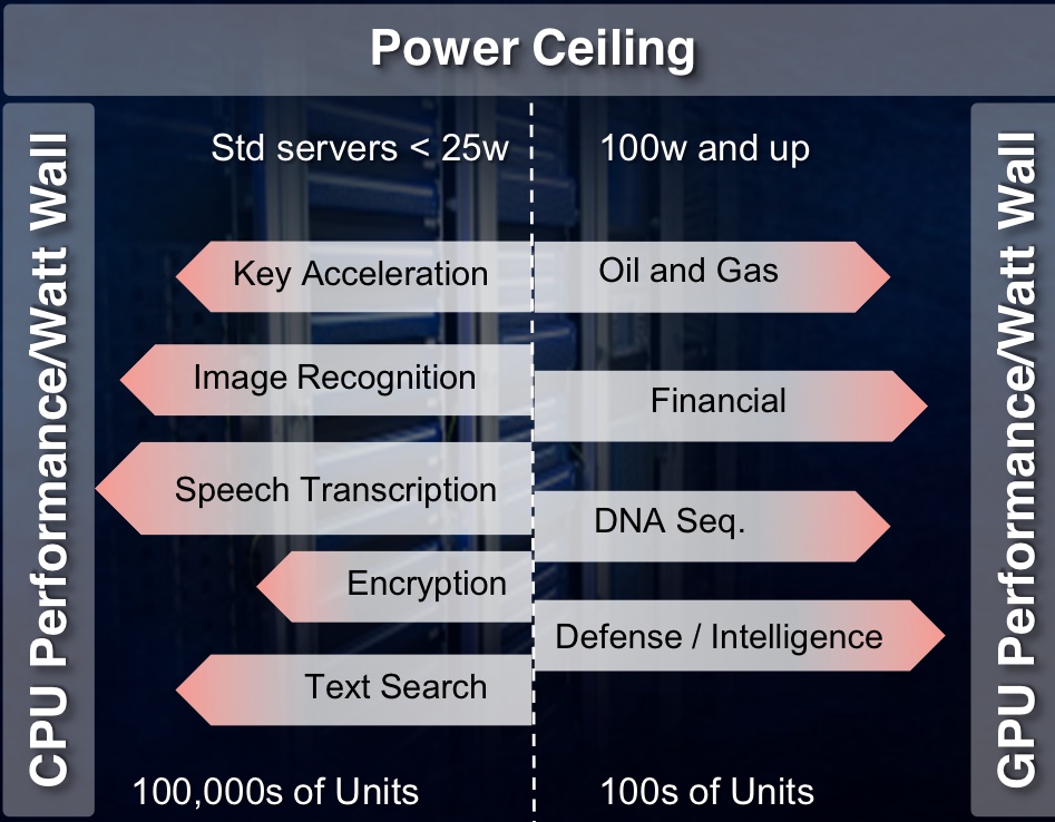 The PCIe accelerator card has a power budget of 25W. Hyper data centres can host hundreds of thousands of servers whereas other industries with more specialist computation requirements use far fewers servers. As such, they can afford a higher power budget per card. Source: Xilinx
Xilinx has developed a software-design environment that simplifies the use of an FPGA as a co-processor alongside the server's x86 instruction set microprocessor.
Dubbed SDAccel, the development environment enables a software engineer to write applications using OpenCL, C or the C++ programming language running on servers in the data centre.
Applications can be developed to run on the server's FPGA-based acceleration card without requiring design input from a hardware designer. Until now, a hardware engineer has been needed to convert the code into the RTL hardware description language that is mapped onto the FPGA's logic gates using synthesis tools.
"[Now with SDAccel] you suffer no degradation in [processing] performance/ Watt compared to hand-crafted RTL on an FPGA," says Giles Peckham, regional americas and EMEA marketing director at Xilinx. "And you move the entire design environment into the software domain; you don't need a hardware designer to create it."
Data centre acceleration
The data centre is the first application targeted for SDAccel along with the accompanying FPGA accelerator cards developed by Xilinx's three hardware partners: Alpha Data, Convey and Pico Computing.
The FPGA cards connect to the server's host processor via the PCI Express (PCIe) interface are not just being aimed at leading internet content providers but also institutions and industries that have custom computational needs. These include oil and gas, financial services, medical and defence companies.
PCIe cards have a power budget of 25W, says Xilinx. The card's power can be extended by adding power cables but considering that hyper data centres can have hundreds of thousands of servers, every extra Watt consumed comes at a cost.
Microsoft has reported that a production pilot it set up that had 1,632 servers using PCIe-based FPGA cards, achieved a doubling of throughput, a 29 percent lower latency, and a 30 percent cost reduction compared to servers without accelerator cards
In contrast, institutions and industries use far fewer servers in their data centres. "They can stomach the higher power consumption, from a cost perspective and in terms of dissipating the heat, up to a point," says Peckham. Their accelerator cards may consume up to 100W. "But both have this limitation because of the power ceiling," he says.
China’s largest search-engine specialist, Baidu, uses neural-network processing to solve problems in speech recognition, image search, and natural language processing, according to The Linley Group senior analyst, Loring Wirbel.
Baidu has developed a 400 Gigaflop software-defined accelerator board that uses a Xilinx Kintex-7 FPGA that plugs into any 1U or 2U high server using PCIe. Baidu says that the FPGA board achieves four times higher performance than graphics processing units (GPUs) and nine times higher performance than CPUs, while consuming between 10-20W.
Microsoft has reported that a production pilot it set up that had 1,632 servers using PCIe-based FPGA cards, achieved a doubling of throughput, a 29 percent lower latency, and a 30 percent cost reduction compared to servers without accelerator cards.
"The FPGA can implement highly parallel applications with the exact hardware required," says Peckham. Since the dynamic power consumed by the FPGA depends on clock frequency and the amount of logic used, the overall power consumption is lower than a CPU or GPU. That is because the FPGA's clock frequency may be 100MHz compared to a CPU's or GPU's 1 GHz, and the FPGA implements algorithms in parallel using hardware tailored to the task.
 FPGA processing performance/ W for data centre acceleration tasks compared to GPUs and CPUs. Note the FPGA's performance/W advantage increases with the number of software threads. Source: Xilinx
SDAccel
To develop a design environment that a software developer alone can use, Xilinx has to make SDAccel aware of the FPGA card's hardware, using what is known as a board support package. "There needs to be an understanding of the memory and communications available to the FPGA processor," says Peckham. "The processor then knows all the hardware around it."
Xilinx claims SDAccel is the industry's first architecturally optimising compiler for FPGAs. "It is as good as hand-coding [RTL]," says Peckham. The tool also delivers a CPU-/ GPU-like design environment. "It is also the first tool that enables designs to have multiple operations at different times on the same FPGA," he says. "You can reconfigure the accelerator card in runtime without powering down the rest of the chip."
SDAccel and the FPGA cards are available, and the tool is with several customers. "We have proven the tool, debugged it, created a GUI as opposed to a command line interface, and have three FPGA boards being sold by our partners," says Peckham. "More partners and more boards will be available in 2015."
Peckham says the simplified design environment appeals to companies not addressing the data centre. "One company in Israel uses a lot of Virtex-6 FPGAs to accelerate functions that start in C code," he says. "They are using FPGAs but the whole design process is drawn-out; they were very happy to learn that [with SDAccel] they don't have to hand-code RTL to program them."
Xilinx is working to extend OpenCL for computing tasks beyond the data centre. "It is still a CPU-PCIe-to-co-processor architecture but for wider applications," says Peckham.
For Part 2, click here
For Part 3, click here
NextIO simplifies top of rack switching with I/O virtualisation
NextIO has developed virtualised input/output (I/O) equipment that simplifies switch design in the data centre.
 "Our box takes a single virtual NIC, virtualises that and shares that out with all the servers in a rack"
John Fruehe, NextIO
The platform, known as vNET, replaces both Fibre Channel and Ethernet top-of-rack switches in the data centre and is suited for use with small one rack unit (1RU) servers. The platform uses PCI Express (PCIe) to implement I/O virtualisation.
"Where we tend to have the best success [with vNET] is with companies deploying a lot of racks - such as managed service providers, service providers and cloud providers - or are going through some sort of IT transition," says John Fruehe, vice president of outbound marketing at NextIO.
Three layers of Ethernet switches are typically used in the data centre. The top-of-rack switches aggregate traffic from server racks and link to end-of-row, aggregator switches that in turn interface to core switches. "These [core switches] aggregate all the traffic from all the mid-tier [switches]," says Fruehe. "What we are tackling is the top-of-rack stuff; we are not touching end-of-row or the core."
A similar hierarchical architecture is used for storage: a top-of-rack Fibre Channel switch, end-of-row aggregation and a core that connects to the storage area network. NextIO's vNET platform also replaces the Fibre Channel top-of-rack switch.
"We are replacing those two top-of-rack switches - Fibre Channel and Ethernet - with a single device that aggregates both traffic types," says Fruehe.
vNET is described by Fruehe as an extension of the server I/O. "All or our connections are PCI Express, we have a simple PCI Express card that sits in the server, and a PCI Express cable," he says. "To the server, it [vNET] looks like a PCI Express hub with a bunch of I/O cards attached to it." The server does not discern that the I/O cards are shared across multiple servers or that they reside in an external box.
For IT networking staff, the box appears as a switch providing 10 Gigabit Ethernet (GbE) ports to the end-of-rack switches, while for storage personnel, the box provides multiple Fibre Channel connections to the end-of-row storage aggregation switch. "Most importantly there is no difference to the software," says Fruehe.

I/O virtualisation
NextIO's technology pools the I/O bandwidth available and splits it to meet the various interface requirements. A server is assigned I/O resources yet it believes it has the resources all to itself. "Our box directs the I/O the same way a hypervisor directs the CPU and memory inside a server for virtualisation," says Fruehe.
There are two NextIO boxes available that support up to 15 or up to 30 servers. One has 30, 10 Gigabit-per-second (Gbps) links and the other 15, 20Gbps links. These are implemented as 30x4 and 15x8 PCIe connections, respectively, that connect directly to the servers.
A customer most likely uses two vNET platforms at the top of the rack, the second being used for redundancy. "If a server is connected to two, you have 20 or 40 Gig of aggregate bandwidth," says Fruehe.
NextIO exploits two PCIe standards known as single root I/O virtualisation (SRIOV) and multi-root I/O virtualisation (MRIOV).
SRIOV allows a server to take an I/O connection like a network card, a Fibre Channel card or a drive controller and share it across multiple server virtual machines. MRIOV extends the concept by allowing an I/O controller to be shared by multiple servers. "Think of SRIOV as being the standard inside the box and MRIOV as the standard that allows multiple servers to share the I/O in our vNET box," says Fruehe.
Each server uses only a single PCIe connection to the vNET with the MRIOV's pooling and sharing happening inside the platform.
 The vNET platform showing the PCIe connections to the servers, the 10GbE interfaces to the network and the 8 Gig Fibre Channel connections to the storage area networks (SANs). Source: NextIO
Meanwhile, vNET's front panel has eight shared slots. These house Ethernet controllers and/or Fibre Channel controllers, and these are shared across the multiple servers.
In affect an application running on the server communicates with its operating system to send the traffic over the PCIe bus to the vNET platform, where it is passed to the relevant network interface controller (NIC) or Fibre Channel card.
The NIC encapsulates the data in Ethernet frames before being sent over the network. The same applies with the host bus adaptor (HBA) that converts the data to be stored to Fibre Channel. "All these things are happening over the PCIe bus natively, and they are handled in different streams," says Fruehe.
In effect, a server takes a single physical NIC and partitions it into multiple virtual NICs for all the virtual machines running on the server. "Our box takes a single virtual NIC, virtualises that and shares that out with all the servers in a rack" says Fruehe. "We are using PCIe as the transport all the way back to the virtual machine and all the way forward to that physical NIC; that is all a PCIe channel."
The result is a high bandwidth, low latency link that is also scalable.
NextIO has a software tool that allows bandwidth to be assigned on the fly. "With vNET, you open up a console and grab a resource and drag it over to a server and in 2-3 seconds you've just provisioned more bandwidth for that server without physically touching anything."
The provisioning is between vNET and the servers. In the case of networking traffic, this is in 10GbE chucks. It is the server's own virtualisation tools that do the partitioning between the various virtual machines.
vNET has an additional four vNET slots - for a total of 12 - for assignment to individual servers. "If you are taking all the I/O cards out of the server, you can use smaller form-factor servers," says Fruehe. But such 1RU servers may not have room for a specific I/O card. Accordingly, the four slots are available to host cards - such as a solid-state drive flash memory or a graphics processing unit accelerator - that may be needed by individual servers.
Operational benefits
There are power and cooling benefits using the vNET platform. First, smaller form factor servers draw less power while using PCIe results in fewer cables and better air flow.
To understand why fewer cables are needed, a typical server uses a quad 1GbE controller and a dual-ported Fibre Channel controller, resulting in six cables. To have a redundant system, a second set of Ethernet and Fibre Channel cards are used, doubling the cables to a dozen. With 30 servers in a rack, the total is 360 cables.
Using NextIO's vNET, in contrast, only two PCIe cables are required per server or 60 cables in total.
On the front panel, there are eight shared slots and these can all be either dual 10GbE port cards or dual 8GbE port Fibre Channel cards or a mix of both. This gives a total of 160GbE or 128 Gig of Fibre Channel. NextIO plans to upgrade the platforms to 40GbE interfaces for an overall capacity of 640GbE.