
Rational and innovative times: JDSU's CTO Q&A Part II

"What happens after 100 Gig is going to be very interesting"
Brandon Collings (right), JDSU
How has JDS Uniphase (JDSU) adapted its R&D following the changes in the optical component industry over the last decade?
JDSU has been a public company for both periods [the optical boom of 1999-2000 and now]. The challenge JDSU faced in those times, when there was a lot of venture capital (VC) money flowing into the system, was that the money was sort of free money for these companies. It created an imbalance in that the money was not tied to revenue which was a challenge for companies like JDSU that ties R&D spend to revenue. You also have much more flexibility [as a start-up] in setting different price points if you are operating on VC terms.
The situation now is very straightforward, rational and predictable.
There is not a huge army of R&D going on. That lack of R&D does not speed up the industry but what it does do is allow those companies doing R&D - and there is still a significant number - a lot of focus and clarity. It also requires a lot of partnership between us, our customers [equipment makers] and operators. The people above us can't just sit back and pick and choose what they like today from myriad start-ups doing all sorts of crazy things.
We very much appreciate this rational time. Visions can be more easily discussed, things are more predictable and everyone is playing from a similar set of rules.
Given the changes at the research labs of system vendor and operators, is there a risk that insufficient R&D is being done, impeding optical networking's progress?
It is hard to say absolutely not as less people doing things can slow things down. But the work those labs did, covered a wide space including outside of telecom.
There is still a sufficient critical mass of research at placed like Alcatel-Lucent Bell Labs, AT&T and BT; there is increasingly work going on in new regions like Asia Pacific, and a lot more in and across Europe. It is also much more focussed - the volume of workers may have decreased but the task still remains in hand.
"There are now design tradeoffs [at speeds higher than 100Gbps] whereas before we went faster for the same distance"
How does JDSU foster innovation and ensure it is focussing on the right areas?
I can't say that we have at JDSU a process that ensures innovation. Innovation is fleeting and mysterious.
We stay very connected to our key customers who are more on the cutting edge. We have very good personal and professional relationships with their key people. We have the same type of relationship with the operators.
I and my team very regularly canvass and have open discussions about what is coming. What does JDSU see? What do you see? What technologies are blossoming? We talk through those sort of things.
That isn't where innovation comes from. But what that can do is sow the seeds for the opportunity for innovation to happen.
We take that information and cycle it through all our technology teams. The guys in the trenches - the material scientists, the free-space optics design guys - we try to educate them with as much of an understanding of the higher-level problems that ultimately their products, or the products they design into, will address.
What we find is that these guys are pretty smart. If you arm them with a wider understanding, you get a much more succinct and powerful innovation than if you try to dictate to a material scientist here is what we need, come back when you are done.
It is a loose approach, there isn't a process, but we have found that the more we educate our keys [key guys] to the wider set of problems and the wider scope of their product segments, the more they understand and the more they can connect their sphere of influence from a technology point of view to a new capability. We grab that and run with it when it makes sense.
It is all about communicating with our customers and understanding the environment and the problem, then spreading that as wide as we can so that the opportunity for innovation is always there. We then nurse it back into our customers.
Turning to technology, you recently announced the integration of a tunable laser into an SFP+, a product you expect to ship in a year. What platforms will want a tunable laser in this smallest pluggable form factor?
The XFP has been on routers and OTN (Optical Transport Network) boxes - anything that has 10 Gig - and those interfaces have been migrated over to SFP+ for compactness and face plate space. There are already packet and OTN devices that use SFP+, and DWDM formats of the SFP+, to do backhaul and metro ring application. The expectation is that while there are more XFP ports today, the next round of equipment will move to SFP+.
Certainly the Ciscos, Junipers and the packet guys are using tunable XFPs in great volume for IP over DWDM and access networks, but the more telecom-centric players riding OTN links or maybe native Ethernet links over their metro rings are probably the larger volume.
What distance can the tunable SFP+ achieve?
The distances will be pretty much the same as the tunable XFP. We produce that in a number of flavours, whether it is metro and long-haul. The initial SFP+ will like be the metro reaches, 80km and things like that.
What is the upper limit of the tunable XFP?
We produce a negative chirp version which can do 80km of uncompensated dispersion, and then we produce a zero chirp which is more indicative of long-haul devices.
In that case the upper limit is more defined by the link engineering and the optical signal-to-noise ratio (OSNR), the extent of the dispersion compensation accuracy and the fibre type. It starts to look and smell like a long-haul lithium niobate transceiver where the distances are limited by link design as much as by the transceiver itself. As for the upper limit, you can push 1000km.
An XFP module can accommodate 3.5W while an SFP+ is about 1.5W. How have you reduced the power to fit the design into an SFP+?
It may be a generation before we get to that MSA level so we are working with our customers to see what level they can tolerate. We'll have to hit a lot less that 3.5W but it is not clear that we have to hit the SFP+ MSA specification. We are already closer now to 1.5W than 3.5W.
"I can't say that we have at JDSU a process that ensures innovation. Innovation is fleeting and mysterious."
Semiconductors now play a key role in high-speed optical transmission. Will semiconductors take over more roles and become a bigger part of what you do?
Coherent transmission [that uses an ASIC incorporating a digital signal processor (DSP)] is not going away. There is a lot of differentiation at the moment in what happens in that DSP, but I think overall it is going to be a tool the system houses use to get the job done.
If you look at 10 Gig, the big advancement there was FEC [forward error correction] and advanced FEC. In 2003 the situation was a lot like it is today: who has the best FEC was something that was touted.
If you look at coherent technology, it is certainly a different animal but it is a similar situation: that is, the big enabler for 40 and 100 Gig. Coherent is advanced technology, enhanced FEC was advanced technology back then, and over time it turned into a standardised, commoditised piece that is central and ubiquitously used for network links.
Coherent has more diversity in what it can do but you'll see some convergence and commoditisation of the technology. It is not going to replace or overtake the importance of photonics. In my mind they play together intimately; you can't replace the functions of photonics with electronics any time soon.
From a JDSU perspective, we have a lot of work to do because the bulk of the cost, the power and the size is still in the photonics components. The ASIC will come down in power, it will follow Moore's Law, but we will still need to work on all that photonics stuff because it is a significant portion of the power consumption and it is still the highest portion of the cost.
JDSU has made acquisitions in the area of parallel optics. Given there is now more industry activity here, why isn't JDSU more involved in this area?
We have been intermittently active in the parallel optics market.
The reality is that it is a fairly fragmented market: there are a lot of applications, each one with its own requirements and customer base. It is tough to spread one platform product around these applications. That said, parallel optics is now a mainstay for 40 and 100 Gig client [interfaces] and we are extremely active in that area: the 4x10, 4x25 and 12x10G [interfaces]. So that other parallel optics capability is finding its way into the telecom transceivers.
We do stay active in the interconnect space but we are more selective in what we get engaged in. Some of the rules there are very different: the critical characteristics for chip interconnect are very different to transceivers, for example. It may be much better to have on-chip optics versus off-chip optics. Obviously that drives completely different technologies so it is a much more cloudy, fragmented space at the moment.
We are very tied into it and are looking for those proper opportunities where we do have the technologies to fit into the application.
How does JDSU view the issues of 200, 400 Gigs and 1 Terabit optical transmission?
What happens after 100 Gig is going to be very interesting.
Several things have happened. We have used up the 50GHz [DWDM] channel, we can't go faster in the 50GHz channel - that is the first barrier we are bumping into.
Second, we're finding there is a challenge to do electronics well beyond 40 Gigabit. You start to get into electronics that have to operate at much higher rates - analogue-to-digital converters, modulator drivers - you get into a whole different class of devices.
Third, we have used all of our tools: we have used FEC, we are using soft-decision FEC and coherent detection. We are bumping into the OSNR problem and we don't have any more tools to run lines rates that have less power to noise yet somehow recover that with some magic technology like FEC at 10 Gig, and soft decision FEC and coherent at 40 and 100 Gig.
This is driving us into a new space where we have to do multi-carrier and bigger channels. It is opening up a lot of flexibility because, well, how wide is that channel? How many carriers do you use? What type of modulation format do you use?
What format you use may dictate the distance you go and inversely the width of the channel. We have all these new knobs to play with and they are all tradeoffs: distance versus spectral efficiency in the C-band. The number of carriers will drive potentially the cost because you have to build parallel devices. There are now design tradeoffs whereas before we went faster for the same distance.
We will be seeing a lot of devices and approaches from us and our customers that provide those tradeoffs flexibly so the carriers can do the best they can with what mother nature will allow at this point.
That means transponders that do four carriers: two of them do 200 Gig nicely packed together but they only achieve a few hundred kilometers, but a couple of other carriers right next door go a lot further but they are a little bit wider so that density versus reach tradeoff is in play. That is what is going to be necessary to get the best of what we can do with the technology.
That is the transmission side, the transport side - the ROADMS and amplifiers - they have to accommodate this quirky new formats and reach requirements.
We need to get amplifiers to get the noise down. So this is introducing new concepts like Raman and flex[ible] spectrum to get the best we can do with these really challenging requirements like trying to get the most reach with the greatest spectral efficiency.
How do you keep abreast of all these subject areas besides conversations with customers?
It is a challenge, there aren't many companies in this space that are broader than JDSU's optical comms portfolio.
We do have a team and the team has its area of focus, whether it is ROADMs, modulators, transmission gear or optical amplifiers. We segment it that way but it is a loose segmentation so we don't lose ideas crossing boundaries. We try to deal with the breadth that way.
Beyond that, it is about staying connected with the right people at the customer level, having personal relationships so that you can have open discussions.
And then it is knowing your own organisation, knowing who to pull into a nebulous situation that can engage the customer, think on their feet and whiteboard there and then rather than [bringing in] intelligent people that tend to require more of a recipe to do what they are doing.
It is all about how to get the most from each team member and creating those situations where the right things can happen.
For Part I of the Q&A, click here
How ClariPhy aims to win over the system vendors

“We can build 200 million logic gate designs”
Reza Norouzian, ClariPhy
ClariPhy is in the camp that believes that the 100 Gigabit-per-second (Gbps) market is developing faster than people first thought. “What that means is that instead of it [100Gbps] being deployed in large volumes in 2015, it might be 2014,” says Reza Norouzian, vice president of worldwide sales and business development at ClariPhy.
Yet the fabless chip company is also glad it offers a 40Gbps coherent IC as this market continues to ramp while 100Gbps matures and overcomes hurdles common to new technology: The 100Gbps industry has yet to develop a cost-effective solution or a stable component supply that will scale with demand.
Another challenge facing the industry is reducing the power consumption of 100Gbps systems, says Norouzian. The need to remove the heat from a 100Gbp design - the ASIC and other components - is limiting the equipment port density achievable. “If you require three slots to do 100 Gig - whereas before you could use these slots to do 20 or 30, 10 Gig lines - you are not achieving the density and economies of scale hoped for,” says Norouzian.
40G and 100G coherent ASICs
ClariPhy has chosen a 40nm CMOS process to implement its 40Gbps coherent chip, the CL4010. But it has since decided to adopt 28nm CMOS for its 100Gbps design – the CL10010 - to integrate features such as soft-decision forward error correction (see New Electronics' article on SD-FEC) and reduce the chip’s power dissipation.
The CL4010 integrates analogue-to-digital and digital-to-analogue converters, a digital signal processor (DSP) and a multiplexer/ demultiplexer on-chip. “Normally the mux is a separate chip and we have integrated that,” says Norouzian.
The first CL4010 samples were delivered to select customers three months ago and the company expects volume production to start by the end of September. The CL4010 also interoperates with Cortina Systems’ optical transport network (OTN) processor family of devices, says the company.
The start-up claims there is strong demand for the CL4010. “When we ask them [operators]: ‘With all the hoopla about 100 Gig, why are you buying all this 40 Gig?’, the answer is that it is a pragmatic solution and one they can ship today,” says Norouzian.
ClariPhy expects 40Gbps volumes to continue to ramp for the next three or four years, partly because of the current high power consumption of 100Gbps. The company says several system vendors are using the CL4010 in addition to optical module customers.
The 28nm 100Gbps CL10010 is a 100 million gate ASIC. ClariPhy acknowledges it will not be first to market with an 100Gbps ASIC but that by using the latest CMOS process it will be well position once volume deployments start from 2014.
ClariPhy is already producing a quad-10Gbps chip implementing the maximum likelihood sequence estimation (MLSE) algorithm used for dispersion compensation in enterprise applications. The device covers links up to 80km (10GBASE-ZR) but the main focus is for 10GBASE-LRM (220m+) applications. “Line cards that used to have four times 10Gbps lanes now are moving to 24 and will use six of these chips,” says Norouzian. The device sits on the card and interfaces with SFP+ or Quad-SFP optical modules.
“The CL10010 is the platform to demonstrate all that we can do but some customers [with IP] will get their own derivatives”
System vendor design wins
The 100Gbps transmission ASIC market may be in its infancy but the market is already highly competitive with clear supply lines to the system vendors.
Several leading system vendors have decided to develop their own ASICs. Alcatel-Lucent, Ciena, Cisco Systems (with the acquisition of CoreOptics), Huawei and Infinera all have in-house 100Gbps ASIC designs.
System vendors have justified the high development cost of the ASIC to get a time-to-market advantage rather than wait for 100Gbps optical modules to become available. Norouzian also says such internally-developed 100Gbps line card designs deliver a higher 100Gbps port density when compared to a module-based card.
Alternatively, system vendors can wait for 100Gbps optical modules to become available from the likes of an Oclaro or an Opnext. Such modules may include merchant silicon from the likes of a ClariPhy or may be internally developed, as with Opnext.
System vendors may also buy 100Gbps merchant silicon directly for their own 100Gbps line card designs. Several merchant chip vendors are targeting the coherent marketplace in addition to ClariPhy. These include such players as MultiPhy and PMC-Sierra while other firms are known to be developing silicon.
Given such merchant IC competition and the fact that leading system vendors have in-house designs, is the 100Gbps opportunity already limited for ClariPhy?
Norouzian's response is that the company, unlike its competitors, has already supplied 40Gbps coherent chips, proving the company’s mixed signal and DSP expertise. The CL10010 chip is also the first publicly announced 28nm design, he says: “Our standard product will leapfrog first generation and maybe even second generation [100Gbps] system vendor designs.”
The equipment makers' management will have to decide whether to fund the development of their own second-generation ASICs or consider using ClariPhy’s 28nm design.
ClariPhy acknowledges that leading system vendors have their own core 100Gbps intellectual property (IP) and so offers vendors a design service to develop their own custom systems-on-chip. For example a system vendor could use ClariPhy's design but replace the DSP core with the system vendor’s own hardware block and software.
 Source: ClariPhy Communications
Norouzian says system vendors making 100Gbps ASICs develop their own intellectual property (IP) blocks and algorithms and use companies like IBM or Fujitsu to make the design. ClariPhy offers a similar service while also being able to offer its own 100Gbps IP as required. “The CL10010 is the platform to demonstrate all that we can do,” says Norouzian. “But some customers [with IP] will get their own derivatives.”
The firm has already made such custom coherent devices using customers’ IP but will not say whether these were 40 or 100Gbps designs.
Market view
ClariPhy claims operator interest in 40Gbps coherent is not so much because of its superior reach but its flexibility when deployed in networks alongside existing 10Gbps wavelengths. “You don't have to worry about [dispersion] compensation along routes,” says Norouzian, adding that coherent technology simplifies deployments in the metro as well as regional links.
And while ClariPhy’s focus is on coherent systems, the company agrees with other 100Gbps chip specialists such as MultiPhy for the need for 100Gbps direct-detect solutions for distances beyond 40km. “It is very likely that we will do something like that if the market demand was there,” says Norouzian. But for now ClariPhy views mid-range 100Gbps applications as a niche opportunity.
Funding
ClariPhy raised US $14 million in June. The biggest investor in this latest round was Nokia Siemens Networks (NSN).
An NSN spokesperson says working with ClariPhy will help the system vendor develop technology beyond 100Gbps. “It also gives us a clear competitive edge in the optical network markets, because ClariPhy’s coherent IC and technology portfolio will enable us to offer differentiated and scalable products,” says the spokesperson.
The funding follows a previous round of $24 million in May 2010 where the investors included Oclaro. ClariPhy has a long working relationship with the optical components company that started with Bookham, which formed Oclaro after it merged with Avanex.
“At 100Gbps, Oclaro get some amount of exclusivity as a module supplier but there is another module supplier that also gets access to this solution,” says Norouzian. This second module supplier has worked with ClariPhy in developing the design.
ClariPhy will also supply the CL10010 to the system vendors. “There are no limitations for us to work with OEMs,” he says.
The latest investment will be used to fund the company's R&D effort in 100, 200 and 400Gbps, and getting the CL4010 to production.
Beyond 100 Gig
The challenge at higher data rates that 100Gbps is implementing ultra-large ASICs: closing the timings and laying out vast digital circuitry. This is an area the company has been investing in over the last 18 months. “Now we can build 200 million logic gate designs,” says Norouzian.
Moving from 100Gbps to 200Gbps wavelengths will require higher order modulation, says Norouzian, and this is within the realm of its ASIC.
Going to 400Gbps will require using two devices in parallel. One Terabit transmission however will be far harder. “Going to one Terabit requires a whole new decade of development,” he says.
Further reading:
Optical networking market in rude health
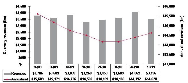 Quarterly market revenues, global optical networking (1Q 2011). Source: Ovum
Despite recent falls in optical equipment makers’ stock, the optical networking market remains in good health with analysts predicting 6-7% growth in 2011.
For Andrew Schmitt, directing analyst for optical at Infonetics Research, unfulfilled expectations are nothing new. Optical networking is a market of single-digit yearly growth yet in the last year certain market segments have grown above average: spending on ROADM-based wavelength division multiplexing (WDM) optical network equipment, for example, has grown 20% since the first quarter of 2010.
“Every few years people get this expectation that there is going to be this hockey stick [growth] and it is not,” says Schmitt. “There has been a lot of Wall Street money moving into this sector in the latter part of 2010 and first part of this year and they have just had their expectations reset, but operationally the industry is very healthy.”

“Nothing in this business changes quickly but the pace of change is starting to accelerate”
Andrew Schmitt, Infonetics Research
But Schmitt acknowledges that there is industry concern about the market outlook. “There have been lots of client calls in the first half of the year wanting to talk numbers,” says Schmitt. “When the market is growing rapidly there is no need for such calls but when it is uncertain, customers put more time into understanding what is going on.”
Both Infonetics and market research firm Ovum say the optical networking market grew 7% globally in the last year (2Q10 to 1Q11).
Ovum says the market reached US $3.5bn in the first quarter of 2011 and it expects 6% growth this year. “Most of the growth will come from North America—general recovery, stimulus-related spending, and LTE (Long Term Evolution)-inspired spending; and from South and Central America mostly mobile and fixed broadband-related,” says Dana Cooperson, network infrastructure practice leader at Ovum.
Ovum also notes that optical networking annualised spending for the last four quarters (2Q10-1Q11) finally went into the black with 1% growth, to reach $14.6bn. Annualised share figures are a strong indicator of longer-term market trends, says Ovum.
Market growth
Factors accounting for the growth include optical equipment demand for mobile and broadband backhaul. Carriers are also embarking on a multi-year optical upgrade to 40 and 100 Gigabit transmission over Optical Transport Network (OTN) and ROADM-based networks. Infonetics notes that ROADM spending in particular set a new high in the first quarter, rising 4% sequentially.
Ovum expects overall growth to come from metro and backbone WDM markets and from LTE. “For metro it is a combination of new builds, as DWDM continues to take over the metro core from SONET/SDH, and expansions of ROADM and 40 Gigabit,” says Cooperson. “For backbone it is a combination of retrofits for 40 and 100 Gigabit and overbuilds with 40 and 100 Gigabit coherent-optimised systems.”
Many operators are also looking at OTN switching and how it can help with network efficiency and manageability, she says, while mobile backhaul continues to be a hot spot as well at the access end of the network.
The Americas are the regions accounting for market growth whereas in Asia-Pacific and Europe, Middle East and Africa the spending remains flat.
“We’re not as bullish on Europe as I’ve heard some others are,” says Cooperson. “We expected China to slow down as capital intensities in the 34-35% seen in 2008 and 2009 were unsustainable. We saw the cooling down a bit earlier in 2010 than we had expected, but it did cool down and will continue to.”
Ovum expects Asia-Pacific as a whole to be moribund. But at least the pullbacks in China will be countered by slow growth in Japan and a big upsurge in India after a huge decline last year due to delayed 3G-related builds among other issues.
Outlook
Ovum is optimistic about the optical networking market due to continued competitive pressures and traffic growth. “We don’t think traffic growth can just continue without attention to the underlying issues related to revenue pressure, regardless of competitive pressures,” says Cooperson. “But newer optical and packet systems offer significant improvements over the old in terms of power efficiency, manageability, and of course 40 and 100 Gigabit coherent and ROADM features.”
“Most of the growth will come from North America"
Dana Cooperson, Ovum.
Many networks worldwide are also due for a core infrastructure update to benefit capacity and efficiency while many other operators are upgrading their access networks for mobile backhaul and enterprise Ethernet services.
Schmitt stresses that while it is right to talk about a 'core reboot', there are all sorts of operators that make up the market: the established carriers, those focussed on Layer 2 and Layer 3 transport, dark fibre companies and cable companies.
“Everyone has a different business so there is not a whole lot of group-think in this industry,” says Schmitt. “So when you talk about a transition to 40 and 100 Gigabit, some carriers will make that transition earlier than others because the nature of their business demands it.”
However, there are developments in equipment costs that are leading to change. “Once you get out to 2013-14, 100 Gigabit [transport] looks really good relative to 40 Gigabit and tunable XFPs at 10 Gigabit look really, really good,” says Schmitt, who believes these are going to be two dominating technologies. “People are going to use 100 Gigabit and when they can afford to throw more 10 Gigabit at the [capacity] problem, in shorter metro and regional spans, they will use tunable XFPs,” he says. “That is a whole new level in terms of driving down cost at 10 Gigabit that people haven’t factored in yet.”
Pacier change
The move to 100 Gigabit will not lead to increased spending, stresses Schmitt. Rather its significance is as a ‘mix shift’: The adoption of 100 Gigabit will shift spending from older systems to newer ones so that the technology is interesting in terms of market share shift rather than by growing overall revenues.
That said, there are areas of optical spending where capital expenditure (capex) is growing faster than the single-digit trend. These include certain competitive telco providers and dark fibre providers like AboveNet, TimeWarner Telecom and Colt. “You look at their capex year-over-year and it is increasing in some cases more over 20% a year,” says Schmitt.
He also notes that while the likes of Google, Yahoo, Microsoft and Apple do not spend on optical equipment as much as established operators such as Verizon or AT&T, their growth rate is higher. “There are sectors of the market that are growing quickly, and competition that are positioned to service those sectors successfully are going to see above-trend growth,” says Schmitt.
He highlights three areas of innovations - ‘big vectors’- that are going to change the business.
One is optical transport's move away from simple on-off keying signalling that opens up all kinds of innovation. Another is the shift in the players buying optical equipment. “A lot more of the R&D is driven by the AboveNets, Time Warners, Comcasts and the Googles and less by the old time PTTs,” says Schmitt. “That is going to change the way R&D is done.”
The third is photonic integration which Schmitt equates to the very early state of the electronics business. While Infinera has done some interesting things with integration, its latest 500 Gigabit PIC (photonic integrated circuit) is a big leap in density, he says: “It will be interesting if that sort of technology crosses over into other applications such as short- and intermediate-reach applications.”
“Nothing in this business changes quickly but the pace of change is starting to accelerate,” says Schmitt. “These three things, when you throw them together in a pot, are going to result in some unpredictable outcomes.”
OTN hardware gets the 100 Gigabit treatment
 “The real market demand is for simple systems - the transponder and interfaces to the routers"
Lars Pedersen, AppliedMicro
Why is this significant?
The OTN standard, defined by the telecom standards body of the International Telecommunication Union (ITU-T), has existed for a decade but has emerged recently as a key networking technology.
“SONET/SDH is now legacy while packet optical is next-generation work,” says Sterling Perrin, senior analyst at Heavy Reading. “OTN has emerged as an interim step away from SONET/SDH that is able to handle packets.”
With the advent of 100 Gigabit-per-second (Gbps) optical transmission, OTN has been upgraded to handle 100Gbps signals and multiplex existing 10Gbps and 40Gbps OTN within the 100 Gigabit framing format. AppliedMicro claims to be first-to-market with merchant 100Gbps OTN hardware.
AppliedMicro’s 100Gbps OTN designs are implemented using field-programmable gate arrays (FPGAs) and will become available to system vendors this quarter. Using FPGAs allows vendors to start their hardware designs early, adding AppliedMicro’s FPGA software as the OTN design is completed.
What has been done?
The TPOT414 and TPOT424 designs, implemented on a line card, perform mapping - taking a 100 Gigabit client-side signal and turning into a 100Gbps line-side signal for transmission - and regeneration of a 100Gbps signal.
The 100Gbps OTN muxponder uses framing and mapping but adds multiplexing between 10, 40 Gbps and 100Gbps streams. One application is a router taking IP traffic at different rates and framing them before transmission over a 100Gbps dense wavelength division multiplexing (DWDM) network.
The 100Gbps muxponder comprises AppliedMicro’s PQ60 framer/mapper chip and multiplexing FPGA products, referred to by AppliedMicro as soft silicon. “It [soft silicon] is a combination of an FPGA and the programming image delivered as one unified component,” says Lars Pedersen, TPACK’s CTO. “There is still some uncertainty as to the specification and what is needed.”
The benefits of a soft silicon approach compared to an application-specific standard product (ASSP) include the ability to reprogram the design to accommodate standards’ changes, and allowing system vendors to add new elements as they customise their designs.
AppliedMicro also provides an application programming interface (API) which simplifies control and maintenance when several of its designs are combined to implement a more complex function. “From a software perspective it looks like one combined function,” says Pedersen. The 100Gbps muxponder, for example, is controlled via the API. The API also allows software reuse were AppliedMicro to offer the functions as an ASSP chip.
The TPOT OTN architecture
The two functions – the TPOT414 and TPOT424 – are implemented on a common FPGA design.
 The TPOT414: Source: AppliedMicro
The TPOT414 has a 100 Gigabit Ethernet (GbE) CAUI interface (10 x 11.2Gbps) and performs physical coding sub-layer (PCS) monitoring per lane before mapping the signal into OTU4, prior to long-haul transmission. The two signals - the 100GbE and the 100Gbps line side - have separate clocks and the role of the mapper is to place the 100GbE stream into the OTN format.
The TPOT414 could be used to interface two optical modules on a line card: a CFP module that takes in a 100GbE client signal and an MSA-168 long-haul transponder whose electrical input is the OTN OTU4 signal.
 The TPOT424 Source: AppliedMicro
The second design, the TPOT424, takes in an OTU4 signal made up of a payload and overhead components. The overhead part that includes a forward error correction (FEC) is terminated - errors corrected and signal measurements made – before the payload is put into a new OTU4 frame and a fresh overhead including a new FEC scheme is applied.
Both the TPOT414 and TPOT424 use standard FEC from the ITU-T G.709 standard. Separate devices in the optical module are needed if more powerful FECs are used. AppliedMicro says it will support more powerful FECs in future 100Gbps OTN devices.
“These [the TPOT414 and TPOT424] are the bulk of the emerging market and are the most needed components to start with,” says Pedersen.
The 100G OTN muxponder also supports the multiplexing function, including support for 10GbE and 40GbE, OC-192 and OC-768 SONET/SDH, and 8Gbps and 10Gbps Fibre Channel signals
What next?
Pedersen says there is now significant demand for its 100Gbps OTN designs as vendors prepare to launch systems supporting 100Gbps interfaces in 2011 and 2012. These include packet optical transport platforms and 100Gbps IP router line cards.
“The real market demand is for simple systems - the transponder and interfaces to the routers,” says Pedersen. “But at the same time there are many vendors working on packet optical transport platforms.”
The company does not rule out developing ASSP designs that support100Gbps OTN.