
Open ROADM gets deployed as work starts on Release 6.0
AT&T has deployed Open ROADM technology in its network and says all future reconfigurable optical add-drop multiplexer (ROADM) deployments will be based on the standard.
“At this point, it is in a single metro and we are working on a second large metro area,” says John Paggi, assistant vice president member of technical staff, network infrastructure and services at AT&T.
Open ROADM listed as a requirement in RFPs (Request For Proposals) from many other service providers
As shown are the various elements included in the disaggregated Open ROADM MSA. Also shown is the hierarchical SDN controller architecture with the federated controllers overseeing the optical layer and the multi-layer controller overseeing the path creation across the layer, from IP to optical. Source: Open ROADM MSA
Meanwhile, the Open ROADM multi-source agreement (MSA) continues to progress, with members working on Release 6.0 of the standard.
Motivation
AT&T is a founding member of the Open ROADM MSA along with system vendors Ciena, Fujitsu and Nokia. The organisation has since grown to 23 members, 13 of which operate networks. Besides AT&T, the communications service providers include Deutsche Telekom, Orange, KDDI, SK Telecom and Telecom Italia.
The initiative was created to promote a disaggregated ROADM standard that enables interoperability between vendors’ ROADMs.
The specification work includes the development of open interfaces to control the ROADMs using software-defined networking (SDN) technology. The scope of the disaggregated design has also been expanded beyond ROADMs to include optical transceivers, OTN switching to handle sub-wavelength traffic, and optical amplifiers.
AT&T viewed the MSA as a way to change the traditional model of assigning two ROADM system vendors for each of its metro regions.
“We had two suppliers to keep each other honest,” says Paggi. “But once we had committed a region to a supplier, we were more or less beholden to that supplier for additional ROADM and transponder purchases.”
AT&T wanted ‘true hyper-competition’ among ROADM and transponder suppliers and the Open ROADM MSA was the result.
The operator saw the MSA as a way to reduce costs and speed up innovation by using an open networking model. Opening up and standardising the design would also allow innovative start-up vendors to participate. With the traditional supply model, an operator would favour larger firms knowing it would be dependent on the suppliers for 5-10 years.
“Because you can mix and match different suppliers, Open ROADM allows us to introduce disrupters to our environment,” says Paggi.
Evolution
The first Open ROADM revision used 100-gigabit wavelengths and a 50GHz fixed grid. A flexible grid and in-line amplification that extended the reach of 100-gigabit wavelengths to 1,000km were then added with Revision 2.
“In Revision 3 we made Open ROADM applicable to more use cases,” says Martin Birk, director member of technical staff, network infrastructure and services, AT&T. “We started introducing things like OTUCn and FlexO in preparation for 400 gigabits.” The OTN ‘Beyond 100 gigabit’ OTUCn format comprises ‘n’ multiples of 100-gigabit OTUC frames, while FlexO refers to the Flexible OTN format.
Adopting OTN technologies is part of enabling Open ROADM to support 200-, 300- and 400-gigabit wavelengths.
Revision 4 then added ODUFlex, 400-gigabit clients, and support for low-noise amplifiers to further extend reach, while the latest fifth revision adds streaming telemetry for network monitoring using work from the OpenConfig industry group.
“A lot of features that widen considerably the application of Open ROADM,” says Birk.
Revision 6.0
The frequency of each Open ROADM release was initially once a year but now the scope of each revision has been curtailed to enable two releases a year. Members are polled as to what new features are required at the start of each standardisation process.
Now, the MSA members are working on revision 6.0 that covers ‘all directions’ of the standard.
“We are improving the control plane interoperability with more features,” says Birk. “Right now you have a single network view; in future, you could have an idealised network plan and a network view with actual failures, and you could provision services across these network views.”
And with the advent of 600-gigabit, 800-gigabit and even 1.2-terabit coherent wavelengths, OpenROADM members may add support for faster speeds than 400 gigabits.
“Just as our suppliers continue to evolve their roadmaps, so does the Open ROADM MSA to stay relevant,” says Birk.
AT&T’s Open ROADM deployments support 100-gigabit wavelengths while the 400-gigabit technology is still in development.
“The ROADMs will not change; the only thing that will change is the software,” says Birk. “And in a disaggregated design, you can leave the ROADMs on version 2.0 and upgrade the transponders to 400 gigabits and version 5.0.”
This, says Birk, is why it is much easier to introduce new technology with an open design compared to monolithic platforms where an upgrade involves all the element management systems, ROADMs and transponders.
Status
The Open ROADM MSA says it is up to individual network operator members to declare the status of their Open ROADM network deployments. Accordingly, the status of overall Open ROADM deployments is unclear.
What AT&T will say is that it is being approached by vendors that want to demonstrate their Open ROADM technology to the operator.
“When we ask them why they have done this without any agreement that AT&T would purchase their solutions, they respond that they are seeing Open ROADM listed as a requirement in RFPs (Request For Proposals) from many other service providers,” says Paggi. “They have taken it upon themselves to develop Open ROADM-compliant products.”
At the OFC show earlier this year, an Open ROADM MSA showcased an SDN controller turning up a wavelength to send virtual machines between two data centres. The SDN controller then terminated the optical connection on completion of the transfer.
Operators AT&T and Orange were part of the demonstration as was the University of Texas, Dallas. “They [the University of Texas] are a supercomputing centre and they can create some nice applications on top of Open ROADM,” says Birk.
The system vendors involved in the OFC demonstration included Ciena, Fujitsu, ECI Telecom, Infinera and Juniper Networks.

FPGAs with 56-gigabit transceivers set for 2017
The company demonstrated a 56-gigabit transceiver using 4-level pulse-amplitude modulation (PAM-4) at the recent OFC show. The 56-gigabit transceiver, also referred to as a serialiser-deserialiser (serdes), was shown successfully working over backplane specified for 25-gigabit signalling only.
 Gilles GarciaXilinx's 56-gigabit serdes is implemented using a 16nm CMOS process node but the first FPGAs featuring the design will be made using a 7nm process. Gilles Garcia says the choice of 7nm CMOS is solely a business decision and not a technical one.
”Optical module [makers] will take another year to make something decent using PAM-4," says Garcia, Xilinx's director marketing and business development, wired communications. "Our 7nm FPGAs will follow very soon afterwards.”
The company is still to detail its next-generation FPGA family but says that it will include an FPGA capable of supporting 1.6 terabit of Optical Transport Network (OTN) using 56-gigabit serdes only. At first glance that implies at least 28 PAM-4 transceivers on a chip but OTN is a complex design that is logic not I/O limited suggesting that the FPGA will feature more than 28, 56-gigabit serdes.
Applications
Xilinx’s Virtex UltraScale and its latest UltraScale+ FPGA families feature 16-gigabit and 25-gigabit transceivers. Managing power consumption and maximising reach of the high-speed serdes are key challenges for its design engineers. Xilinx says it has 150 engineers for serdes design.
“Power is always a key challenge because as soon as you talk about 400-gigabit to 1-terabit per line card, you need to be cautious about the power your serdes will use,” says Garcia. He says the serdes need to adapt to the quality of the traces for backplane applications. Customers want serdes that will support 25 gigabit on existing 10-gigabit backplane equipment.
Xilinx describes its Virtex UltraScale as a 400-gigabit capable single-chip system supporting up to 104 serdes: 52 at 16 gigabit and 52 at 25 gigabit.
The UltraScale+ is rated as a 500-gigabit to 600-gigabit capable system, depending on the application. For example, the FPGA could support three, 200-gigabit OTN wavelengths, says Garcia.
Xilinx says the UltraScale+ reduces power consumption by 35% to 50% compared to the same designs implemented on the UltrasScale. The Virtex UltraScale+ devices also feature dedicated hardware to implement RS-FEC, freeing up programmable logic for other uses. RS-FEC is used with multi-mode fibre or copper interconnects for error correction, says Xilinx. Six UltraScale+ FPGAs are available and the VU13P, not yet out, will feature up to 128 serdes, each capable of up to 32 gigabit.
We don’t need retimers so customers can connect directly to the backplane at 25 gigabit, thereby saving space, power and cost
The UltraScale and UltraScale+ FPGAs are being used in several telecom and datacom applications.
For telecom, 500-gigabit and 1-terabit OTN designs are an important market for the UltraScale FPGAs. Another use for the FPGA serdes is for backplane applications. “We don’t need retimers so customers can connect directly to the backplane at 25 gigabit, thereby saving space, power and cost,” says Garcia. Such backplane uses include OTN platforms and data centre interconnect systems.
The FPGA family’s 16-gigabit serdes are also being used in 10-gigabit PON and NG-PON2 systems. “When you have an 8-port or 16-port system, you need to have a dense serdes capability to drive the [PON optical line terminal’s] uplink,” says Garcia.
For data centre applications, the FPGAs are being employed in disaggregated storage systems that involved pooled storage devices. The result is many 16-gigabit and 25-gigabit streams accessing the storage while the links to the data centre and its servers are served using 100-gigabit links. The FPGA serdes are used to translate between the two domains (see diagram).
 Source: Xilinx
For its next-generation 7nm FPGAs with 56-gigabit transceivers, Xilinx is already seeing demand for several applications.
Data centre uses include server-to-top-of-rack links as the large Internet providers look move from 25 gigabit to 50- and 100-gigabit links. Another application is to connect adjacent buildings that make up a mega data centre which can involve hundreds of 100-gigabit links. A third application is meeting the growing demands of disaggregated storage.
For telecom, the interest is being able to connect directly to new optical modules over 50-gigabit lanes, without the need for gearbox ICs.
Optical FPGAs
Altera, now part of Intel, developed an optical FPGA demonstrator that used co-packaged VCSELs for off-chip optical links. Since then Altera announced its Stratix 10 FPGAs that include connectivity tiles - transceiver logic co-packaged and linked with the FPGA using interposer technology.
Xilinx says it has studied the issue of optical I/O and that there is no technical reason why it can’t be done. But the issue is a business one when integrating optics in an FPGA, he says: “Who is responsible for the yield? For the support?”
Garcia admits Xilinx could develop its own I/O designs using silicon photonics and then it would be responsible for the logic and the optics. “But this is not where we are seeing the business growing,” he says.
Altera’s 30 billion transistor FPGA
- The Stratix 10 features a routing architecture that doubles overall clock speed and core performance
- The programmable family supports the co-packaging of transceiver chips to enable custom FPGAs
- The Stratix 10 family supports up to 5.5 million logic elements
- Enhanced security features stop designs from being copied or tampered with
Altera has detailed its most powerful FPGA family to date. Two variants of the Stratix 10 family have been announced: 10 FPGAs and 10 system-on-chip (SoC) devices that include a quad-core 64-bit architecture Cortex-A53 ARM processor alongside the programmable logic. The ARM processor can be clocked at up to 1.5 GHz.
The Stratix 10 family is implemented using Intel’s 14nm FinFET process and supports up to 5.5 million logic elements. The largest device in Altera’s 20nm Arria family of FPGAs has 1.15 million logic elements, equating to 6.4 billion transistors. “Extrapolating, this gives a figure of some 30 billion transistors for the Stratix 10,” says Craig Davis, senior product marketing manager at Altera.
 Altera's HyperFlex routing architecture. Shown (pointed to by the blue arrow) are the HyperFlex registers that sit at the junction of the interconnect traces. Also shown are the adaptive logic module blocks. Source: Altera.
The FPGA family uses a routing fabric, dubbed HyperFlex, to connect the logic blocks. HyperFlex is claimed to double the clock speed compared to designs implemented using Altera’s Stratix V devices, to achieve gigahertz rates. “Having that high level of performance allows us to get to 400 gigabit and one terabit OTN (Optical Transport Network) systems,” says Davies.
The FPGA company detailed the Stratix 10 a week after Intel announced its intention to acquire Altera for US $16.7 billion.
Altera is also introducing with the FPGA family what it refers to as heterogeneous 3D system packaging and integration. The technology enables a designer to customise the FPGA’s transceivers by co-packaging separate transceiver integrated circuits (ICs) alongside the FPGA.
Different line-rate transceivers can be supported to meet a design's requirements: 10, 28 or 56 gigabit-per-second (Gbps), for example. It also allows different protocols such as PCI Express (PCIe), and different modulation formats including optical interfaces. Altera has already demonstrated a prototype FPGA co-packaged with optical interfaces, while Intel is developing silicon photonics technology.
HyperFlex routing
The maximum speed an FPGA design can be clocked is determined by the speed of its logic and the time it takes to move data from one part of the chip to another. Increasingly, it is the routing fabric rather than the logic itself that dictates the total delay, says Davis.
This has led the designers of the Stratix 10 to develop the HyperFlex architecture that adds a register at each junction of the lines interconnecting the logic elements.
Altera first tackled routing delay a decade ago by redesigning the FPGA’s logic building block. Altera went from a 4-input look-up table logic building block to a more powerful 8-input one that includes output registers. Using the more complex logic element - the adaptive logic module (ALM) - simplifies the overall routing. “You are essentially removing one layer of routing from your system,” says Davies.
When an FPGA is programmed, the file is presented that dictates how the wires and hence the device’s logic are connected. The refinement with HyperFlex is that there are now registers at those locations where the switching between the traces occurs. A register can either be bypassed or used.
“It allows us to put the registers anywhere in the design, essentially placing them in an optimum place for a given route across the FPGA,” says Davies. The number of hyper-registers in the device's routing outnumber the standard registers in the ALM blocks by a factor of ten.
Using the registers, designers can introduce data pipelining to reduce overall delay and it is this pipelining, combined with the advanced 14nm CMOS process, that allows a design to run at gigahertz rates.
“We have made the registers small but they add one or two percent to the total die area, but in return it gives us the ability to go to twice the performance,” says Davies. “That is a good trade-off.
The biggest change getting HyperFlex to work has been with the software tools, says Davies. HyperFlex and the associated tools has taken over three years to develop.
“This is a fundamental change,” says Davies. “It [HyperFlex] is relatively simple but it is key; and it is this that allows customers to get to this doubling of core performance.”
The examples cited by Altera certainly suggest significant improvements in speed, density, power dissipation, but I want to see that in real-world designs
Loring Wirbel, The Linley Group
Applications
Altera says that over 100 customer designs have now been processed using the Stratix 10 development tools.
It cites as an example a current 400 gigabit design implemented using a Stratix V FPGA that requires a bus 1024-bits wide, clocked at 390MHz. The wide bus consumes considerable chip area and routing it to avoid congestion is non-trivial.
Porting the design to a Stratix 10 enables the bus to be clocked at 781MHz such that the bus width can be halved to 512 bits. “It reduces congestion, makes it easier to do timing closure and ship the design,” says Davies. “This is why we think Stratix 10 is so important for high-performance applications like OTN and data centres.” Timing closure refers to the tricky part of a design where the engineer may have to iterate to ensure that a design meets all the timing requirements.
For another, data centre design, a Stratix 10 device can replace five Stratix V ICs on one card. The five FPGAs are clocked at 250MHz, run PCIe Gen2 x8 interfaces and DDR3 x72 memory clocked at 800MHz. Overall the power consumed is 120W. Using one Stratix 10 chip clocked at 500MHz, faster PCIe Gen3 x8 can be supported as can a wider DDR3 x144 memory clocked at 1.2GHz, with only 44W consumed.
Loring Wirbel, senior analyst at The Linley Group, says that Altera’s insertion of pipelined registers to cut average trace lengths is unique.
“The more important question is, can the hyper-register topology regularly gain the type of advantages claimed?” says Wirbel. “The examples cited by Altera certainly suggest significant improvements in speed, density, power dissipation, but I want to see that in real-world designs.”
We are also looking at optical transceivers directly connected to the FPGA
Craig Davies, Altera
Connectivity tiles
Altera recognises that future FPGAs will support a variety of transceiver types. Not only are there different line speeds to be supported but also different modulation schemes. “You can’t build one transceiver that fits all of these requirements and even if you could, it would not be an optimised design,” says Davies.
Instead, Altera is exploiting Intel’s embedded multi-die interconnect bridge (EMIB) technology to interface the FPGA and transceivers, dubbed connectivity tiles. The bridge technology is embedded into the chip’s substrate and enables dense interconnect between the core FPGA and the transceiver IC.
Intel claims fewer wafer processing steps are required to make the EMIB compared to other 2.5D interposer processes. An interposer is an electrical design that provides connectivity. “This is a very simple ball-grid sort of interposer, nothing like the Xilinx interposer,” says Wirbel. “But it is lower cost and not intended for the wide range of applications that more advanced interposers use.”
Using this approach, a customer can add to their design the desired interface, including optical interfaces as well as electrical ones. “We are also looking at optical transceivers directly connected to the FPGA,” says Davies.
Wirbel says such links would simplify interfacing to OTN mappers, and data centre designs that use optical links between racks and for the top-of-rack switch.
“Intel wants to see a lot more use of optics directly on the server CPU board, something that the COBO Alliance agrees with in part, and they may steer the on-chip TOSA/ ROSA (transmitter and receiver optical sub-assembly) toward intra-board applications,” he says.
But this is more into the future. “It's fine if Intel wants to pursue those things, but it should not neglect common MSAs for OTN and Ethernet applications of a more traditional sort,” says Wirbel.
The benefit of the system-in-package integration is that different FPGAs can be built without having to create a new expensive mask set each time. “You can build a modular lego-block FPGA and all that it has different is the packaged substrate,” says Davies.
Security and software
Stratix 10 also features security features to protect companies’ intellectual property from being copied or manipulated.
The FPGA features security hardware that protects circuitry from being tampered with; the bitstream that is loaded to configure the FPGA must be decrypted first.
The FPGA is also split into sectors such that parts of the device can have different degrees of security. The sectoring is useful for cloud-computing applications where the FPGA is used as an accelerator to the server host processor. As a result, different customers’ applications can be run in separate sectors of the FPGA to ensure that they are protected from each other.
The security hardware also allows features to be included in a design that the customer can unlock and pay for once needed. For example, a telecom platform could be upgraded to 100 Gigabit while the existing 40 Gig live network traffic runs unaffected in a separate sector.
Altera has upgraded its FPGA software tools in anticipation of the Stratix 10. Features include a hierarchical design flow to simplify the partitioning of a design project across a team of engineers, and the ability to use cloud computing to speed up design compilation time.
What applications will require such advanced FPGAs, and which customers will be willing to pay a premium price for? Wirbel says the top applications will remain communications.
“The emergence of new 400 Gig OTN transport platforms, and the emergence of all kinds of new routers and switches with 400 Gig interfaces, will keep a 40 percent communication base for FPGAs overall solid at Altera,” he says.
Wirbel also expects server accelerator boards where FPGA-based accelerators are used for such applications as financial trading and physics simulation will also be an important market. “But Intel must consider the accelerator board market as an ideal place for Stratix 10 on its own, and not merely as a vehicle for promoting a future Xeon-plus-FPGA hybrid,” he says.
Altera will have engineering samples of the Stratix 10 towards the end of 2015, before being shipped to customers.
Optical networking: The next 10 years
Predicting the future is a foolhardy endeavour, at best one can make educated guesses.
Ioannis Tomkos is better placed than most to comment on the future course of optical networking. Tomkos, a Fellow of the OSA and the IET at the Athens Information Technology Centre (AIT), is involved in several European research projects that are tackling head-on the challenges set to keep optical engineers busy for the next decade.
“We are reaching the total capacity limit of deployed single-mode, single-core fibre,” says Tomkos. “We can’t just scale capacity because there are limits now to the capacity of point-to-point connections.”
 Source: Infinera
The industry consensus is to develop flexible optical networking techniques that make best use of the existing deployed fibre. These techniques include using spectral super-channels, moving to a flexible grid, and introducing ‘sliceable’ transponders whose total capacity can be split and sent to different locations based on the traffic requirements.
Once these flexible networking techniques have exhausted the last Hertz of a fibre’s C-band, additional spectral bands of the fibre will likely be exploited such as the L-band and S-band.
After that, spatial-division multiplexing (SDM) of transmission systems will be used, first using already deployed single-mode fibre and then new types of optical transmission systems that use SDM within the same optical fibre. For this, operators will need to put novel fibre in the ground that have multiple modes and multiple cores.
SDM systems will bring about change not only with the fibre and terminal end points, but also the amplification and optical switching along the transmission path. SDM optical switching will be more complex but it also promises huge capacities and overall dollar-per-bit cost savings.
Tomkos is heading three European research projects - FOX-C, ASTRON & INSPACE.
FOX-C involves adding and dropping all-optically sub-channels from different types of spectral super-channels. ASTRON is undertaing the development of a one terabit transceiver photonic integrated circuit (PIC). The third, INSPACE, will undertake the development of new optical switch architectures for SDM-based networks.
FOX-C
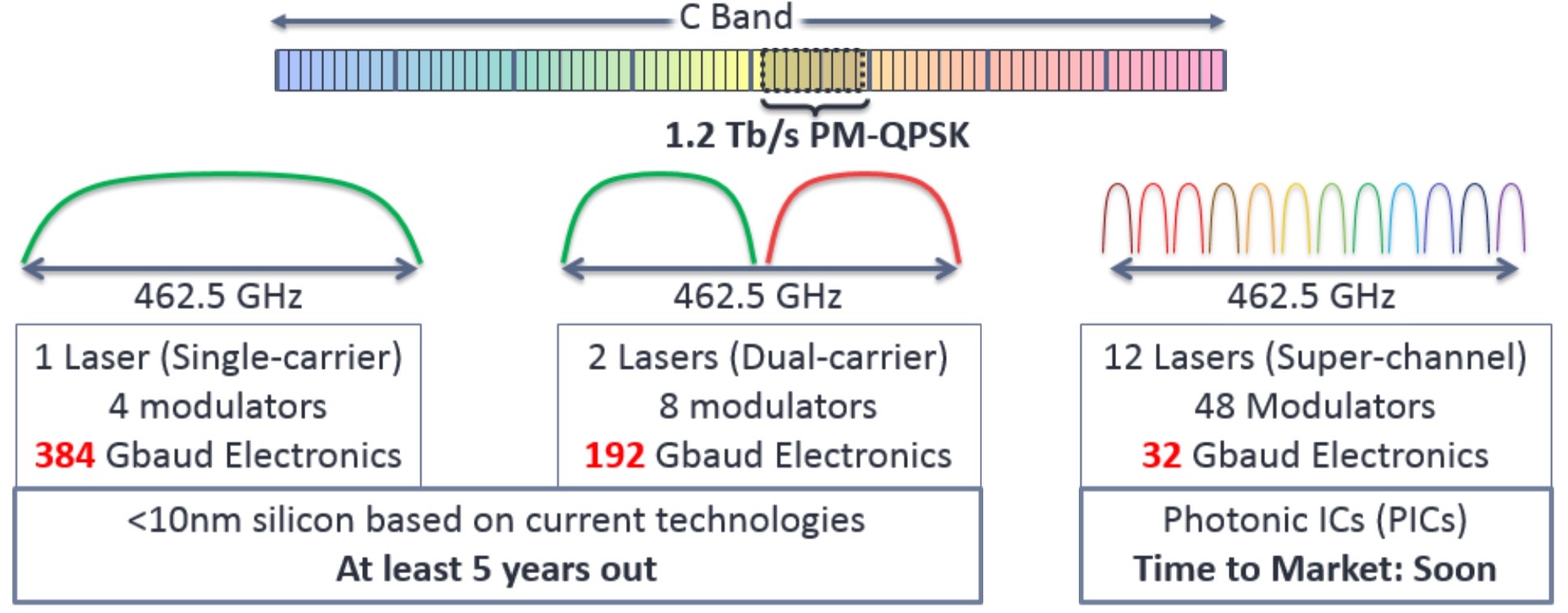
Spectral super-channels are used to create high bit-rate signals - 400 Gigabit and greater - by combining a number of sub-channels. Combining sub-channels is necessary since existing electronics can’t create such high bit rates using a single carrier.
Infinera points out that a 1.2 Terabit-per-second (Tbps) signal implemented using a single carrier would require 462.5 GHz of spectrum while the accompanying electronics to achieve the 384 Gigabaud (Gbaud) symbol rate would require a sub-10nm CMOS process, a technology at least five years away.
- Those that use non-overlapping sub-channels implemented using what is called Nyquist multiplexing.
- And those with overlapping sub-channels using orthogonal frequency division multiplexing (OFDM).

PMC advances OTN with 400 Gigabit processor
Optical modules for the line-side are moving beyond 100 Gigabits to 200 Gigabit and now 400 Gigabit transmission rates. Such designs are possible thanks to compact photonics designs and coherent DSP-ASICs implemented using advanced CMOS processes.
 An example switching application showing different configurations of the DIGi-G4 OTN processor on the line cards. Source: PMC
For engineers, the advent of higher-speed line-side interfaces sets new challenges when designing the line cards for optical networking equipment. In particular, the framer silicon that interfaces to the coherent DSP-ASIC, on the far side of the optics, must cope with a doubling and quadrupling of traffic.
Such line cards for metro network platforms is where PMC-Sierra is targeting its latest 400 Gigabit DIGI-G4 Optical Transport Network (OTN) processor.
The OTN standard, defined by the telecom standards body of the International Telecommunication Union (ITU-T), performs several roles in the network. It is a layer-one technology that packages packet and circuit-switched traffic. OTN wraps traffic in a variety of container sizes for transport, from 1 Gigabit (OTU1) to 100 Gigabit (OTU4). And now 100 Gigabit can be viewed as a sub-frame, multiples of which can be combined to create even larger frames, dubbed OTUCn, where n is a multiple of 100 Gig.
Using OTN, container traffic can be broken up, switched and recombined within new containers before being transmitted optically. OTN also provides forward error correction and network management features.
PMC’s DIGI-G4 OTN processor is aimed at next-generation packet-optical transport systems (P-OTS) adopting 400 Gig line cards, and for platforms for the burgeoning data centre interconnect market.
“The amounts of traffic internet content providers need between their data centres is astonishing; they are talking hundreds of terabits of traffic,” says Hamish Dobson, director of strategic marketing at PMC. Hyper-scale data centre operators, unlike telcos, do not require OTN switching but they are keen on OTN as the DWDM management layer, he says: “I’m not aware of any of the hyper-scale players who are deploying their own networks who are not using OTN as the un-channelised digital wrapper on their systems.”
The DIGI-G4 does more than simply quadruple OTN traffic throughput compared to PMC’s existing DIGI 120G OTN processor. The chip also adds encryption hardware to secure links while supporting the emerging Transport Software-Defined Networking (Transport SDN).
DIGI-G4
The DIGI-G4 increases by fourfold the traffic throughput while halving the power-per-port compared to PMC's DIGI 120G. System designers must control the total power consumption of the line card, given the greater interface density, and when metro equipment platforms’ power profile is already at 500W-per-slot, says Dobson. PMC has halved the power consumption-per-port by implementing the latest OTN processor in a 28 nm CMOS process and by using more power-efficient serialisers/ deserialisers (serdes).
Internet content providers with their use of distributed data centres is one reason for the device’s introduction of the Advanced Encryption Standard (AES-256). Another is the emergence of cloud services and the need to secure individual customer’s traffic.
“We have added a channelised hardware [encryption] engine,” says Dobson. “The encryption engine is capable of being applied to any OTN channel in the device.”
Other features of the Digi-G4 include input/ output (I/O) capable of 28 Gigabit-per-second (Gbps). This enables the DIGI-G4 to connect directly to CFP2 and CFP4 pluggable optics without the need for gearbox devices on the line card, reducing power and overall cost.
The OTN chip is a hybrid design capable of processing 400 Gigabit of packet traffic or 400 Gig of circuit (time-division multiplexed) traffic, or any combination of the two, with a granularity of one gigabit channels. “It can switch a full 400 Gig's worth of one Gigabit ODU0 channels,” says Dobson.
The Digi-G4 also support a pre-standard implementation of the OTUC2 and OTUC4 transport units that are two and four multiples of 100 Gigabit, respectively. The OTUCn standard is not expected to be ratified before 2017.

We will see the capabilities of these new packet-optical systems coming together with SDN to enable interesting things to be done in the metro
Hamish Dobson
Transport SDN
SDN will have a significant effect on the transport network, says Dobson. In particular Transport SDN where SDN is applied to the transport layers of the wide area network (WAN). As such, OTN plays an important role in multi-layer optimisation. Packet-optical transport systems, which support packet and optical within the same platform, are ideal for getting much more efficiency out of the optical spectrum, he says.
Using Transport SDN to co-ordinate packet, OTN and the optical layer, routing decisions can be made aware of available capacity in the optical domain. In turn, network protection decisions can also be based on optical capacity availability. “The DIGI-G4, being a hybrid processor to enable these multi-layer platforms, is an important element to bring this all together,” says Dobson.
OTN also aids the virtualisation of optical resources whereby individual enterprises can be given a simpler, subset view of the network. “We need more than just wavelength granularity in the network,” says Dobson. Since 100 Gigabit and, in future, 200 and 400 Gig lightwaves, are such large pipes, these are inevitably filled with multiple traffic flows. “Channelised OTN and OTN switching are how carriers are going to break down these massive amounts of optical capacity and partition them for various uses,” says Dobson.
A third element whereby OTN aids Transport SDN is the move to on-demand provisioning by adapting capacity at the OTN layer. Dobson cites the ITU-T G.7044/Y.1347 (G.HAO) standard, which the DIGI-G4 supports, whereby frame size can be adjusted using ODUflex without impacting existing network traffic.
“We will see the capabilities of these new packet-optical systems coming together with SDN to enable interesting things to be done in the metro,” says Dobson.
Samples of the DIGI-G4 are already with customers.
Further reading
White Paper: Benefits of OTN in Transport SDN, click here and then 'documentation'
Acacia unveils 400 Gigabit coherent transceiver
- The AC-400 5x7 inch MSA transceiver is a dual-carrier design
- Modulation formats supported include PM-QPSK, PM-8-QAM and PM-16-QAM
- Acacia’s DSP-ASIC is a 1.3 billion transistor dual-core chip
Acacia Communications has unveiled the industry's first flexible rate transceiver in a 5x7-inch MSA form factor that is capable of up to 400 Gigabit transmission rates. The company made the announcement at the OFC show held in Los Angeles.
Dubbed the AC-400, the transceiver supports 200, 300 and 400 Gigabit rates and includes two silicon photonics chips, each implementing single-carrier optical transmission, and a coherent DSP-ASIC. Acacia designs its own silicon photonics and DSP-ASIC ICs.
"The ASIC continues to drive performance while the optics continues to drive cost leadership," says Raj Shanmugaraj, Acacia's president and CEO.
The AC-400 uses several modulation formats that offer various capacity-reach options. The dual-carrier transceiver supports 200 Gig using polarisation multiplexing, quadrature phase-shift keying (PM-QPSK) and 400 Gig using 16-quadrature amplitude modulation (PM-16-QAM). The 16-QAM option is used primarily for data centre interconnect for distances up to a few hundred kilometers, says Benny Mikkelsen, co-founder and CTO of Acacia: "16-QAM provides the lowest cost-per-bit but goes shorter distances than QPSK."
Acacia has also implemented a third, intermediate format - PM-8-QAM - that improves reach compared to 16-QAM but encodes three bits per symbol (a total of 300 Gig) instead of 16-QAM's four bits (400 Gig). "8-QAM is a great compromise between 16-QAM and QPSK," says Mikkelsen. "It supports regional and even long-haul distances but with 50 percent higher capacity than QPSK." Acacia says one of its customer will use PM-8-QAM for a 10,000 km submarine cable application.
 Source: Gazettabyte
Other AC-400 transceiver features include OTN framing and forward error correction. The OTN framing can carry 100 Gigabit Ethernet and OTU4 signals as well as the newer OTUc1 format that allows client signals to be synchronised such that a 400 Gigabit flow from a router port can be carried, for example. The FEC options include a 15 percent overhead code for metro and a 25 percent overhead code for submarine applications.
The 28 nm CMOS DSP-ASIC features two cores to process the dual-carrier signals. According to Acacia, its customers claim the DSP-ASIC has a power consumption less than half that of its competitors. The ASIC used for Acacia’s AC-100 CFP pluggable transceiver announced a year ago consumes 12-15W and is the basis of its latest DSP design, suggesting an overall power consumption of 25 to 30+ Watts. Acacia has not provided power consumption figures and points out that since the device implements multiple modes, the power consumption varies.
The AC-400 uses two silicon photonics chips, one for each carrier. The design, Acacia's second generation photonic integrated circuit (PIC), has a reduced insertion loss such that it can now achieve submarine transmission reaches. "Its performance is on a par with lithium niobate [modulators]," says Mikkelsen.
It has been surprising to us, and probably even more surprising to our customers, how well silicon photonics is performing
The PIC’s basic optical building blocks - the modulators and the photo-detectors - have not been changed from the first-generation design. What has been improved is how light enters and exits the PIC, thereby reducing the coupling loss. The latest PIC has the same pin-out and fits in the same gold box as the first-generation design. "It has been surprising to us, and probably even more surprising to our customers, how well silicon photonics is performing," says Mikkelsen.
Acacia has not tried to integrate the two wavelength circuits on one PIC. "At this point we don't see a lot of cost savings doing that," says Mikkelsen. "Will we do that at some point in future? I don't know." Since there needs to be an ASIC associated with each channel, there is little benefit in having a highly integrated PIC followed by several discrete DSP-ASICs, one per channel.
The start-up now offers several optical module products. Its original 5x7 inch AC-100 MSA for long-haul applications is used by over 10 customers, while it has two 5x7 inch modules for submarine operating at 40 Gig and 100 Gig are used by two of the largest submarine network operators. Its more recent AC-100 CFP has been adopted by over 15 customers. These include most of the tier 1 carriers, says Acacia, and some content service providers. The AC-100 CFP has also been demonstrated working with Fujitsu Optical Components's CFP that uses NTT Electronics's DSP-ASIC. Acacia expects to ship 15,000 AC-100 coherent CFPs this year.
Each of the company's module products uses a custom DSP-ASIC such that Acacia has designed five coherent modems in as many years. "This is how we believe we out-compete the competition," says Shanmugaraj.
Meanwhile, Acacia’s coherent AC-400 MSA module is now sampling and will be generally available in the second quarter.
ClariPhy samples a 200 Gigabit coherent DSP-ASIC
The CL20010 is the first of ClariPhy's LightSpeed-II family of coherent digital signal processing ASICs (DSP-ASICs), manufactured using a 28nm CMOS process. "We believe it is the first 28nm standard product, and leaps ahead of the current generation [DSP-ASIC] devices," says Paul Voois, co-founder and chief strategy officer at ClariPhy.
 Paul Voois
ClariPhy has been shipping its 40 Gigabit coherent CL4010 LightSpeed chip since September 2011. Customers using the device include optical module makers Oclaro, NEC and JDSU. "We continue to go into new deployments but it is true that the 40 Gig market is not growing like the 100 Gig market," says Voois.
With the CL20010, Clariphy now joins NTT Electronics (NEL) as a merchant supplier of high-speed coherent silicon. Clariphy has said that the LightSpeed-II devices will address metro, long-haul and submarine.
No longer do the integrators need to buy a separate transmit multiplexer chip
Using an advanced 28nm CMOS process enables greater on-chip integration. The CL20010 includes the transmit and receive DSPs, soft-decision forward error correction, and mixed signal analogue-to-digital and digital-to-analogue converters. "No longer do the integrators need to buy a separate transmit multiplexer chip," says Voois.
The LightSpeed-II silicon also features an on-chip Optical Transport Network (OTN) framer/ mapper and a general-purpose processor. The general purpose processor enables the chip to be more network aware - for example, the state of a link - and support software-defined networking (SDN) in the WAN.
The LightSpeed-II ICs support three modulation schemes - polarisation-multiplexed, bipolar phase-shift keying (PM-BPSK), quadrature phase-shift keying (PM-QPSK) and 16-quadrature amplitude modulation (PM-16-QAM). Using PM-16-QAM, the CL20010 can support 200 Gigabit traffic. "I believe that is also a first for merchant silicon," says Voois.
Having an on-chip framer enables the transmission of two 100 Gigabit clients signals as a 200 Gigabit OTN signal. In turn, combining two CL20010 devices enables a 400 Gig flexible-grid super-channel to be transmitted. The on-chip transmit DSP enables the CL20010 to support flexible grid, with the dual carrier 400 Gigabit super-channel occupying 75GHz rather than 100GHz. The CL20010 can achieve a reach of 3,500km at 100 Gig, and over 600km at 200 and 400 Gig.
ClariPhy has not announced the power consumption of its chips but says that it is also targeting the metro pluggable market. Given that a CFP coherent module consumes up to 32W and that the optics alone consume 12W, a LightSpeed-II metro DSP-ASIC will likely consume 18-20W.
Merchant market
Many of the leading optical transport equipment makers, such as Alcatel-Lucent, Ciena, Cisco Systems, Huawei and Infinera, use their own coherent DSP-ASICs. More recently, Acacia Communications announced a CFP 100 Gig coherent pluggable module that uses its internally developed DSP-ASIC.
Some of the OEMs will continue to develop internal technology but even they can't cover all possible applications
ClariPhy says that despite the bulk of the 100 Gigabit coherent ports shipped use internally developed designs, there are signs that the market is moving towards adopting merchant silicon. "It doesn't happen all at once," says Voois. "Some of the OEMs will continue to develop internal technology but even they can't cover all possible applications."
He cites coherent silicon for metro networks as an example. Equipment makers are focussed on DSP-ASIC designs that satisfy the most demanding, ultra-long-haul network applications. But such high-performance, high-power chips are not suited for the more cost-conscious, low-power and compact metro requirements.
"Our committed customer base includes a nice spectrum of applications and integration types: OEMs and module vendors; metro, long haul and submarine," says Voois.
General availability of the CL20010 is expected later this year. The company will also be demonstrating the device at OFC 2014.
Ovum on Infinera's Intelligent Transport Network strategy
Infinera announced that TeliaSonera International Carrier (TSIC) is extending the use of its DTN-X to its European network, having already adopted the platform in the US. Infinera has also outlined the next evolution in its networking strategy, dubbed the Intelligent Transport Network.
 Dana Cooperson
Gazettabyte asked Dana Cooperson, vice president and practice leader, and Ron Kline, principal analyst, both in the network infrastructure group at market research firm, Ovum, about the announcement and Infinera's outlined strategy.
What has been announced
TSIC is adding Infinera's DTN-X to boost network capacity in Europe and accommodate its own growing IP traffic. TSIC already has deployed 100 Gig technology in its European network, using a Coriant product. The wholesale operator will sell 100 Gig services, activating capacity using the DTN-X's 'instant bandwidth' feature based on already-lit 100 Gig light paths that make up its 500 Gigabit super-channels.
Meanwhile, Infinera has detailed its Intelligent Transport Network strategy that extends its digital optical network that performs optical-electrical-optical (OEO) conversion using its 500 Gig photonic integrated circuits (PICs) coupled with OTN (Optical Transport Network) switching to include additional features. These include multi-layer switching – reconfigurable optical add/drop multiplexers (ROADMs) and MPLS (Multi-Protocol Label Switching) – and PICs with terabit capacity
Q&A with Dana Cooperson and Ron Kline
Q. What is significant about Infinera's Intelligent Transport Network strategy?
Dana C: Infinera is being more public about its longer-term strategy - to 2020 - which includes evolving from its digital optical network messaging to a network that includes multiple layers and types of switching, and more automation. Infinera is not announcing more functionality availability now.
Infinera makes much play about its 500 Gig super-channels. More recently it has detailed such platform features as instant bandwidth and Fast Shared Mesh Protection supported in hardware. Are these features giving operators something new and is Infinera gaining market share as a result?
Dana C: Instant Bandwidth provides a way for Infinera’s operator customers to have their cake and eat it. They can install 500 Gig super-channels ahead of demand, and not pay for each 100 Gig sub-channel until they have a need for that bandwidth. It is a simple process at that point to 'turn on' the next 100 Gig worth of bandwidth within the super-channel.
By installing all five 100 Gig channels at once, the operator can simplify operations - lower opex - and allow quicker time-to-revenue without having to take the capex hit until the bandwidth needs materialise. This is an improvement over the DTN platform, which gave customers the 10x10 Gig architecture to let them pre-position bandwidth before the need for it materialised and save on opex, but at the cost of higher up-front capex than was ideal.
Talking to TSIC confirm that this added flexibility the DTN-X provides has allowed them to win wholesale business from competitors while tying capex more directly to revenue.
Ron K: Although pay-as-you go capability is available, analysis of 100 Gig shipments to date indicate most customers are paying for all five up front.
Dana C: I have not directly talked with an Infinera customer that has confirmed the benefit of Fast Shared Mesh Protection, but the feature certainly seems to be of value to customers and prospects. Our research indicates the continued search for better, more efficient mesh protection. Hardware-enabled protection should provide better latency (higher speed).
Ron K: Resiliency and mesh protection are critical requirements if you want to participate in the market. Shared mesh assumes that you have idle protection capacity available in case there is a failure. That is expensive. However, with Infinera’s technology - the PIC and Instant Bandwidth - it is not as difficult.
Restoration is all about speed – how fast can you get the network back up. It is not always milliseconds, sometimes it is half a minute. But during catastrophic failure events such as an earthquake, where a user can loose entire nodes, 30 seconds may not be so bad. Infinera has implemented the switch in hardware, based on a pre-planned map, so it is quicker.
Dana C: As for what impact these capabilities are having on market share, Infinera has climbed to the No.3 player in 100 Gig DWDM in three quarters since the DTN-X has become available.
They’ve jumped back up to No.4 globally in backbone WDM/CPO-T (converged packet optical transport) after sinking to sixth when they were losing share because they were without a viable 40 Gig solution. They made the right call at that time to focus on 100 Gig systems based on the 500 Gig PIC rather than chase 40 Gig. They are both keeping and expanding with existing DTN customers, TSIC being one, and picking up new customers.
 Ron Kline
Ron K:They are definitely picking up share. However, I’m not sure if they can sustain it. The reason for the share jump is they are selling 100 Gig, five at a time. Remember, most customers elect to pay for all five. That means future sales will lag because customers have pre-positioned the bandwidth.
Looking at the customers is probably a better indicator: Infinera has some 27 customers, maybe 30 by now, which provide a good embedded base. Still, 27 customers is low compared to Ciena, Alcatel-Lucent, Huawei and even Cisco.
When Infinera first announced the DTN-X in 2011 it talked about how it would add MPLS support. Now outlining its Intelligent Transport Network strategy it has still to announce MPLS support. Do operators not need this network feature yet in such platforms and if not, why?
Dana C: The market is still sorting out exactly what is needed for sub-wavelength switching and where it is needed. Cisco’s and Juniper’s approaches are very different in the routing world —essentially, a lower-cost MPLS blade for the CRS versus a whole new box in the PTX; there is no right way there.
Within packet-aware optical products, the same is true: What is the right level of integration of OTN versus MPLS? It depends on where you are in the network, what that carrier’s service mix is, and how fast the mix is changing.
Many carriers are still struggling with their rigid organisational structures, and how best to manage products that are optical and packet in equal measure. So I don’t think Infinera is late, they are just reacting to their customers’ priorities and doing other things first.
Ron K: This is the $64,000 question: MPLS versus OTN. I’m not sure how it will eventually play out. I am asking service providers now.
OTN is a carrier protocol developed for carriers by carriers (the replacement for SONET/SDH). They will be the ones to use it because they have multi-service networks and need the transparency OTN provides. Google types and cable operators will not use OTN switching - they will lean towards the label-switched path (LSP) route. Even Tier-1 operators who have both types of networks will most likely maintain separation.
"The trick is to optimise around the requirements that net you the biggest total available market and which maximise your strengths and minimise your weaknesses. You can’t be all things to all carriers."
If Infinera has its digital optical network, why is it now also talking about ROADMs? And does having both benefit operators?
Dana C: Yes, having both benefits operators. From discussions with Infinera's customers, it is true that the digital nodes give them flexibility, but they do introduce added cost. For those nodes where customers have little need to add/ drop traffic, a ROADM would provide a more cost-efficient option to a node that performs OEO for all the traffic. So, with a ROADM option customers would have more control over node design.
Infinera talks about its next-gen PICs that will support a Terabit and more. After nearly a decade of making PICs, how does Ovum view the significance of the technology?
Dana C: While more vendors are doing photonic integration R&D, and some - Huawei comes to mind - have released some PIC-based products, no one has come close to Infinera in what it can do with photonic integration. Speaking with quite a few of Infinera’s customers, they are very happy with the technology, the system, and the support.
Each generation of PIC requires a significant R&D effort, but it does provide differentiation. Infinera has managed to stay focused and implement on time and on spec. I see them as the epitome of a “specialist” vendor. They are of similar size to Coriant and Tellabs, which have seen their fortunes wane, and ADVA Optical Networking. So I would say they are a very good example of what focus and differentiation can do.
Now, is the PIC the only way to approach system architecture? No. As noted before, some Infinera clients have told me that the lack of a ROADM has hurt them in competitive situations, as did the need to pay for all the pre-positioned bandwidth up front (true for the DTN, not the DTN-X).
From my days in product development, I know you have to optimise around a set of requirements, and the trick is to optimise around the requirements that net you the biggest total available market and which maximise your strengths and minimise your weaknesses. You can’t be all things to all carriers.
What is significant about the latest TeliaSonera network win and what does it mean for Coriant?
Dana C: Infinera is announcing an extension of its deployments at TSIC from North America to now include Europe as well. When you ask what this means to Coriant, their incumbent supplier in Europe, the answer is not clear cut. This gives Infinera an expanded hunting licence and it gives Coriant some cause for worry.
TSIC values both vendors and both will have their place in the European network. TSIC plans to use the vendors in different regions.
I am sure TSIC will try and play each off against the other to get the best price. It is looking for more flexibility and some healthy competition.
Apps over packet-optical: Ciena boosts 6500's packet handling
 Source: Ciena
Ciena has enhanced its packet-optical equipment portfolio by adding packet support to its flagship 6500 platform.
Cards and software from Ciena's established Carrier Ethernet packet platforms have been added to the 6500, a packet-optical platform that features reconfigurable optical add-drop multiplexing (ROADM), WaveLogic3 coherent transponders, Optical Transport Network (OTN) switching and SONET/SDH aggregation. The system vendor has also developed packet aggregation and switch fabric cards for the 6500.
"You can now use the 6500 for 100 percent packet switching, 100 percent OTN switching, or any mix in between," says Michael Adams, vice president of product and technical marketing at Ciena.
The development is part of a general trend to combine optical and packet to create scalable, manageable networks. It also addresses the operators' growing need for programmable networks to deliver cloud-based services and dynamic bandwidth.
Applications
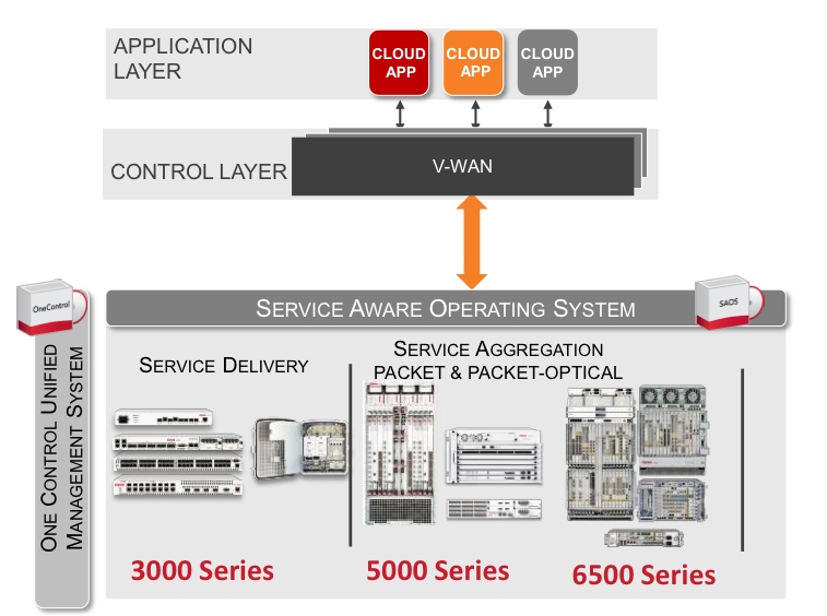
Ciena has a virtual wide-area network (VWAN) control layer that resides above the networking layer that abstracts the hardware and through which software applications can be executed (see chart).
"We have a scheduler 'app' through the control layer VWAN that allows bandwidth to change between sites, for example," says Adams. "Every night I want to do a backup between these times and I want this much bandwidth as I do it."
Another application is machine-to-machine communication that can be used to link data centres. "If you can virtualise within a data centre, why not virtualise across data centres?" says Adams.
As [servers'] virtual machines move between data centres, the performance of the network becomes key. Ciena has an application programming interface (API) that links to the server's hypervisor that allows machine-to-machine communication to be intercepted to benefit the bandwidth made available for the virtual machine traffic. "We are not doing it today but we have the software to link between two data centres," says Adams.
6500 enhancements
Until now it has been difficult to combine packet with packet optical, requiring different platforms, each with their own management system, says Adams. "It has been hard to take a base station that needs only packet, put the Carrier Ethernet traffic onto a ring [network] and then onto a 100 Gigabit wavelength," he says. "You either built pure packet or used a form of packet optical but it was hard to mix."
Ciena has added hardware and software to the 6500 from its existing packet platforms. The packet platforms are used to deliver Ethernet services and infrastructure and are a $40 million-a-quarter business for Ciena, with over 300,000 network elements deployed.
The service-aware operating system (SAOS), developed for the Ethernet packet platforms, has also been ported onto the 6500's new packet and fabric cards.
With the 6500 running the same software as its packet platforms, service management across the network becomes simpler. "Now, one system can deploy services, and look at performance visualisation between the layers," says Adams.
Ciena's latest hardware cards include blades with 1 and 10 Gigabit-per-second (Gbps) aggregation that operate independently of the 6500's switch fabric. "You don't touch the fabric, just run [them] over a WDM wavelength," says Adams. The stackable blades support 120Gbps to 300Gbps of packet traffic.
Meanwhile, the 6500 switch fabric cards add 600 Gigbit or 1.2 Terabit packet switching capacity that will be increased further in future.
"We have got these blades that can be stacked besides each other for resiliency or scale," says Adams. "And if you want to scale those up, there is a [switch] fabric solution."
Further reading:
100 Gigabit and packet optical loom large in the metro
P-OTS 2.0: 60-second interview with Heavy Reading's Sterling Perrin
P-OTS 2.0: 60s interview with Heavy Reading's Sterling Perrin
Q: Heavy Reading claims the metro packet optical transport system (P-OTS) market is entering a new phase. What are the characteristics of P-OTS 2.0 and what first-generation platform shortcomings does it address?
A: I would say four things characterise P-OTS 2.0 and separate 2.0 from the 1.0 implementations:
- The focus of packet-optical shifts from time-division multiplexing (TDM) functions to packet functions.
- Pure-packet implementations of P-OTS begin to ramp and, ultimately, dominate.
- Switched OTN (Optical Transport Network) enters the metro, removing the need for SONET/SDH fabrics in new elements.
- 100 Gigabit takes hold in the metro.
The last two points are new functions while the first two address shortcomings of the previous generation. P-OTS 1.0 suffered because its packet side was seen as sub-par relative to Ethernet "pure plays" and also because packet technology in general still had to mature and develop - such as standardising MPLS-TP (Multiprotocol Label Switching - Transport Profile).
Your survey's key findings: What struck Heavy Reading as noteworthy?
The biggest technology surprise was the tremendous interest in adding IP/MPLS functions to transport. There was a lot of debate about this 10 years ago. Then the industry settled on a de facto standard that transport includes layers 0-2 but no higher. Now, it appears that the transport definition must broaden to include up to layer 3.
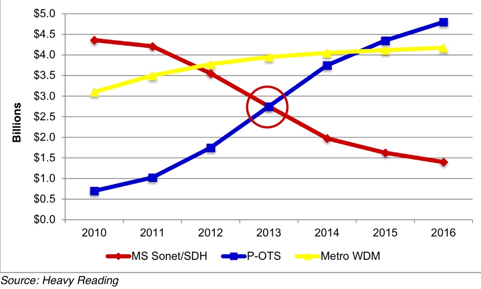
A second key finding is how quickly SONET/SDH has gone out of favour. Going forward, it is all about packet innovation. We saw this shift in equipment revenues in 2012 as SONET/SDH spend globally dropped more than 20 percent. That is not a one-time hit - it's the new trend for SONET/SDH.
Heavy Reading argues that transport has broadened in terms of the networking embraced - from layers 0 (WDM) and 1 (SONET/SDH and OTN) to now include IP/MPLS. Is the industry converging on one approach for multi-layer transport optimisation? For example, IP over dense WDM? Or OTN, Carrier Ethernet 2.0 and MPLS-TP? Or something else?
We did not uncover a single winning architecture and it's most likely that operators will do different things. Some operators will like OTN and put it everywhere. Others will have nothing to do with OTN. Some will integrate optics on routers to save transponder capital expenditure, but others will keep hardware separate but tightly link IP and optical layers via the control plane. I think it will be very mixed.
You talk about a spike in 100 Gigabit metro starting in 2014. What is the cause? And is it all coherent or is a healthy share going to 100 Gigabit direct detection?
Interest in 100 Gigabit in the metro exceeds interest in OTN in the metro - which is different from the core, where those two technologies are more tightly linked.
Cloud and data centre interconnect are the biggest drivers for interest in metro 100 Gig but there are other uses as well. We did not ask about coherent versus direct in this survey, but based on general industry discussions, I'd say the momentum is clearly around coherent at this stage - even in the metro. It does not seem that direct detect 100 Gig has a strong enough cost proposition to justify a world with two very different flavours of 100 Gig.
What surprised you from the survey's findings?
It was really the interest-level in IP functionality on transport systems that was the most surprising find.
It opens up the packet-optical transport market to new players that are strongest on IP and also poses a threat to suppliers that were good at lower layers but have no IP expertise - they'll have to do something about that.
Heavy Reading surveyed 114 operators globally. All those surveyed were operators; no system vendors were included. The regional split was North America - 22 percent, Europe - 33 percent, Asia Pacific - 25 percent, and the rest of the world - Latin America mainly - 20 percent.