
Using light to connect an AI processor’s cores
Lightelligence is using silicon photonics to connect 64 cores of its AI processor. But the company has bigger ambitions for its optical network-on-chip technology
Lightelligence has unveiled its optical network-on-chip designed to scale multiprocessor designs.
The start-up’s first product showcasing the technology is the Hummingbird, a system-in-package that combines Lightelligence’s 64-core artificial intelligence (AI) processor and a silicon photonics chip linking the processor’s cores.
A key issue impeding the scaling of computing resources is the ‘memory wall’ which refers to the growing gap between processor and memory speeds, causing processors to be idle as they wait for data to crunch.
“The memory wall is a genuine problem,” says Maurice Steinman, vice president of engineering at Lightelligence. “Even with the generational scaling of computing, the input-output (I/O) and access to off-chip communications are struggling to keep up.”
Lightelligence has developed Hummingbird to show how its optical networking approach could be used to scale multi-chip designs.
Origins
Lightelligence, an MIT spin-out, is a fabless chip company founded in 2017. The start-up has 200 engineers and has raised over $200 million in funding. Now, after five years, the company is beginning to generate revenues.
The company started by using nanophotonics to tackle such computations as matrix multiplications and linear algebra.
After two years, the focus broadened to include communications. There is no point in developing a low-latency analogue compute engine only to then encounter I/O and scaling issues, says Steinman.
Optical network-on-chip
The start-up is pursuing two communication tracks. The first is developing board-to-board or rack-to-rack communications based on optical transceivers and fibre. The second is communications at a smaller, system-in-package or chip-to-wafer scale, with Hummingbird and the optical network-on-chip being the first example.
“How do we address the challenges of purely electronic solutions today?” says Steinman. “How can we use photonics and an optical waveguide-based solution to get back some of the limitations there?”
The issue is that while chips can now have transistor counts in the tens of billions, a dimensions of the die are limited to some 800mm2, dictated by the reticule size. A multi-chip module or a chiplet approach is needed if additional computation is required.
“Ideally, you would want the performance to scale with the sum of silicon area; if I’ve got N chips, I want pure linear scaling,” says Steinman.
The issue with multiple chips is that they need interfaces which introduce communication and power consumption issues. And with an array of chips, a scheduler must oversee workload assignment to the processors as they become available.
“You’ve got all these interfaces, you’ve got queuing delay, you’ve got contention, you have multiple messages trying to contend for the same path,” says Steinman. “It is hard to see all that in multiple dimensions.”
Lightelligence wants to use optical networking to enable routing topologies linking compute resources that are impractical if attempted electronically.
“That’s the breakthrough we’re trying to bring to the world,” says Steinman. “What we are calling optical network-on-chip.”
The first implementation uses a network to link cores of a single-chip parallel processor, while the goal is to extend the networking beyond the chip scale, he says.
Lightelligence believes the technology will be attractive to silicon vendors facing similar scale-out issues. And by having a functioning device, the start-up has credibility when approaching potential customers.
“We want to work with them to design a purpose-built semi-custom solution because I’m sure every scale-out solution has different topology needs,” says Steinman.
Architecture
The Hummingbird device uses programmable cores that implement scalar, vector, and matrix operations, including 2D convolution. Such computations are accelerated using the optical network-on-chip with convolution used to implement a convolutional neural network for AI.
The chip includes a central instruction unit to implement a single-instruction, multiple-data (SIMD) architecture; each core performing the same operation on part of the data set.
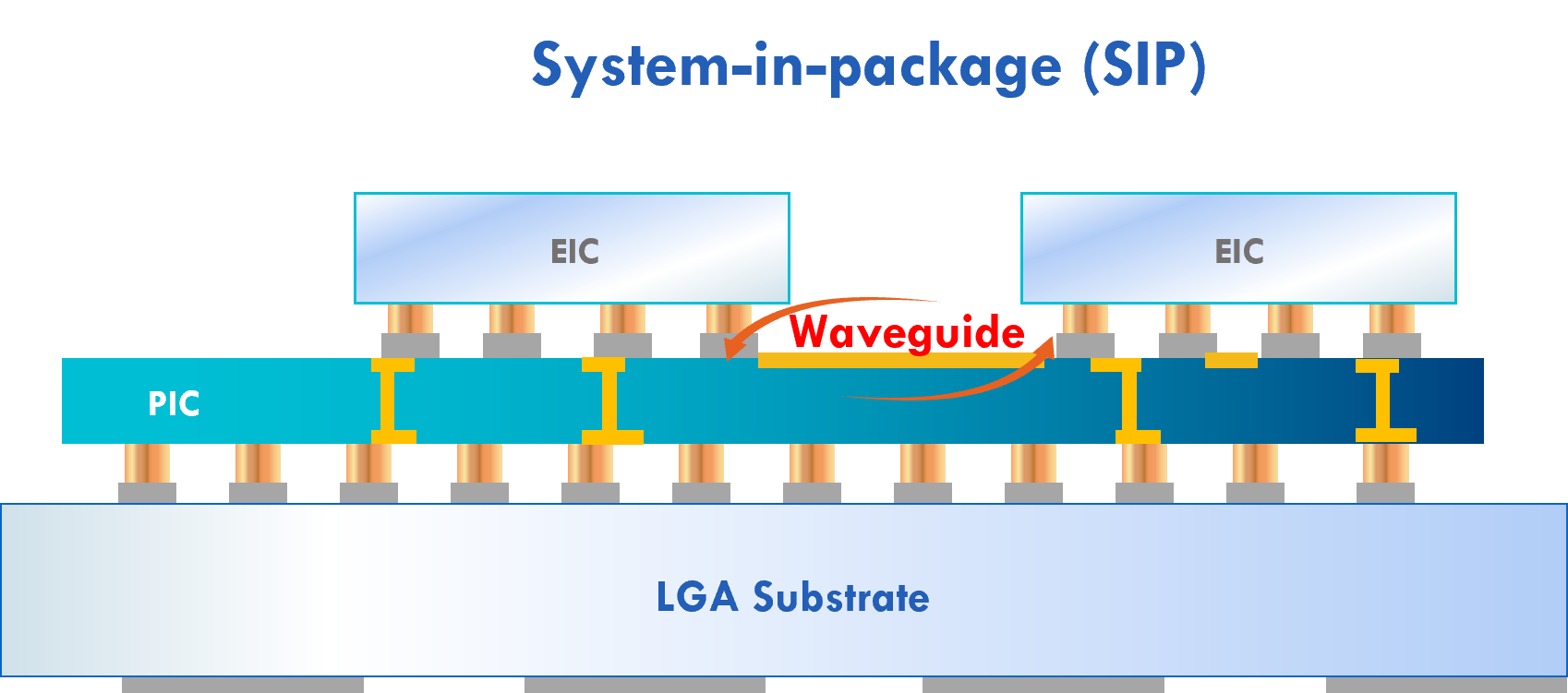
To aid the computation, each core has an optical broadcast transmitter. Every core can send and also receive data from every other core using the silicon photonics chip’s splitters and optical waveguides.
The ratio used by the optical-network-on-chip is 64 optical transmitters and 512 optical receivers rather than 64×64 optical receivers. This simplifies the optical design’s complexity, with electronics being used for the final stage to get data to particular cores in eight-core clusters.
“It is an all-to-all broadcast, an unusual topology,” says Steinman. “But in doing that, we have put a lot of transmitters and receivers on our companion photonic die that goes with the electronic [AI processor] die in Hummingbird.”
Lightelligence says the silicon photonics chip could implement other topologies, such as a 2D torus, for example.
Benefits
The motivation for the Lightelligence design is to achieve linear scaling, beyond what Hummingbird is showing for the single chip design. That said, the design already shows that many optical transmitters and receivers can be integrated into a dense space.
Lightelligence’s approach is also pragmatic. It has taken several years to develop Hummingbird and the start-up didn’t want to wait before developing a wafer-scale solution.
“There’s a little bit of constraining the problem to a single die, which is not the optimal proof point for it,” says Steinman. “But now we have a tangible working thing that gives us credibility for those higher-scale conversations.”
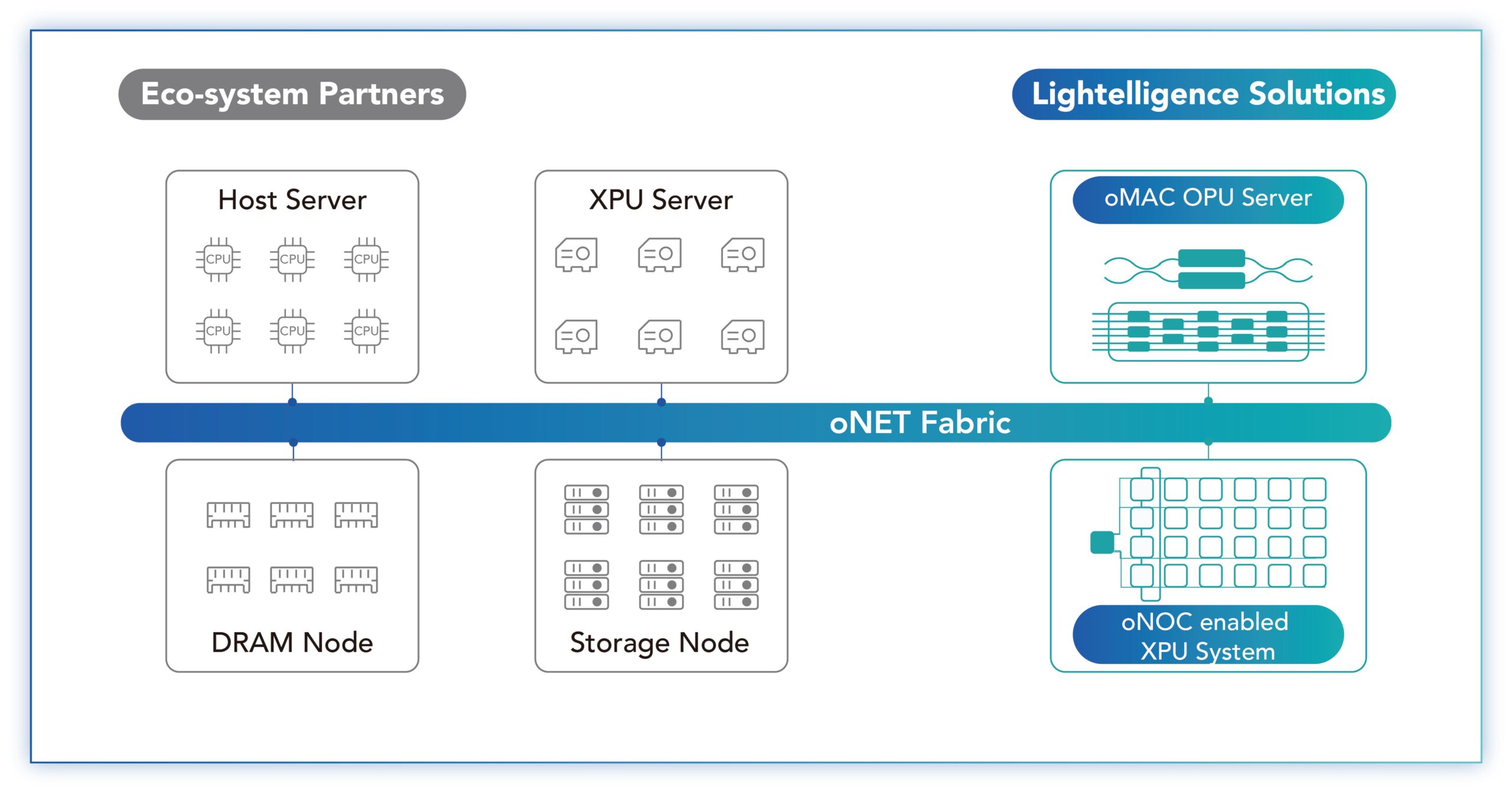
Steinman says the limit using the optical-network-on-chip technology is a wafer-sized design. Scaling beyond a wafer will require conventional optical interface technology (oNET, see diagram below) which Lightelligence is also developing.
Customers
The start-up has developed a PCI Express (PCIe) plug-in card that hosts the Hummingbird system-in-package. “It is a programmable machine; it does have an instruction set, compiler, and toolchain,” says Steinman.
Samples are with early adopter customers with AI inference tasks and Lightelligence is awaiting their feedback. “That next level of feedback is really important for our commercial objectives,” says Steinman.
Lightelligence also wants to partner with chip companies to start working on what Steinman calls ‘semi-custom’ engagements. “What are their problems that need to be solved, and how can we help?” he says.
Lightelligence will demonstrate the Hummingbird at the Hot Chips 2023 event in late August at Stanford University. Details of the device’s performance will also be revealed.

Neil McRae: What’s next for the telecom industry
In a talk at the FutureNet World conference, held in London on May 3-4, Neil McRae explains why he is upbeat about the telecoms industry’s prospects
Neil McRae is tasked with giving the final talk of the two-day FutureNet World conference.
“Yeah, I’m on the graveyard shift,” he quips.
McRae, the former chief network architect at BT, is now chief network strategist at Juniper Network.
The talk’s title is “What’s Next”, McRae’s take on the telecom industry and how it can grow.
McRae starts with how, as a 15-year-old, he had attended an Apple Macintosh computer event at a Novotel Hotel in Hammersmith, London, possibly even this one hosting this conference.
An Apple representative had asked for his feedback as a Macintosh programmer. McRae then listed all the shortfalls programming the PC. Later, he learnt that he had been talking to Steve Jobs.
Perhaps this explains his continual focus on customers and meeting their needs.
What customers care about, says McRae, is ‘new stuff’ that makes a difference in their lives. “Quite often in telecoms, we accidentally change the world without even thinking about it,” he says
McRae cites as an example using FaceTime to watch a newborn grandchild halfway across the world.
“We do it all the time; it is a phenomenal thing about our industry,” says McRae.
The Unvarnished Truth
McRae moves to showing several market and telco survey charts from IDC and Analysys Mason, what he calls ‘The unvarnished truth’.
The first slide shows how the European enterprise communication service market is set to grow at a compound annual growth rate (CAGR) of 3% between 2020 and 2025.
“Three per cent growth, who thinks that is a great business for telcos?” says McRae. “And enterprise is what we are all depending on for big growth and change because [the] consumer [market] is pretty much flat,” says McRae.
Another chart shows similar minimal growth: a forecast that Western Europe’s mobile retail service market will grow from $102 billion in 2016 to $109 billion by 2026. Yet mobile is where the telcos spend a ton of money, he says.
“So, who thinks we should continue doing what we are doing?” McRae asks the audience.
Another forecast showing global fixed and mobile service revenues is marginally better since it includes developing nations that still lack telecommunications services.
In the UK, 95 per cent of the population is on the internet, in Europe it is 84%, says McRae: “The UK is a tough place to be to grow business.”
Telco transformation
Another slide (see above), the results of a telco survey, shows a list of topics and their impact on telco transformation. McRae asks the audience to respond to those they think will ‘save’ the industry.
He goes through the list: cloud and cloudification, artificial intelligence (AI) and machine learning, 5G, and data analytics. The audience remains muted.
The next item is application programming interfaces (APIs). Again the audience is quiet. “You have been talking about APIs for two days!” says McRae.
“The right APIs,” shouts an audience member. “Ah, yes, the right APIs,” says McRae.
McRae continues down the list, virtualisation and software-defined infrastructure, OpenRAN elements – “not sure what the elements mean” – orchestration platforms, advanced process automation (OSS/BSS), micro-services, and blockchain.
McRae says he has spent the equivalent of a small nation’s budget over his career on OSS and BSS. “Nothing is automated, and I can’t get the data I need,” he says.
McRae gives his view. He believes the cloud will help telcos, but what most excites him is AI and machine learning, and data analytics.
“Learning the insights the data tells us and using them, putting a pound sign on them,” says McRae. “We have done some of that, but there is much more to do.”
He puts up a second survey showing the priorities of European operators: customer experience and increasing operational agility.
“Finally, after years, telcos realise that customers are important,” he says.
Opportunities
The survey also highlights the telcos’ belief that they can deliver solutions for industries and enterprise customers.
“This is a massive opportunity for telcos that allows us to grow revenues, create cool technology and hire amazing engineers,” says McRae.
The transformation needed in telecoms is about customers and taking risks with customers, he says.
One opportunity is digitalisation. McRae points outs that digitalisation is a process that never stops.
The three leading Chinese operators are keenly pursuing what they call industrial digitalisation or industrial internet. For China Telecom, industrial digitalisation now accounts for a quarter of its service revenues.
“Today, it is about cloud, cloud technologies, and smartphones, but tomorrow it could be about wearables or technology that is tracking what you are doing and making your life easier,” says McRae.
Digitalisation is an expertise that the telecom industry is not putting enough effort into, he says: “And as telcos, we have a massive right to play here.”
Another opportunity is AI and data, learning from the insights present in data to grow revenue.
“We have more data than most organisations, we haven’t used it very well, and we can build upon it,” says McRae, adding that AI needs the network to be valuable and improve our lives.
With data and AI, trust is vital. “If we are not trusted as an industry, we are dead,” says McRae. But because telcos are trusted entities, they can help other organisations improve trustworthiness.
Another opportunity is using the network for humans to interact in advanced ways. Since telecoms is a resource-heavy industry, such network-aided interaction would be immediately beneficial.
For this, what is needed is a cloud-native platform that integrates well with the network, and cloud platforms are generally poorly integrated with the network, he says.
He ends his talk by returning to customers and what they want: customers expect networks and services to be always present.
This explains the telcos’ continual marginal growth, he says: “The reason we have this is because there is a big chunk of customers’ lives where they can’t rely upon the network.”
Different thinking is needed if the network is to grow beyond the smartphone. Population coverage is not enough; what is needed is total coverage.
“Wherever I am, I want to use my device, to be connected, for the things that I don’t even know is doing stuff to be able to do them without worrying about connectivity,” he says.
And that is why 6G must be about 100 per cent connectivity,” says McRae: “Either we can do it, or someone else is going to.”
With that, FutureNet comes to ends, and McRae quickly departs to embark on the next chapter in his career. `
Neil McRae will be one of the speakers at the DSP Leaders World Forum, May 23-24, 2023.

Enfabrica’s chip tackles AI supercomputing challenges

- Enfabrica’s accelerated compute fabric chip is designed to scale computing clusters comprising CPUs and specialist accelerator chips.
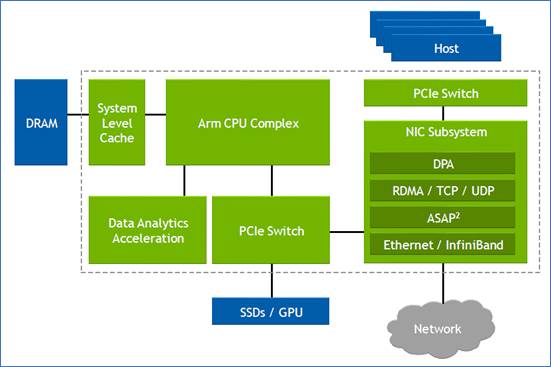
- The chip uses memory disaggregation and high-bandwidth networking for accelerator-based servers tackling artificial intelligence (AI) tasks.
For over a decade, cloud players have packed their data centres with x86-based CPU servers linked using tiers of Ethernet switches.
“The reason why Ethernet networking has been at the core of the infrastructure is that it is incredibly resilient,” says Rochan Sankar, CEO and co-founder of Enfabrica.
But the rise of AI and machine learning is causing the traditional architecture to change.
What is required is a mix of processors: CPUs and accelerators. Accelerators are specialist processors such as graphics processing units (GPUs), programmable logic (FPGAs), and custom ASICs developed by the hyperscalers.
It is the accelerator chips, not the CPUs, that do the bulk of the processing. Accelerators also require vast data, creating challenging input-output (I/O) and memory requirements.
At Optica’s Executive Forum event, held alongside the OFC show in March, Ryohei Urata, director and principal engineer at Google, mentioned how Google uses two computing pods – comprising 6,000 TPU accelerators – to run its large language models.
A key concern for Google is scaling such clusters while ensuring their reliability and availability. It is critical that the system is available when running a large language model, says Urata,
“As an engineer, when you’re putting stuff down, at least when you’re first start to put it together, you think, okay, this is going to work perfectly,” says Urata. “This is a perfect design, you don’t factor in failing gracefully, so that’s a key lesson.”
Google’s concern highlights that accelerator-based clusters lack the reliability of data centre server-Ethernet networks.
Accelerated compute fabric
Start-up Enfabrica has developed a chip, dubbed the accelerated compute fabric, to scale computing clusters.
“The focus of Enfabrica is on how networking and fabric technologies have to evolve in the age of AI-driven computing,” says Sankar.
AI models are growing between 8x to 275x annually, placing enormous demands on a data centre’s computing and memory resources.
“Two hundred and seventy-five times are of the order of what the large language models are increasing by, 8x is more other models including [machine] vision; recommender models are somewhere in between,” says Sankar.
Another AI hardware driver is growing end-user demand; ChatGPT gained 100 million users in the first months after its launch.
Meeting demand involves cascading more accelerators but the I/O bandwidth connected to the compute is lagging. Moreover, that gap is growing.
Sankar includes memory bandwidth as part of the I/O issue and segments I/O scaling into two: connecting CPUs, GPUs, accelerators and memory in the server, and the I/O scaling over the network.
A computing architecture for AI must accommodate greater CPUs and accelerators yet tackle the I/O bottleneck.
“To scale, it requires disaggregation; otherwise, it becomes unsustainable and expensive, or it can’t scale enough to meet processing demands,” says Sankar
“Memory disaggregation represents the last step in server disaggregation, following storage and networking,” says Bob Wheeler, principal analyst at Wheeler’s Network.
Memory expansion through disaggregation has become more urgent as GPUs access larger memories for AI training, particularly for large language modules like ChatGPT, says Wheeler.
Rethinking data connectivity
In the data centre, servers in a rack are linked using a top-of-rack switch. The top-of-rack switch also connects to the higher-capacity leaf-spine Ethernet switching layers to link servers across the data centre.
Enfabrica proposes that the higher capacity Ethernet switch leaf layer talks directly to its accelerated compute fabric chip, removing the top-of-rack switch.
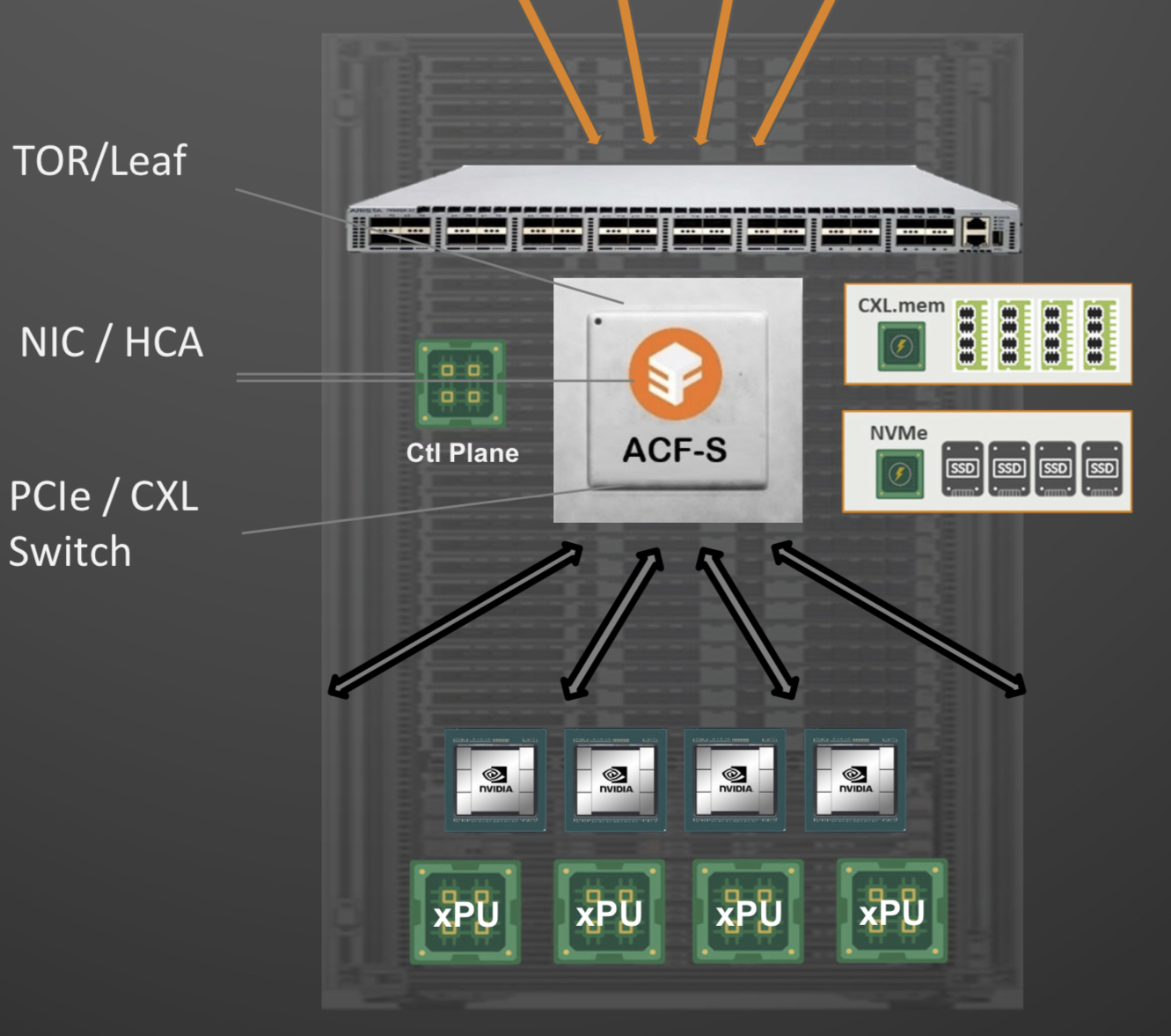
In turn, the accelerated compute fabric uses memory mapping to connect CPUs, accelerators, disaggregated memory pools using CXL, and disaggregated storage (see diagram above).
The memory can be a CPU’s DDR DRAM, a GPU’s high-bandwidth memory (HBM), a disaggregated compute express link (CXL) memory array, or storage.
“It [the accelerated compute fabric] connects to them over standard memory-mapped interfaces such as PCI Express (PCIe) or CXL,” says Sankar.
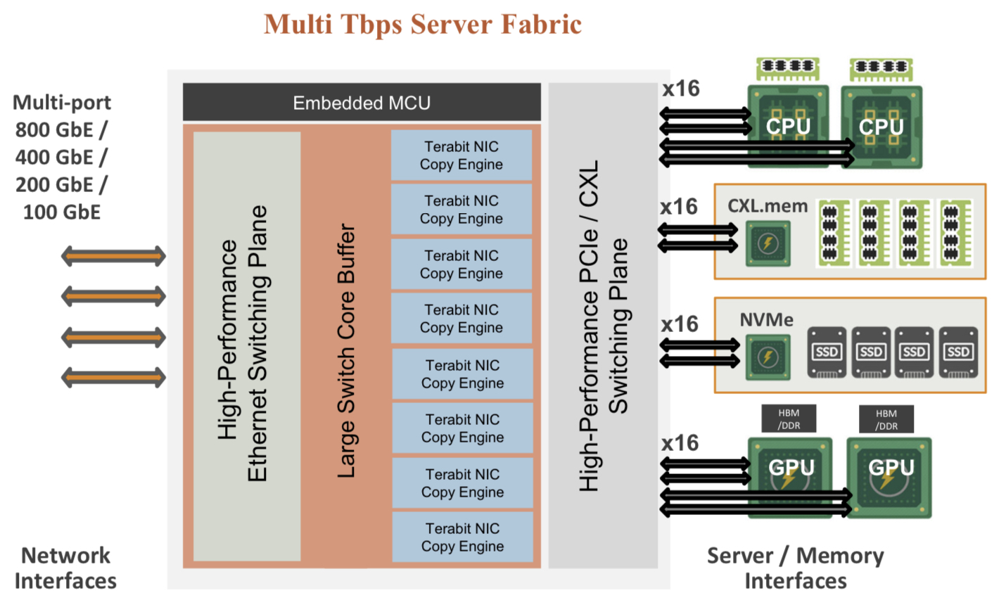
The chip uses ‘copy engines’ to move data to and from any processing element’s native memory. And by performing memory transfers in parallel, the chip is doing what until now has required PCIe switches, network interface cards (NICs), and top-of-rack switches.
The accelerated compute fabric also has 800-gigabit network interfaces so that, overall, the chip has terabits of bandwidth to move data across the network.
“CXL provides a standard way to decouple memories from CPUs, enabling DRAM disaggregation,” says Wheeler. “Enfabrica’s copy engines connect the GPUs to the pool of CXL memory. The network side, using RDMA (remote direct memory access), enables scaling beyond the limits of CXL.”
Sankar stresses that the accelerated compute fabric is much more than an integration exercise using an advanced 5nm CMOS process.
“If you were to integrate eight NICs, four PCIe switches and a top-of-rack switch, it would not fit into a single die,” says Sankar.
As for software, Enfabrica has designed its solution to fit in with how GPUs, CPUs and memory move data.
Significance
Sankar says the accelerated compute fabric IC will shorten job completion time because the scheduler is finer-grained and the chip can steer I/O to resources as required.
Computing clusters will also become larger using the IC’s high-density networking and CXL.
Wheeler says that CXL 3.x fabrics could provide the same capabilities as the accelerated compute fabric, but such advanced features won’t be available for years.
“History suggests some optional features included in the specifications will never gain adoption,” says Wheeler.
“The CXL/PCIe side of the [accelerated compute fabric] chip enables memory disaggregation without relying on CXL 3.x features that aren’t available, whereas the RNIC (RDMA NIC) side allows scaling to very large systems for workloads that can tolerate additional latency,” says Wheeler.
System benefits
Sankar cites two GPU platforms – one proprietary and one an open system – to highlight its chip benefits. The platforms are Nvidia’s DGX-H100 box and the open-design Grand Teton announced by Meta.
“The DGX has become a sort of fundamental commodity or a unit of AI computing,” says Shankar.
The DGX uses eight H100 GPUs, CPUs (typically two), I/O devices that link the GPUs using NVlink, and Infiniband for networking. The Meta platform has a similar specification but uses Ethernet.
Both systems have eight 400-gigabit interfaces. “That is 3.2 terabits coming out of the appliance, and inside the device, there is 3.2 terabit connected to a bunch of compute resources,” says Sankar.
The Meta platform includes layers of PCIe switches, and Open Compute Project (OCP 3.0) NICs running at 200 gigabits, going to 400 gigabits in the next generation.
The Grand Teton platform also uses eight NICs, four PCIe switches, and likely a top-of-rack switch to connect multiple systems.
Enfabrica’s vision is to enable a similarly composable [GPU] system. However, instead of eight NICs, four PCIe switches and the external top-of-rack switch, only three devices would be needed: two Enfabrica accelerated compute fabric chips and a control processor.
Enfabrica says the design would halve the power compared to the existing NICs, PCIe switches and the top-of-rack switch. “That represents 10 per cent of the rack’s power,” says Sankar.
And low-latency memory could be added to the space saved by using three chips instead of 12. Then, the eight GPUs would have tens of terabytes of memory to share whereas now each GPU has 80 gigabytes of HBM.
What next?
Enfabrica is unveiling the architecture first, and will detail its product later this year.
It is key to unveil the accelerated compute fabric concept now given how AI architectures are still nascent, says Sankar.
But to succeed, the start-up must win a sizeable data-centre customer such as a hyperscaler, says Wheeler: “That means there’s a very short list of customers, and winning one is paramount.”
The supplier must deliver high volumes from the start and guarantee supply continuity, and may also have to provide the source code to ensure that a customer can maintain the product under any circumstances.
“These are high hurdles, but Innovium proved it can be done and was rewarded with an exit at a valuation of greater than $1 billion,” says Wheeler.

Nvidia's plans for the data processor unit
When Nvidia’s CEO, Jensen Huang, discussed its latest 400-gigabit BlueField-3 data processing unit (DPU) at the company’s 2021 GTC event, he also detailed its successor.
Companies rarely discuss chip specifications two generations ahead; the BlueField-3 only begins sampling next quarter.
The BlueField-4 will advance Nvidia’s DPU family.
It will double again the traffic throughput to 800 gigabits-per-second (Gbps) and almost quadruple the BlueField-3’s integer processing performance.
But one metric cited stood out. The BlueField-4 will increase by nearly 1000x the number of terabit operators-per-second (TOPS) performed: 1,000 TOPS compared to the BlueField-3’s 1.5 TOPS.
Huang said artificial intelligence (AI) technologies will be added to the BlueField-4, implying that the massively parallel hardware used for Nvidia’s graphics processor units (GPUs) are to be grafted onto its next-but-one DPU.
Why add AI acceleration? And will it change the DPU, a relatively new processor class?
Data processor units
Nvidia defines the DPU as a programmable device for networking.
The chip combines general-purpose processing – multiple RISC cores used for control-plane tasks and programmed in a high-level language – with accelerator units tailored for packet-processing data-plane tasks.
“The accelerators perform functions for software-defined networking, software-defined storage and software-defined security,” says Kevin Deierling, senior vice president of networking at Nvidia.
The DPU can be added to a Smart Network Interface Card (SmartNIC) that complements the server’s CPU, taking over the data-intensive tasks that would otherwise burden the server’s most valuable resource.
Other customers use the DPU as a standalone device. “There is no CPU in their systems,” says Deierling.
Storage platforms is one such example, what Deierling describes as a narrowly-defined workload. “They don’t need a CPU and all its cores, what they need is the acceleration capabilities built into the DPU, and a relatively small amount of compute to perform the control-path operations,” says Deierling.
Since the DPU is the server’s networking gateway, it supports PCI Express (PCIe). The PCIe bus interfaces to the host CPU, to accelerators such as GPUs, and supports NVMe storage. NVMe is a non-volatile memory host controller interface specification.
BlueField 3
When announced in 2021, the 22-billion transistor BlueField-3 chip was scheduled to sample this quarter. “We need to get the silicon back and do some testing and validation before we are sampling,” says Deierling.
The device is a scaled-up version of the BlueField-2: it doubles the throughput to 400Gbps and includes more CPU cores: 16 Cortex-A78 64-bit ARM cores.
Nvidia deliberately chose not to use more powerful ARM cores. “The ARM is important, there is no doubt about it, and there are newer classes of ARM,” says Deierling. “We looked at the power and the performance benefits you’d get by moving to one of the newer classes and it doesn’t buy us what we need.”
The BlueField-3 has the equivalent processing performance of 300 X86 CPU cores, says Nvidia, but this is due mainly to the accelerator units, not the ARM cores.
The BlueField-3 input-output [I/O] includes Nvidia’s ConnectX-7 networking unit that supports 400 Gigabit Ethernet (GbE) which can be split over 1, 2 or 4 ports. The DPU also doubles the InfiniBand interface compared to the BlueField-2, either a single 400Gbps (NDR) port or two 200Gbps (HDR) ports. There are also 32 lanes of PCI Express 5.0, each lane supporting 32 giga-transfers-per-second (GT/s) in each direction.
The memory interface is two DDR5 channels, doubling both the memory performance and the channel count of the BlueField-2.
The data path accelerator (DPA) of the BlueField-3 comprises 16 cores, each supporting 16 instruction threads. Typically, when a packet arrives, it is decrypted and the headers are inspected after which the accelerators are used. The threads are used if the specific function needed is not accelerated. Then, a packet is assigned to a thread and processed.
“The DPA is a specialised part of our acceleration core that is highlighly programmable,” says Deierling.
Other programmable logic blocks include the accelerated switching and packet processing (ASAP2) engine that parses packets. It inspects packet fields looking for a match that tells it what to do, such as dropping the packet or rewriting its header.
In-line acceleration
The BlueField-3 implements the important task of security.
A packet can have many fields and encapsulations. For example, the fields can include a TCP header, quality of service, a destination IP and an IP header. These can be encapsulated into an overlay such as VXLAN and further encapsulated into a UDP packet before being wrapped in an outer IP datagram that is encrypted and sent over the network. Then, only the IPSec header is exposed; the remaining fields are encrypted.
Deierling says the BlueField-3 does the packet encryption and decryption in-line.
For example, the DPU uses the in-line IPsec decode to expose the headers of the various virtual network interfaces – the overlays – of a received packet. Picking the required overlay, the packet is sent to a set of service-function chainings that use all the accelerators available such as tackling distributed denial-of-service and implementing a firewall and load balancing.
“You can do storage, you can do an overlay, receive-side scaling [RSS], checksums,” says Deierling. “All the accelerations built into the DPU become available.”
Without in-line processing, the received packet goes through a NIC and into the memory of the host CPU. There, it is encrypted and hence opaque; the packet’s fields can’t benefit from the various acceleration techniques. “It is already in memory when it is decrypted,” says Deierling.
Often, with the DPU, the received packet is decrypted and passed to the host CPU where the full packet is visible. Then, once the host application has processed the data, the data and packet may be encrypted again before being sent on.
“In a ‘zero-trust’ environment, there may be a requirement to re-encrypt the data before sending it onto the next hop,” says Deierling. “In this case, we just reverse the pipeline.”
An example is confidential healthcare information where data needs to be encrypted before being sent and stored.
DPU evolution
There are many application set to benefit from DPU hardware. These cover the many segments Nvidia is addressing including AI, virtual worlds, robotics, self-driving cars, 5G and healthcare.
All need networking, storage and security. “Those are the three things we do but it is software-defined and hardware-accelerated,” says Deierling.
Nvidia has an ambitious target of launching a new DPU every 18 months. That suggests the BlueField-4 could sample as early as the end of 2023.
The 800-gigabit Bluefield-4 will have 64-billion transistors and nearly quadruple the integer processing performance of the BlueField-3: from 42 to 160 SPECint.
Nvidia says its DPUs, including the BlueField-4, are evolutionary in how they scale the ARM cores, accelerators and throughput. However, the AI acceleration hardware added to the BlueField-4 will change the nature of the DPU.
“What is truly salient is that [1,000] TOPS number,” says Deierling. “And that is an AI acceleration; that is leveraging capabilities Nvidia has on the GPU side.”
Self-driving cars, 5G and robotics
An AI-assisted DPU will support such tasks as video analytics, 5G and robotics.
For self-driving cars, the DPU will reside in the data centre, not in the car. But that too will change.“Frankly, the car is becoming a data centre,” notes Deierling.
Deep learning currently takes place in the data centre but as the automotive industry adopts Ethernet, a car’s sensors – lidar, radar and cameras – will send massive amounts of data which an IC must comprehend.
This is relevant not just for automotive but all applications where data from multiple sensors needs to be understood.
Deierling describes Nvidia as an AI-on-5G company.
“We have a ton of different things that we are doing and for that, you need a ton of parallel-processing capabilities,” he says. This is why the BlueField-4 is massively expanding its TOPS rating.
He describes how a robot on an automated factory floor will eventually understand its human colleagues.
“It is going to recognize you as a human being,“ says Deierling. “You are going to tell it: ‘Hey, stand back, I’m coming in to look at this thing’, and the robot will need to respond in real-time.”
Video analytics, voice processing, and natural language processing are all needed while the device will also be running a 5G interface. Here, the DPU will reside in a small mobile box: the robot.
“Our view of 5G is thus more comprehensive than just a fast pipe that you can use with a virtual RAN [radio access network] and Open RAN,” says Deierling. “We are looking at integrating this [BlueField-4] into higher-level platforms.”
Waiting for buses: PCI Express 6.0 to arrive on time

- PCI Express 6.0 (PCIe 6.0) continues the trend of doubling the speed of the point-to-point bus every 3 years.
- PCIe 6.0 uses PAM-4 signalling for the first time to achieve 64 giga-transfers per second (GT/s).
- Given the importance of the bus for interconnect standards such as the Compute Express Link (CXL) that supports disaggregation, the new bus can’t come fast enough for server vendors.
The PCI Express 6.0 specification is expected to be completed early next year.
So says Richard Solomon, vice-chair of the PCI Special Interest Group (PCI-SIG) which oversees the long-established PCI Express (PCIe) standard, and that has nearly 900 member companies.
The first announced products will then follow later next year while IP blocks supporting the 6.0 standard exist now.
When the work to develop the point-to-point communications standard was announced in 2019, developing lanes capable of 64 giga transfers-per-second (GT/s) in just two years was deemed ambitious, especially given 4-level pulse amplitude modulation (PAM-4) would be adopted for the first time.
But Solomon says the global pandemic may have benefitted development due to engineers working from home and spending more time on the standard. Demand from applications such as storage and artificial intelligence (AI)/ machine learning have also been driving factors.
Applications
The PCIe standard uses a dual simplex scheme – serial transmissions in both directions – referred to as a lane. The bus can be configured in several lane configurations: x1, x2, x4, x8, x12, x16 and x32, although x2, x12 and x32 are rarely used in practice.
PCIe 6.0’s transfer rate of 64GT/s is double that of the PCIe 5.0 standard that is already being adopted in products.
The PCIe bus is used for storage, processors, AI, the Internet of Things (IoT), mobile, and automotive especially with the advent of advanced driver assistance systems (ADAS). “Advanced driver assistance systems use a lot of AI; there is a huge amount of vision processing going on,” says Solomon.
For cloud applications, the bus is used for servers and storage. For servers, PCIe has been adopted by general-purpose processors and more specialist devices such as FPGAs, graphics processor units (GPUs) and AI hardware.
IBM’s latest 7nm POWER10 16-core processor, for example, is an 18-billion transistor device. The chip uses the PCIe 5.0 bus as part of its input-output.
In contrast, IoT applications typically adopt older generation PCIe interfaces. “It will be PCIe at 8 gigabit when the industry is on 16 and 32 gigabit,” says Solomon.
PCIe is being used for IoT because of it being a widely adopted interface and because PCIe devices interface like memory, using a load-store approach.
The CXL standard – an important technology for the data centre that interconnects processors, accelerator devices, memory, and switching – also makes use of PCIe, sitting on top of the PCIe physical layer.

PCIe roadmap
The PCIe 4.0 came out relatively late but then PCI-SIG quickly followed with PCIe 5.0 and now the 6.0 specification.
The PCIe 6.0 specification built into the schedule an allowance for some slippage while still being ready for when the industry would need the technology. But even with the adoption of PAM-4, the standard has kept to the original ambitious schedule.
PCIe 4.0 incorporated an important change by extending the number of outstanding commands and data. Before the 4.0 specification, PCIe allowed for up to 256 commands to be outstanding. With PCIe 4.0 that was tripled to 768.
To understand why this is needed, a host CPU system may support several add-in cards. When a card makes a read request, it may take the host a while to service the request, especially if the memory system is remote.
A way around that is for the add-in card to issue more commands to hide the latency.
“As the bus goes faster and faster, the transfer time goes down and the systems are frankly busier,” says Solomon. “If you are busy, I need to give you more commands so I can cover that latency.”
The PCIe technical terms are tags, a tag identifying each command, and credits which refers to how the bus takes care of flow control.
“You can think of tags as the sheer number of outstanding commands and credits as more as the amount of overall outstanding data,” says Solomon.
Both tags and credits had to be changed to support up to 768 outstanding commands. And this protocol change has been carried over into PCI 5.0.
In addition to the doubling in transfer rate to 32GT/s, PCI 5.0 requires an enhanced link budget of 36dB, up from 28dB with the PCIe 4.0. “As the frequency [of the signals] goes up, so does the loss,” says Solomon.
PCI 6.0
Moving from 32GT/s to 64GT/s and yet keep ensuring the same typical distances requires PAM-4.
More sophisticated circuitry at each end of the link is needed as well as a forward-error correction scheme which is a first for a PCI express standard implementation.
One advantage is that PAM-4 is already widely used for 56 and 112 gigabit-per-second high-speed interfaces. “That is why it was reasonable to set an aggressive timescale because we are leveraging a technology that is out there,” says Solomon. Here, PAM-4 will be operated at 64Gbps.
The tags and credits have again been expanded for PCI 6.0 to support 16,384 outstanding commands. “Hopefully, it will not be needed to be extended again,” says Solomon.
PCIe 6.0 also supports FLITs – a network packet scheme – that simplifies data transfers. FLITs are introduced with PCIe 6.0, but silicon designed for PCIe 6.0 could use FLITs at lower transfer speeds. Meanwhile, there are no signs of PCI Express needing to embrace optics as the interface speeds continue to advance.
“There is a ton of complexity and additional stuff we have to do to move to 6.0; optical would add to that,” says Solomon. “As long as people can do it on copper, they will keep doing it on copper.”
PCI-SIG is not yet talking about PCIe 7.0 but Solomon points out that every generation has doubled the transfer rate.

Turning to optical I/O to open up computing pinch points

Getting data in and out of chips used for modern computing has become a key challenge for designers.
A chip may talk to a neighbouring device in the same platform or to a chip across the data centre.
The sheer quantity of data and the reaches involved – tens or hundreds of meters – is why the industry is turning to optical for a chip’s input-output (I/O).
It is this technology transition that excites Ayar Labs.
The US start-up showcased its latest TeraPHY optical I/O chiplet operating at 1 terabit-per-second (Tbps) during the OFC virtual conference and exhibition held in June.
Evolutionary and revolutionary change
Ayar Labs says two developments are driving optical I/O.
One is the exponential growth in the capacity of Ethernet switch chips used in the data centre. The emergence of 25.6-terabit and soon 51.2-terabit Ethernet switches continue to drive technologies and standards.
This, says Hugo Saleh, vice president of business development and marketing, and recently appointed as the managing director of Ayar Labs’ new UK subsidiary, is an example of evolutionary change.
But artificial intelligence (AI) and high-performance computing have networking needs independent of the Ethernet specification.
“Ethernet is here to stay,” says Saleh. “But we think there is a new class of communications that is required to drive these advanced applications that need low latency and low power.”
Manufacturing processes
Ayar Labs’ TeraPHY chiplet is manufactured using GlobalFoundries’ 45nm RF Silicon on Insulator (45RFSOI) process. But Ayar Labs is also developing TeraPHY silicon using GlobalFoundries’ emerging 45nm CMOS-silicon photonics CLO process (45CLO).
The 45RFSOI process is being used because Ayar Labs is already supplying TeraPHY devices to customers. “They have been going out quite some time,” says Saleh.
But the start-up’s volume production of its chiplets will use GlobalFoundries’ 45CLO silicon photonics process. Version 1.0 of the process design kit (PDK) is expected in early 2022, leading to qualified TeraPHY parts based on the process.
One notable difference between the two processes is that 45RFSOI uses a vertical grating coupler to connect the fibre to the chiplet which requires active alignment. The 45CLO process uses a v-groove structure such that passive alignment can be used, simplifying and speeding up the fibre attachment.
“With high-volume manufacturing – millions and even tens of millions of parts – things like time-in-factory make a big difference,” says Saleh. Every second spent adds cost such that the faster the processes, the more cost-effective and scalable the manufacturing becomes.
Terabit TeraPHY
The TeraPHY chiplet demonstrated during OFC uses eight optical transceivers. Each transceiver comprises eight wavelength-division multiplexed (WDM) channels, each supporting 16 gigabit-per-second (Gbps) of data. The result is a total optical I/O bandwidth of 1.024Tbps operating in each direction (duplex link).
“The demonstration is at 16Gbps and we are going to be driving up to 25Gbps and 32Gbps next,” says Saleh.
The chiplet’s electrical I/O is slower and wider: 16 interfaces, each with 80, 2Gbps channels implementing Intel’s Advanced Interface Bus (AIB) technology.
Last December, Ayar Labs showcased advanced parts using the CLO process. The design was a direct-drive part – a prototype of a future-generation product, not the one demonstrated for OFC.
“The direct-drive part has a serial analogue interface that could come from the host ASIC directly into the ring resonators and modulate them whereas the part we have today is the productised version of an AIB interface with all the macros and all the bandwidth enabled,” says Saleh.
Ayar Labs also demonstrated its 8-laser light source, dubbed SuperNova, that drives the chiplet’s optics.
The eight distributed feedback (DFB) lasers are mixed using a planar lightwave circuit to produce eight channels, each comprising eight frequencies of light.
Saleh compares the SuperNova to a centralised power supply in a server that power pools of CPUs and memory. “The SuperNova mimics that,” he says. “One SuperNova or a 1 rack-unit box of 16 SuperNovas distributing continuous-wave light just like distributed voltage [in a server].”
The current 64-channel SuperNova powers a single TeraPHY but future versions will be able to supply light to two or more.
Ayar Labs is using Macom as its volume supplier of DFB lasers.
Significance
Ayar Labs believes the 1-terabit chip-to-chip WDM link is an industry first.
The demo also highlights how the company is getting closer to a design that can be run in the field. The silicon was made less than a month before the demonstration and was assembled quickly. “It was not behind glass and was operating at room temperature,” says Saleh. “It’s not a lab setting but a production setting.”
The same applies to the SuperNova. The light source is compliant with the Continuous-Wave Wavelength Division Multiplexing (CW-WDM) Multi-Source Agreement (MSA) Group that released its first specification revision to coincide with OFC. The CW-WDM MSA Group has developed a specification for 8, 16, and 32-wavelength optical sources.
The CW-WDM MSA promoter and observer members include all the key laser makers as well as the leading ASIC vendors. “We hope to establish an ecosystem on the laser side but also on the optics,” says Saleh.
“Fundamentally, there is a change at the physical (PHY) level that is required to open up these bottlenecks,” says Saleh. “The CW-WDM MSA is key to doing that; without the MSA you will not get that standardisation.”
Saleh also points to the TeraPHY’s optical I/O’s low power consumption which for each link equates to 5pJ/bit. This is about a tenth of the power consumed by electrical I/O especially when retimers are used. Equally, the reach is up to 2km not tens of centimetres associated with electrical links.
Chiplet demand
At OFC, Arista Networks outlined how pluggable optics will be able to address 102.4 terabit Ethernet switches while Microsoft said it expects to deploy co-packaged optics by the second half of 2024.
Nvidia also discussed how it clusters its graphics processing units (GPUs) that are used for AI applications. However, when a GPU from one cluster needs to talk to a GPU in another cluster, a performance hit occurs.
Nvidia is looking for the optical industry to develop interfaces that will enable its GPU systems to scale while appearing as one tightly coupled cluster. This will require low latency links. Instead of microseconds and milliseconds depending on the number of hops, optical I/O reduces the latency to tens of nanoseconds.
“We spec our chiplet as sub-5ns plus the time of flight which is about 5ns per meter,” says Saleh. Accordingly, the transit time between two GPUs 1m apart is 15ns.
Ayar Labs says that after many conversations with switch vendors and cloud players, the consensus is that Ethernet switches will have to adopt co-packaged optics. There will be different introductory points for the technology but the industry direction is clear.
“You are going to see co-packaged optics for Ethernet by 2024 but you should see the first AI fabric system with co-packaged I/O in 2022,” says Saleh.
Intel published a paper at OFC involving its Stratix 10 FPGA using five Ayar Labs’ chiplets, each one operating at 1.6 terabits (each optical channel operating at 25Gbps, not 16Gbps). The resulting FPGA has an optical I/O capacity of 8Tbps, the design part of the US DARPA PIPES (Photonics in the Package for Extreme Scalability) project.
“A key point of the paper is that Intel is yielding functional units,” says Saleh. The paper also highlighted the packaging and assembly achievements and the custom cooling used.
Intel Capital is a strategic investor in Ayar Labs, as is GlobalFoundries, Lockheed Martin Ventures, and Applied Materials.

Ayar Labs’ TeraPhy chiplet nears volume production
Moving data between processing nodes - whether servers in a data centre or specialised computing nodes used for supercomputing and artificial intelligence (AI) - is becoming a performance bottleneck.
Workloads continue to grow yet networking isn’t keeping pace with processing hardware, resulting in the inefficient use of costly hardware.
Networking also accounts for an increasing proportion of the overall power consumed by such computing systems.
These trends explain the increasing interest in placing optics alongside chips and co-packaging the two to boost input-output (I/O) capacity and reach.
At the ECOC 2020 exhibition and conference held virtually, start-up Ayar Labs showcased its first working TeraPHY, an optical I/O chiplet, manufactured using GlobalFoundries’ 45nm silicon-photonics process.
GlobalFoundries is a strategic investor in Ayar Labs and has been supplying Ayar Labs with TeraPHY chips made using its existing 45nm silicon-on-insulator process for radio frequency (RF) designs.
The foundry’s new 300mm wafer 45nm silicon-photonics process follows joint work with Ayar Labs, including the development of the process design kit (PDK) and standard cells.
“This is a process that mixes optics and electronics,” says Hugo Saleh, vice president of marketing and business development at Ayar Labs (pictured). “We build a monolithic die that has all the logic to control the optics, as well as the optics,” he says.
The latest TeraPHY design is an important milestone for Ayar Labs as it looks to become a volume supplier. “None of the semiconductor manufacturers would consider integrating a solution into their package if it wasn’t produced on a qualified high-volume manufacturing process,” says Saleh.
Applications
The TeraPHY chiplet can be co-packaged with such devices as Ethernet switch chips, general-purpose processors (CPUs), graphics processing units (GPUs), AI processors, and field-programmable gate arrays (FPGAs).
Ayar Labs says it is engaged in several efforts to add optics to Ethernet switch chips, the application most associated with co-packaged optics, but its focus is AI, high-performance computing and aerospace applications.
Last year, Intel and Ayar Labs detailed a Stratix 10 FPGA co-packaged with two TeraPHYs for a phased-array radar design as part of a DARPA PIPES and the Electronics Resurgence Initiative backed by the US government.
Adding optical I/O chiplets to FPGAs suits several aerospace applications including avionics, satellite and electronic warfare.
TeraPHY chiplet
The ECOC-showcased TeraPHY uses eight transmitter-receiver pairs, each pair supporting eight channels operating at either 16, 25 or 32 gigabit-per-second (Gbps), to achieve an optical I/O of up to 2.048 terabits.
The chiplet can use either a serial electrical interface or Intel’s Advanced Interface Bus (AIB), a wide-bus design that uses slower 2Gbps channels. The latest TeraPHY uses a 32Gbps non-return-to-zero (NRZ) serial interface and Saleh says the company is working on a 56Gbps version.
The company has also demonstrated 4-level pulse-amplitude modulation (PAM-4) technology but many applications require the lowest latency links possible.
“PAM-4 gives you a higher data rate but it comes with the tax of forward-error correction,” says Saleh. With PAM-4 and forward-error correction, the latency is hundreds of nanoseconds (ns), whereas the latency is 5ns using a NRZ link.
Ayar Labs’s next parallel I/O AIB-based TeraPHY design will use Intel’s AIB 1.0 specification and will use 16 cells, each having 80, 2Gbps channels, to achieve a 2.5Tbps electrical interface.
In contrast, the TeraPHY used with the Stratix 10 FPGA has 24 AIB cells, each having 20, 2Gbps channels for an overall electrical bandwidth of 960 gigabits, while its optical I/O is 2.56Tbps since 10 transmit-receive pairs are used.
The optical bandwidth is deliberately higher than the electrical bandwidth. First, not all the transmit-receive macros on the die need to be used. Second, the chiplet has a crossbar switch that allows one-to-many connections such that an electrical channel can be sent out on more than one optical interface and vice versa.
Architectures
Saleh points to several recent announcements that highlight the changes taking place in the industry that are driving new architectural developments.
He cites AMD acquiring programmable logic player, Xilinx; how Apple instances are now being hosted in Amazon Web Services’ (AWS) cloud to aid developers and Apple's processors, and how AWS and Microsoft are developing their own processors.
“Processors can now be built by companies using TSMC’s leading process technology using the ARM and RISC-V processor ecosystems,” he says. “AWS and Microsoft can target their codebase to whatever processor they want, including one developed by themselves.”
Saleh notes that Ethernet remains a key networking technology in the data centre and will continue to evolve but certain developments do need something else.
Applications such as AI and high-performance computing would benefit from a disaggregated design whereby CPUs, GPUs, AI devices and memory are separated and pooled. An application can then select the hardware it needs for the relevant pools to create the exact architecture it needs.
“Some of these new applications and processors that are popping up, there is a lot of benefit in a one-to-one and one-to-many connections,” he says. “The Achilles heel has always been how you disaggregate the memory because of latency and power concerns. Co-packaged optics with the host ASIC is the only way to do that.”
It will also be the only way such disaggregated designs will work given that far greater connectivity - estimated to be up to 100x that of existing systems - will be needed.
Expansion
Ayar Labs announced in November that it had raised $35 million in the second round of funding which, it says, was oversubscribed. This adds to its previous funding of $25 million.
The latest round includes four new investors and will help the start-up expand and address new markets.
One investor is a UK firm, Downing, that will connect Ayar Labs to European R&D and product opportunities. Saleh mentions the European Processor Initiative (EPI) that is designing a family of low-power European processors for extreme-scale computing. “Working with Downing, we are getting introduced into some of these initiatives including EPI and having conversations with the principals,” he says.
In turn, SGInnovate, a venture capitalist funded by the Singapore government, will help expand Ayar Labs’ activities in Asia. The two other investors are Castor Ventures and Applied Ventures, the investment arm of Applied Materials, the supplier of chip fabrication plant equipment.
“Applied Materials want to partner with us to develop the methodologies and tools to bring the technology to market,” says Saleh.
Meanwhile, Ayar Labs continues to grow, with a staff count approaching 100.

Xilinx’s Versal Premium ready for the 800-gigabit era
When Xilinx was created in 1984, the founders banked on programmable logic becoming ever more attractive due to Moore’s law.
Making logic programmable requires extra transistors so Xilinx needed them to become cheaper and more plentiful, something Moore’s law has delivered, like clockwork, over decades.
Since then, Xilinx’s field-programmable gate array (FPGA) devices have advanced considerably.
Indeed, Xilinx’s latest programmable logic family, the Versal Premium, is no longer referred to as an FPGA but as an adaptive compute accelerator platform (ACAP).
The Versal Premium series of chips, to be implemented using TSMC’s 7nm CMOS process, was unveiled for the OFC 2020 show. The Premium series will have seven chips with the largest, the VP1802, having 50 billion transistors.
First devices will ship in the second half of 2021.
ACAP series
Xilinx unveiled its adaptive compute acceleration platform in 2018.

Kirk Saban
“It is a complete rearchitecting of our device technology,” says Kirk Saban, vice president product and platform marketing at Xilinx. “It is heterogenous by nature and has multiple types of processing engines.”
“Versal Premium is evolutionary compared with previous FPGAs that have hardened blocks for certain functions,” says Bob Wheeler, principal analyst at The Linley Group. “It is another step along a continuum, not really new.”
Six ACAP families are planned for Versal: three tailored for artificial intelligence (AI) - the AI RF, AI Core and AI Edge - and the others being the Prime, Premium and HBM (high bandwidth memory).
Only Versal AI series will have AI engines: very-long-instructing-word (VLIW) processor cores that can also be used for computational-intensive tasks such as digital signal processing.
Premium is the third Versal family to be unveiled, joining the AI Core and Prime series.
Versal Prime is Xilinx’s broadest series in the portfolio, featuring a range of device sizes and capabilities. The Prime series is suited to such applications as storage acceleration in the data centre; wired networking such as 5G back-, mid- and front-haul, and passive optical networking; and industrial applications such as machine vision.
Networking needs
Versal Premium has been developed with core networking and data centre acceleration applications in mind.
“The top-end SKU handles high-end networking applications such as optical transport and data centre interconnect as well as the most demanding signal-processing applications such as radar systems,” says Wheeler.
Xilinx defines core networking as the infrastructure beyond the radio access network. “All the wireline infrastructure is what we consider to be the core of the network,” says Saban. “Access, metro, and core networks, all together.”
When Xilinx’s designers sat down to consider the networking needs for the coming six years, they anticipated a huge capacity hike in the core network. Device numbers are set to grow tenfold with each device generating ten times more traffic.
“The bandwidth going through the wired network globally needs to grow at 50 per cent on a compound annual basis to keep pace with the number of devices being connected and the data coming through them,” says Saban.
Versal Premium will deliver three times the bandwidth and nearly twice the logic capacity of the 16nm Virtex UltraScale+ VU13P FPGA, the largest device used currently for networking and data centre applications.
“Shifts are happening that the Virtex FPGAs are not going to be able to handle,” says Saban. “The move to 400 gigabit and then 800 gigabit on the mid-term horizon, the Virtex products can’t handle that kind of throughput.”
Versal Premium architecture. Source: Xilinx
Premium architecture
The Premium devices feature ARM-based scalar processors such as the dual-core Cortex-A72 application processor and the dual-core Cortex-R5F real-time processor.
The application processor is used for general-purpose processing and control. The real-time processor is used for applications that require deterministic processing. Such a processor is key for safety-certified applications.
Also included is a platform management controller that oversees the device. A user can configure many of the ACAP settings using a standard tool flow but the controller’s operation is effectively transparent to the user, says Saban.
The Premium features several types of on-chip memory that Saban likens to levels of cache memory used by high-performance processors. ”We have look-up-table RAM, Block RAM and Ultra RAM and we can offload to [external] DDR4 [RAM],” he says. “The memory hierarchy can be configured to match the algorithm you are building.”
The various on-chip functional blocks are linked via a programmable network-on-a-chip. Having the network-on-a-chip frees up programmable logic resources that would otherwise be required to connect the design’s functional blocks.
“Equipment manufacturers need to deliver on this core network growth but they also need to do it securely,” says Saban. “With everything shifting to the cloud, there are huge concerns about data privacy; in many instances, security is just as important as performance for the operators.”
To this aim, the Premium’s on-chip peripherals include 400-gigabit crypto-engines that support the AES-GCM-256 and -128, MACsec, and IPSec encryption standards.
“The crypto blocks are unique and save a lot of look-up tables and power compared with implementing these in programmable logic,” says Linley’s Wheeler.
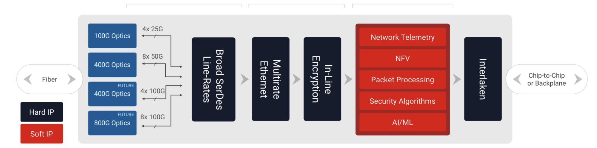
Other on-chip features include up to 5 terabits of Ethernet throughput supporting rates from 10 to 400 Gigabit Ethernet. The devices have multiple 600-gigabit Ethernet MAC cores and support such protocols as FlexE, Flex-O, Ethernet CPRI (eCPRI), Fibre Channel over Ethernet (FCoE), and OTN.
The Premium family delivers up to 1.8 terabits of Interlaken, from 10-gigabit to 600-gigabit interfaces. Interlaken enables chip-to-chip and chip-to-backplane communications.
There are also 112-gigabit 4-level pulse-amplitude modulation (PAM-4) serialisers/ deserialisers (serdes). The VP1802 will have 28, 32-gigabit serdes and either 140, 58-gigabit or 70, 112-gigabit serdes. The electrical transceivers can drive 10m of copper cable, says Saban.
PCI Express Generation 5.0, enabling direct memory access and cache-coherent interconnect, is also supported on-chip. “We can connect to server CPUs and be an extension of their memory map,” says Saban.
Xilinx claims 22 UltraScale+ FPGAs would be needed to implement all the logic and peripherals of the Versal Premium VP1802.
System design
Wireline vendors want to double the performance with each generation of equipment while keeping platform size and power consumption constant.
Xilinx has a diagram (shown) of a generic telecom line-card design using the Versal Premium. “Vendors have different variants but at a high-level, they all look like this,” says Saban.
Generic telecom line card using the Versal Premium. Source: Xilinx
Line-card data arrives via optical modules. At present 100-gigabit is mainstream with 400-gigabit coming soon, and eventually 800-gigabit interfaces. The data is fed to the Premium’s hardened logic blocks: the Ethernet and encryption blocks.
The adaptive logic (in red) is what companies use to implement their unique designs such as executing virtualised network functions (NFV) or for packet processing.
“We are seeing the need to infuse artificial intelligence and machine learning into these applications in some capacity,” says Saban. Premium devices have no AI VLIW cores but have sufficient resources for some level of artificial intelligence/ machine learning capability.
Interlaken then sends the data to a host chip or across the backplane to another line card.
Software tools
Xilinx stresses the company is no longer a chip provider but a platform provider. This is reflected in the software tools it provides to accompany its silicon.
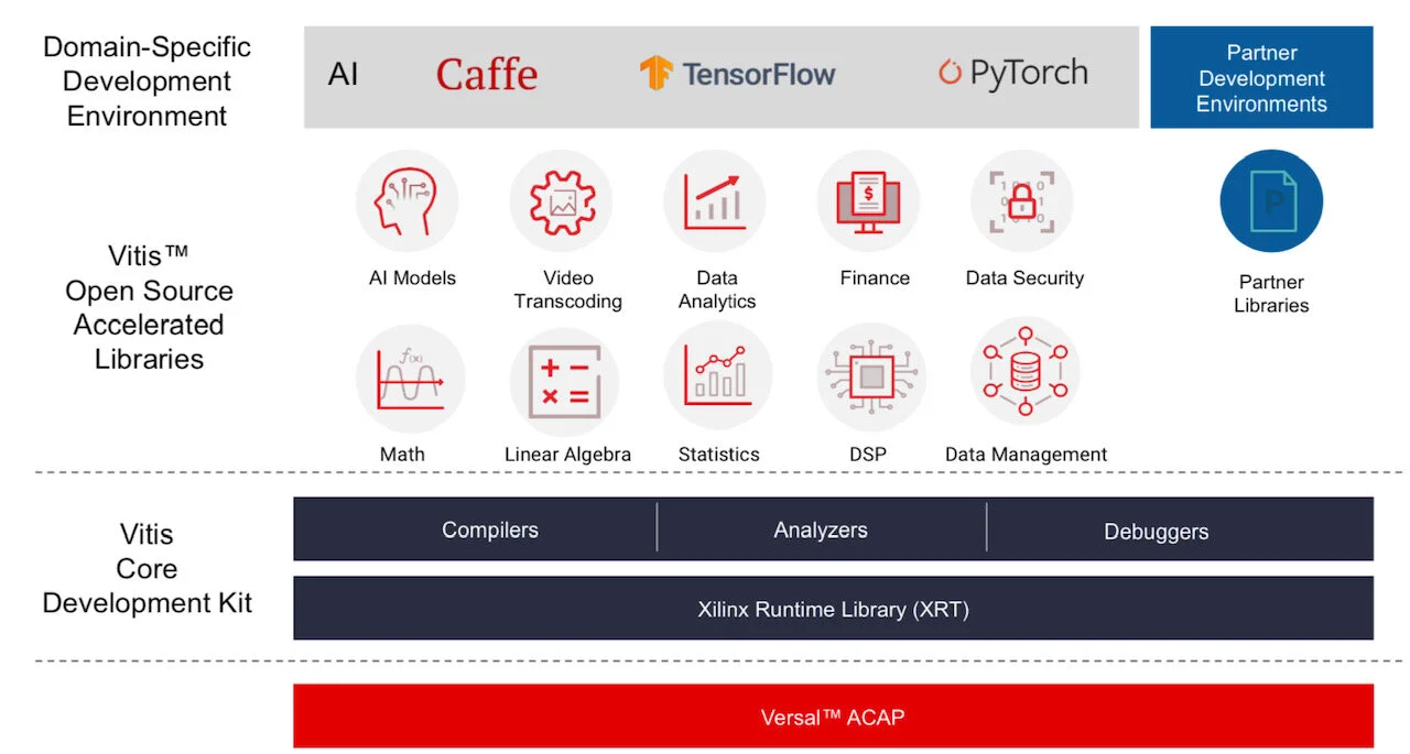
Vitis software tool. Source: Xilinx
Versal ACAPs come with advanced toolkit libraries so engineers can program the chip with no knowledge of the underlying hardware.
Xilinx is continuing to provide its Vivado toolset that supports register-transfer level (RTL), a design abstraction used by hardware engineers for their circuit designs. “The traditional RTL toolchain is not going away and will continue to evolve,” says Saban.
But coders developing data centre applications with no knowledge of RTL or programmable logic can now use Xilinx’s Vitis toolset that was launched in 2019.
“It is critical to enable software developers and data scientists doing machine learning a way to interface to our [ACAP] products,” says Saban.
Vitis supports programming languages such as C, C++ and Python as well as higher-level machine-learning frameworks such as TensorFlow and Caffe.
Xilinx also has a library of functions for tasks such as data analytics and genomics. Such applications can be switched in and out since they are executed using adaptive hardware.
The Premium software tools will be available in the fourth quarter of the year.
Lifespan
A programmable logic family’s lifespan is five or six years; the Virtex UltraScale family was launched in 2015.
“We added a few kickers [to the Virtex family] such as high bandwidth memory and 58-gigabit serdes,” says Saban. “And we will likely do the same with Versal, add some integrated block in a derivative product.”
Xilinx’s chip designers will likely now be already working on an ACAP architecture for 2026 supporting 1.6-terabit speeds and to be implemented using a 5nm CMOS process.
“If we are to deliver twice the bandwidth at half the power, it is not enough to lean on CMOS process technology,” says Saban. “We will need to look at new chip architectures to solve the problems.”
This is challenging. “It gets harder, it gets more expensive and there are less and fewer companies that can afford it,” says Saban.
Inphi unveils first 800-gigabit PAM-4 signal processing chip
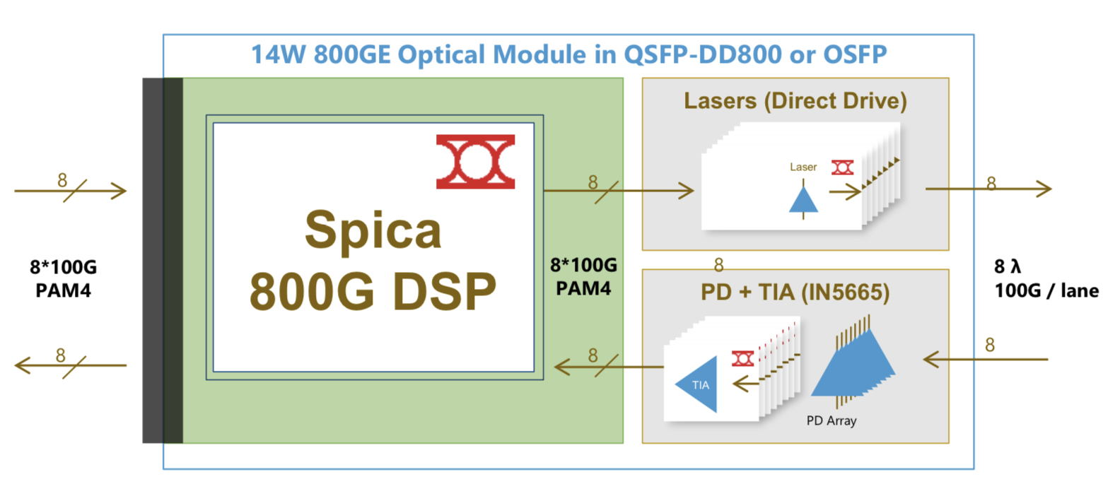
Inphi has detailed what it claims is the industry’s first digital signal processor (DSP) chip family for 800-gigabit client-side pluggable modules.
Dubbed Spica, the 4-level pulse-amplitude modulation (PAM-4) DSP family is sampling and is in the hands of customers.
The physical-layer company has also announced its third-generation Porrima family of PAM-4 DSPs for 400-gigabit pluggables.
The Porrima DSP with integrated laser driver has being made using a 7nm CMOS process; until now a 16nm CMOS has been used. Fabricating the chip using the more advanced process will reduce the power consumption of 400-gigabit module designs.
Applications
Eight-hundred-gigabit multi-source agreements (MSAs) will enable a new generation of high-speed optical transceivers to come to market.
The 800G Pluggable MSA developing optical specifications for 800-gigabit pluggable modules, is one that Inphi is promoting, while the QSFP-DD800 MSA is extending the double density form factor for 800 gigabits.

The main two markets driving a need for 800-gigabit modules are artificial intelligence (AI) and data centre switching, says Eric Hayes, senior vice president, networking interconnect at Inphi.
“AI, while still in its infancy, has all these applications and workloads that it can drive,” he says. “But one thing they have in common when we look at the data centres building large AI clusters is that they have very large data sets and lots of data flow.”
The speed of the input-output (I/O) of the AI processors used in the clusters is rising to cope with the data flows.
The second application that requires 800-gigabit modules is the advent of 25.6-terabit Ethernet switches used to network equipment within the data centre.
Inphi says there are two types of 25.6-terabit switch chips emerging: one uses 50-gigabit PAM-4 while the second uses 100-gigabit PAM-4 electrical interfaces.
“The 25.6-terabyte switch with 100-gigabit I/O is wanted for one-rack-unit (1RU) platforms,” says Hayes. “To do that, you need an 800-gigabit module.” Such switches have yet to reach the marketplace.
The first-generation AI processors used 25-gigabit non-return-to-zero (NRZ) signalling for the I/O while many of the devices shipping today use 50-gigabit PAM-4. “The latest designs that are coming to market have 100-gigabit I/O and we have the first DSP offering 100-gigabit on the host side,” says Hayes.
Spica and Porrima ICs
The Spica DSP takes 100-gigabits PAM-4 electrical signals from the host and performs retiming and pre-emphasis to generate the 100-gigabit PAM-4 signals used for modulation the optics before transmission. The laser driver is integrated on-chip.
The transmit path is a simpler design than the Porrima in that the signalling rate is the same at the input and the output. Accordingly, no gearbox circuitry is needed.
The main signal processing is performed at the receiver to recover the sent PAM-4 signals. A hybrid design is used combining analogue and digital signal processing, similar to the design used for the Porrima.
The Spica device supports 2×400-gigabit or 8×100-gigabit module designs and enables 800-gigabit or 8×100-gigabit optical interconnects. The 800-gigabit form factors used are the QSFP-DD800 and the OSFP. Inphi says both designs consume under 14W.
“The first module being built [using the Spica] is the OSFP because the end-user is demanding that, but we also have customers building QSFP-DDs,” says Hayes.
Meanwhile, Inphi’s Porrima family of devices is targeted at the 400G DR4 and 400G FR4 specifications as well as 100-gigabit module designs that use 100-gigabit PAM-4.
The two module types can even be combined when a 400-gigabit pluggable such as a QSFP-DD or an OSFP is used in breakout mode to feed four 100-gigabit modules implement using such form factors as the QSFP, uQSFP or SFP-DD.
Transitioning the Porrima to a 7nm process saves 1.5W of power, says Hayes, resulting in an 8W 400-gigabit module. The latest Porrima is sampling and is with customers.
Roadmap
Inphi says optical modules using the Spica DSP will be deployed in volume from the second half of 2021.
Before then, the DSP will be tested as part of customers’ module designs, then be integrated with the software before the complete 800-gigabit module is tested.
“There will then be interoperability testing between the modules once they become available and then small pilot networks using 800-gigabit modules will be built and tested before the go-ahead to mass deployment,” says Hayes.
All these stages will require at least a year’s work.
PCI Express back on track with latest specifications
Richard Solomon and Scott Knowlton are waiting for me in the lobby of a well-known Tel-Aviv hotel overseeing the sunlit Mediterranean Sea.
 Richard SolomonSolomon, vice chair of the PCI Special Interest Group (PCI-SIG), and Knowlton, its marketing working group co-chair, are visiting Israel to deliver a training event addressing the PCI Express (PCIe) high-speed serial bus standard.
With over 750 member companies, PCI-SIG conducts several training events around the world each year. The locations are chosen where there is a concentration of companies and engineers undertaking PCIe designs. “These are chip, board and systems architects,” says Solomon.
PCI-SIG has hit its stride after a prolonged quiet period. The group completed the PCIe 4.0 standard in 2017, seven years after it launched PCIe 3.0. The PCIe 4.0 doubles the serial bus speed and with the advent of PCIe 5.0, it will double again.
“We were late with PCIe 4.0,” admits Solomon. But with the introduction of the PCIe 5.0 standard in the first quarter of 2019, the serial bus’ speed progression will be back on track. “PCIe 5.0 is where the industry needs it to be.”
The latest training event is addressing the transition to PCIe 5.0. “User implementation stuff; the PHY, controller and verification IP,” says Knowlton. Verification IP refers to the protocols and interfaces needed to verify a PCIe 5.0-enabled chip design.
Markets
PCIe is used in a range of industries. In the cloud, the serial bus is used for servers and storage.
For servers, PCIe has been adopted by general-purpose microprocessors and more specialist devices such as FPGAs, graphics processing units and AI hardware.
The technology is also being used by enterprises, with PCIe switch silicon adopted in data centres to enable server redundancy and failover.
PCIe 5.0 is where the industry needs it to be
PCIe is also being used for storage and in particular solid-state drives (SSDs). That is because PCIe 4.0 transfers data at 16 gigabit-per-second (Gbps) per lane and can be scaled in parallel, typically in a by-four (x4) or a by-16 (x16) lane configuration.
The proportion of the SSDs that use PCIe is expected to grow from a quarter in 2018 to over three quarters in 2022, according to Forward Insights. Meanwhile, IDC forecasts that the SSD market will grow at a compound annual growth rate of 15 percent from 2016 to 2021.
PCIe is also employed within mobile handsets and for the Internet of Things designs. PCI-SIG attributes its adoption for these applications due to its speed and lane-width flexibility as well as its power efficiency.
 Source: PCI-SIG
Bus specifications
The PCIe bus uses point-to-point communications. The standard uses a simple duplex scheme - serial transmissions in both directions that is referred to as a lane. The bus can be bundled in a variety of lane configurations - x1, x2, x4, x8, x12, x16 and x32 - although x2, x12 and x32 are rarely, if ever, used in practice.
 Scott KnowltonThe first two iterations of PCIe, versions 1.0 and 2.0, delivered 2.5 and 5 gigatransfers-per-second (GT/s) per lane per direction, respectively.
A transfer refers to an encoded bit. The first two PCIe versions use an 8b/10b encoding scheme such that for every ten-bit payload sent, only 8 bits are data. This is why the data transfer rates per lane per direction are 2Gbps and 4Gbps (250 and 500 gigabytes-per-second), respectively (see table).
With PCIe 3.0, the decision was made to increase the transfer rate to 8GT/s per lane based on the assumption that no equalisation would be needed to counter inter-symbol interference at that speed, says Solomon. However, equalisation was needed in the end but that explains why PCIe 3.0 adopted 8GT/s and not 10GT/s.
Another PCIe 3.0 decision was to move to a 128b/130b scheme to reduce the encoding overhead from 20 percent to just over 1 percent. This is why the transfer rate and bit rate are almost equal from the PCIe 3.0 standard onwards (see table).
The recent PCIe 4.0 specification doubles the transfer rate from 8GT/s to 16GT/s while PCIe 5.0 will achieve 32GT/s per lane per direction.
When more than one lane is used, the encoded data is distributed across the lanes. A PCIe controller is used at each end of a lane to make sense of the bits. Meanwhile, a PCIe switch, a separate chip, can be used when fan out is needed to distribute the point-to-point links.
Compliance testing and design issues
Compliance testing of PCIe 4.0 will only occur in the beginning of 2019 even though it was standardised in 2017. Solomon says that this length of time is actually one of PCI-SIG's shorter periods. It takes time to refine the exact electrical testing to be used, he sys, and there is only so much that can be done until the silicon arrives.
Given that there are now 28Gbps and 56Gbps serialiser-deserialiser (serdes) technologies available, why were the PCIe 4.0 and PCIe 5.0 lane speeds not faster? Solomon says the latest PCIe standards were chosen to be multiples of the PCIe 3.0’s 8GT/s lane speed to ensure backward compatibility.
That said, designing systems using PCIe 4.0 and PCIe 5.0 signalling speeds is a challenge. Printed circuit boards need to be multi-layer and used higher-quality materials while retimer ICs are needed to achieve signal distances of 20 inches.
Solomon stresses that not all systems required such signal reaches; the dense electronics being developed for automotives that use AI techniques to make sense of their environment being one such example.
And with that, Solomon apologises and gets up: “I have a session to present”.