
Crossing oceans: Loi Nguyen's engineering odyssey

Loi Nguyen arrived in the US with nothing but determination and went on to co-found Inphi, a semiconductor company acquired by Marvell for $10 billion. Now, the renowned high-speed semiconductor entrepreneur is ready for his next chapter.
“What is the timeline?”
It’s a question the CEO of Marvell, Matt Murphy, would pose to Loi Nguyen each year during their one-on-one meetings. “I’ve always thought of myself as a young guy; retirement seemed far away,” says Nguyen. “Then, in October, it seemed like the time is now.”
Nguyen will not, however, disappear. He will work on specific projects and take part in events, but this will no longer be a full-time role.
Early life and journey to the US
One of nine children, Nguyen grew up in Ho Chi Minh City, Vietnam. Mathematically inclined from an early age, he faced limited options when considering higher education.
“In the 1970s, you could only apply to one university, and you either passed or failed,” he says. “That decided your career.”
Study choices were also limited, either engineering or physics. Nguyen chose physics, believing entrance would be easier.
After just one year at university, he joined the thousands of ‘boat people’ that left Vietnam by sea following the end of the Vietnam War in 1975.
But that one year at university was pivotal. “It proved I could get into a very tough competitive environment,” he says. “I could compete with the best.”
Nguyen arrived in the US with limited English and no money. He found work in his first year before signing up at a community college. Here, he excelled and graduated with first-class honours.
Finding a mentor & purpose
Nguyen’s next achievement was to gain a full scholarship to study at Cornell University. At Cornell, Nguyen planned to earn his degree, find a job, and support his family in Vietnam. Then a Cornell academic changed everything.
The late Professor Lester Eastman was a pioneer researcher in high-speed semiconductor devices and circuits using materials such as gallium arsenide and indium phosphide. “Field-effect transistors (FETs), bipolar – any kind of high-speed devices,” says Nguyen. “I was just so inspired by how he talked about his research.”
In his senior year, Nguyen talked to his classmates about their plans. Most students sought industry jobs, but the best students were advancing to graduate school.
“What is graduate school?” Nguyen asked and was told about gaining a doctorate. “How one does that?” he asked and was told about the US Graduate Record Examination (GRE). “I hadn’t a clue,” he says.
The GRE deadline to apply to top US universities was only a week away, including an exam. Nguyen passed. He could now pursue a doctorate at leading US universities, but he chose to stay at Cornell under Professor Eastman: “I wanted to do high-speed semiconductors.”
His PhD addressed gallium arsenide FETs, which became the basis for today’s satellite communications.
Early career breakthroughs
After graduating, he worked for a satellite company focussing on low-noise amplifiers. NASA used some of the work for a remote sensing satellite to study cosmic microwave background radiation. “We were making what was considered the most sensitive low-noise receivers ever,” says Nguyen.
However, the work concluded in the early 1990s, a period of defence and research budget cuts. “I got bored and wondered what to do next,” he says.
Nguyen’s expertise was in specialised compound semiconductor devices, whereas CMOS was the dominant process technology for chip designs. He decided to undertake an MBA, which led to his co-founding the high-speed communications chip company Inphi.
While studying for his MBA, he met Tim Semones, another Inphi co-founder. The third co-founder was Gopal Raghavan whom Nguyen describes as a classic genius: “The guy could do anything.”
Building Inphi: innovation through persistence
The late 1990s internet boom created the perfect environment for a semiconductor start-up. Nguyen, Semones, and Raghavan raised $12 million to found Inphi, shorthand for indium phosphide.
The company’s first decade was focused on analogue and mixed-signal design. The market used 10-gigabit optics, so Inphi focused on 40 gigabits. But then the whole optical market collapsed, and the company had to repurpose.
Inphi went from designing indium phosphide chips at 40 gigabits-per-second (Gbps) to CMOS process circuits for memory working at 400 megabits-per-second (Mbps).
In 2007, AT&T started to deploy 40Gbps, indicating that the optical market was returning. Nguyen asked the chairman for a small team which subsequently developed components such as trans-impedance amplifiers and drivers. Inphi was too late for 40Gbps, so it focussed on chips for 100Gbps coherent optics.
Inphi also identified the emerging cloud data centre opportunity for optics. Initially, Nguyen considered whether 100Gbps coherent optics could be adopted within the data centre. However, coherent was too fast and costly compared to traditional non-return-to-zero (NRZ) signalling-based optics.
It led to Inphi developing a 4-level pulse-amplitude modulation (PAM4) chip. Nguyen says that, at the time, he didn’t know of PAM4 but understood that Inphi needed to develop technology that supported higher-order modulation schemes.
“We had no customer, so we had to spend our own money to develop the first PAM4 chip,” says Nguyen.
Nguyen also led another Inphi group in developing an in-house silicon photonics design capability.
These two core technologies – silicon photonics and PAM4 – would prove key in Inphi’s fortunes and gain the company a key design win with hyperscaler Microsoft with the COLORZ optical module.
Microsoft met Inphi staff at a show and described wanting a 100Gbps optical module that could operate over 80km to link data centre sites yet would consume under 3.5W. No design had done that before.
Inphi had PAM4 and silicon photonics by then and worked with Microsoft for a year to make it happen. “That’s how innovation happens; give engineers a good problem, and they figure out how to solve it,” says Nguyen.

Marvell transformation
The COVID-19 pandemic created unlikely opportunities. Marvell’s CEO, Matt Murphy, and then-Inphi CEO, Ford Tamer, served on the Semiconductor Industry Association (SIA) board together. It led to them discussing a potential acquisition during hikes in the summer of 2020 when offices were closed. By 2021, Marvell acquired Inphi for $10 billion.
“Matt asked me to stay on to help with the transition,” says Nguyen. “I knew that for the transition to be successful, I could play a key role as an Inphi co-founder.”
Nguyen was promoted to manage most of the Inphi optical portfolio and Marvell’s copper physical layer portfolio.
“Matt runs a much bigger company, and he has very well thought-out measurement processes that he runs throughout the year,” he says. “It is one of those things that I needed to learn: how to do things differently.”
The change as part of Marvell was welcome. “It invigorated me and asked me to take stock of who I am and what skills I bring to the table,” says Nguyen.
AI and connectivity
After helping ensure a successful merger integration, Nguyen returned to his engineering roots, focusing on optical connectivity for AI. By studying how companies like Nvidia, Google, and Amazon architect their networks, he gained insights into future infrastructure needs.
“You can figure out roughly how many layers of switching they will need for this and the ratio between optical interconnect and the GPU, TPU or xPU,” he says. “Those are things that are super useful.”
Nguyen says there are two “buckets” to consider: scale-up and scale-out networks. Scale-out is needed when connecting 10,000s, 100,000 and, in the future, 1 million xPUs via network interface cards. Scale-out networks use protocols such as Infiniband or Ethernet that minimise and handle packet loss.
Scale-up refers to the interconnect between xPUs in a very high bandwidth, low latency network. This more local network allows the xPUs to share each other’s memory. Here, copper is used: it is cheap and reliable. “Everyone loves copper,” says Nguyen. But copper’s limitation is reach, which keeps shrinking as signalling speeds increase.
“At 200 gigabits, if you go outside the rack, optics is needed,” he says. “So next-gen scale-up represents a massive opportunity for optics,” he says.
Nguyen notes that scale-up and scale-out grow in tandem. It was eight xPUs in a scale-up for up to a 25,000 xPU scale-out network cluster. Now, it is 72 xPUs scale-up for a 100,000 xPU cluster. This trend will continue.
Beyond Technology
Nguyen’s passion for wildlife photography is due to his wife. Some 30 years ago, he and his wife supported the reintroduction of wolves to the Yellowstone national Park in the US.
After Inphi’s initial public offering (IPO) in 2010, Nguyen could donate money to defend wildlife, and he and his wife were invited to a VIP retreat there.
“I just fell in love with the place and started taking up photography,” he says. Though initially frustrated by elusive wolves, his characteristic determination took over. “The thing about me is that if I’m into something, I want to be the best at it. I don’t dabble in things,” he says, laughing. “I’m very obsessive about what I want to spend my time on.
He has travelled widely to pursue his passion, taking what have proved to be award-winning photos.
Full Circle: becoming a role model
Perhaps most meaningful in Nguyen’s next chapter is his commitment to Vietnam, where he’s been embraced as a high-tech role model and a national hero.
He plans to encourage young people to pursue engineering careers and develop Vietnam’s high-speed semiconductor industry, completing a circle that began with his departure decades ago.
He also wants to spend time with his wife and family, including going on an African safari.
He won’t miss back-to-back Zoom calls and evenings away from home. In the last two years, he estimates that he has been away from home between 60 and 70 per cent of the time.
It seems retirement isn’t an ending but a new beginning.

Steve Alexander's 30-Year Journey at Ciena
After three decades of shaping optical networking technology, Steve Alexander is stepping down as Ciena’s Chief Technology Officer (CTO).
His journey, from working on early optical networking systems to helping to implement AI as part of Ciena’s products, mirrors the evolution of telecommunications itself.
The farewell
“As soon as you say, ‘Hey guys, you know, there’s an end date’, certain things start moving,” says Alexander reflecting on his current transition period. “Some people want to say goodbye, others want more of your time.”
After 30 years of work, the bulk of it as CTO, Alexander is ready to reclaim his time, starting with the symbolic act of shutting down Microsoft Outlook.
“I don’t want to get up at six o’clock and look at my email and calendar to figure out my day,” he says.
His retirement plans blend the practical and the fun. The agenda includes long-delayed home projects and traveling with his wife. “My kids gave us dancing lessons for a Christmas present, that sort of thing,” he says with a smile.
Career journey
The emergence of the erbium-doped fibre amplifier shaped Alexander’s career.
The innovation sparked the US DARPA’s (Defense Advanced Research Projects Agency) interest in exploring all-optical networks, leading to a consortium of AT&T, Digital Equipment Corp., and MIT Lincoln Labs, where Alexander was making his mark.
“I did coherent in the late 80s and early 90s, way before coherent was cool,” he recalls. The consortium developed a 20-channel wavelength division multiplexing (WDM) test bed, though data rates were limited to around 1 Gigabit-per-second due to technology constraints.
“It was all research with components built by PhD students, but the benefits for the optical network were pretty clear,” he says.
The question was how to scale the technology and make it commercial.
A venture capitalist’s tip about a start-up working on optical amplifiers for cable TV led Alexander to Ciena in 1994, where he became employee number 12.
His first role was to help build the optical amplifier. “I ended up doing what effectively was the first kind of end-to-end link budget system design,” says Alexander. “The company produced its first product, took it out into the industry, and it’s been a great result since.”
The CTO role
Alexander became the CTO at Ciena at the end of the 1990s.
A CTO needs to have a technology and architecture mindset, he says, and highlights three elements in particular.
The first includes such characteristics as education and experience, curiosity, and imagination. Education is essential, but over time, it is interchangeable with experience. “They are fungible,” says Alexander.
Another aspect is curiosity, the desire to know how things work and why things are the way they are. Imagination refers to the ability to envisage something different from what it is now.
“One of the nicest things about the engineering skill set, whatever the field of engineering you’re in, is that with the right tools and team of people, once you have the idea, you can make it happen,” says Alexander.
Other aspects of the CTO’s role are talking, travelling, trouble-making, and tantrum throwing. “Trouble-making comes from the imagination and curiosity, wanting to do things maybe a little bit different than the status quo,” says Alexander.
And tantrums? “When things get really bad, and you just have to make a change, and you stomp your foot and pound the table,” says Alexander.
The third aspect a CTO needs is being in the “crow’s nest”, the structure at the top of a ship’s mast: “The guy looking out to figure out what’s coming: is it an opportunity? A threat? And how do we navigate around it,” says Alexander.
Technology and business model evolution
Alexander’s technological scope has grown over time, coinciding with the company’s expanding reach to include optical access and its Blue Planet unit.
“One of the reasons I stayed at the company for 30 years is that it has required a constant refresh,” says Alexander. “It’s a challenge because technology expands and goes faster and faster.”
His tenure saw the transformation from single-channel Sonet/ SDH to 16-channel WDM systems. But Alexander emphasizes that capacity wasn’t the only challenge.
“It’s not just delivering more capacity to more places, the business model of the service providers relies on more and more levels of intelligence to make it usable,” he says.
The gap between cloud operators’ agility and that of the traditional service providers became evident during Covid-19. “The reason we’re so interested in software and Blue Planet is changing that pretty big gap between the speed at which the cloud can operate and the speed at which the service provider can operate.”
Coherent optics
Ciena is shipping the highest symbol rate coherent modem, the WaveLogic 6 Extreme. This modem operates at up to 200 gigabaud and can send 1.6 terabits of data over a single carrier.
Alexander says coherent optics will continue to improve in terms of baud rate and optical performance. But he wonders about the desired direction the industry will take.
He marvels at the success of Ethernet whereas optical communications still has much to do in terms of standardization and interoperability.
There’s been tremendous progress by the OIF and initiatives such as 400ZR, says Alexander: “We are way better off than we were 10 years ago, but we’re still not at the point where it’s as ubiquitous and standardised as Ethernet.”
Such standardisation is key because it drives down cost.
“People have discussed getting on those Ethernet cost curves from the photonic side for years. But that is still a big hurdle in front of us,” he says.
AI’s growing impact
It is still early days for AI, says Alexander, but there are already glimmers of success. Longer term, the impact will likely be huge.
AI is already having an impact on software development and on network operations.
Ciena’s customers have started by looking to do simple things with AI, such as reconciling databases. Service providers have many such data stores: an inventory database, a customer database, a sales database, and a trouble ticket database.
“Sometimes you have a phone number here, an email there, a name elsewhere, things like a component ID, all these different things,” he says. ”If you can get all that reconciled into a consistent source of knowledge, that’s a huge benefit.”
Automation is another area that typically requires using multiple manual systems. There are also research papers appearing where AI is being used to design photonic components delivering novel optical performance.
AI will also impact the network. Humans may still be the drivers but it will be machines that do the bulk of the work and drive traffic.
“If you are going to centralize learning and distributed inferencing, it’s going to have to be closer to the end user,” says Alexander.
He uses a sports application as an example as to what could happen.
“If you’re a big soccer/ football fan, and you want to see every goal scored in every game that was broadcast anywhere in the world in the last 24 hours, ranked in a top-10 best goals listing, that’s an interesting task to give to a machine,” he says.
Such applications will demand unprecedented network capabilities. Data will need to be collected, and there will be a lot of machine-to-machine interactions to generate maybe a 10-minute video to watch.
“If you play those sorts of scenarios out, you can convince yourself that yes, networks are going to have lots of demand placed on them.”
Personal Reflection
While Alexander won’t miss his early morning Outlook checks, he’ll miss his colleagues and the laboratory environment.
A Ciena colleague, paying tribute to Alexander, describes him as being an important steward of Ciena’s culture. “He always has lived by the credo that if you care for your people, people will care for the company,” he says.
Alexander plans to keep up with technology developments, but he acknowledges that losing the inside view of innovation will be a significant change.
When people have asked him why he has stayed at Ciena, his always has answered the same way: “I joined Ciena for the technology but I stayed because of the people.”
Further Information
Ciena’s own tribute, click here

Podcast: Is AI driving a new wave of photonic innovation?

AI is still in its infancy, but it’s already pushing the photonics and computing industries to rethink product roadmaps and drive new levels of innovation.
Adtran’s Gareth Spence talks with authors and analysts Daryl Inniss and the editor of Gazettabyte about the fast pace of AI development and the changes needed to unlock its full potential. They also discuss the upcoming sequel to their book on silicon photonics and its focus on AI.
To listen to the podcast, click here.

Is network traffic growth dwindling to a trickle?
“Network capacities are sufficient, and with data usage expected to plateau in the coming years, further capacity expansion is not needed. We have reached the end of history for communications.”
– Willian Webb, The End of Telecoms History
William Webb has pedigree when it comes to foreseeing telecoms trends.
Webb wrote The 5G Myth in 2016, warning that 5G would be a flop.
In the book, he argued that the wireless standard’s features would create limited interest and fail to grow revenues for mobile operators.

The next seven years saw the telcos promoting 5G and its capabilities. Now, they admit their considerable investments in 5G have delivered underwhelming returns.
His latest book, The End of Telecoms History, argues that telecoms has reached a maturity that satisfies the link speeds needed and that traffic growth is slowing.
“There will be no end of new applications,” says Webb. “But they won’t result in material growth in data requirements or in data speeds.”
What then remains for the telcos is filling in the gaps to provide connectivity everywhere.
Traffic growth slowdown
Earlier this year, AT&T’s CEO, John Stankey, mentioned that its traffic had grown 30 per cent year over year, the third consecutive year of such growth for the telco. The 30 per cent annual figure is the typical traffic growth rate that has been reported for years.
“My take is that we are at about 20 per cent a year annual growth rate worldwide, and it’s falling consistently by about 5 per cent a year,” says Webb.
In 2022, yearly traffic growth was 30 per cent; last year, it was 25 per cent. These are the average growth rates, notes Webb, and there are enormous differences worldwide.
“I was just looking at some data and Greece grew 45 per cent whereas Bahrain declined 10 per cent,” says Webb. “Clearly, there will be big differences between operators.”
He also cites mobile data growth numbers from systems vendor Ericsson. In North America, the growth between 2022 and 2024 was 24 per cent, 17 per cent, and 26 per cent.
“So it is fluctuating around the 20 per cent mark,” says Webb.
Other developments
What about trends like the ever-greater use of digital technologies experienced by many industries, including telecoms? Or the advent of artificial intelligence (AI), which is leading to significant data centre builds, and how AI is expected to change traffic?
“If you look at all non-personal data use, such as the Internet of Things and so on, traffic levels are tiny,” says Webb. There are exceptions, such as security cameras generating video streams. “I don’t see that trend materially changing overall data rates,” says Webb.
He also doesn’t see AI meaningfully growing overall traffic. AI is useful for improving the running of networks but not changing the amount of wireless traffic. “If anything, it might reduce it because you can be more intelligent about what you need to send,” he says.
While Webb admits that AI data centre builds will require extra fixed networking capacity, as will sharing workloads over distributed data centres in a metropolitan area, he argues that this represents a tiny part of the overall network.
He does not see any new devices emerging that will replace the smartphone, dramatically changing how we consume and interact with data.
5G and 6G
Webb also has doubts about the emerging 6G wireless standard. The academic community is busy developing new capabilities for the next wireless standard. “The problem with that is that academics are generally not grounded in the reality of what will make money in the future,” says Webb. Instead, developers should challenge academics to develop the technologies needed for their applications to succeed.
Webbs sees two 6G camps emerging. The first camp wants 6G to address all the shortfalls of 5G using terahertz frequencies and delivering hundreds of gigabits speeds.
“Let’s max out on everything, and then surely, something wonderful must happen,” says Webb. “This strikes me as not learning the lessons of 5G.”
The second camp, including several telcos, does not want to spend any money on 6G but instead wants the technology, in the form of software updates, to address high operational costs and the difficulties in running different network types.
“In this case, 6G improves the operator’s economics rather than improve the end-user offering, which I think makes sense,” says Webb.
“We may end up in a situation where 6G has all this wondrous stuff, and the operators turn around and say they are not interested,” says Webb. “I see a significant risk for 6G, that it just isn’t ever really deployed anywhere.”
Webb’s career in telecoms spans 35 years. His PhD addressed modulation schemes for radio communications. He spent seven years at the UK regulator Ofcom addressing radio spectrum strategy, and he has also been President of the IET, the UK’s equivalent of the IEEE. Webb also co-founded an IoT startup that Huawei bought. For the last 15 years, he has been a consultant covering telecom strategy and technology.
Outlook
The dwindling growth in traffic will impact the telecom industry.
Webb believes the telcos’ revenues will remain the same resulting in somewhat profitable businesses. “They’re making more profit than utilities but less than technology companies,” says Webb.
He also expects there will be more mergers, an obvious reaction to a market flattening out. The aim is to improve profitability.
Given his regulatory background, is that likely? Regulators shun consolidation as they want to keep competition high. He expects it to happen indirectly, with telcos increasingly sharing networks. Each market will offer three or four brands for consumers per market but fewer networks; operators merging in all but name.
Will there even be a need for telecom consultants? “I have to say, as I’ve made these predictions, I’ve been thinking what am I needed for now?” says Webb, laughing.
If he is right, the industry will be going through a period of change.
But if the focus becomes extending connectivity everywhere, there is work to be done in understanding and addressing the regulatory considerations, and also how best to transition the industry.
“I do suspect that just as the rest of the industry is effectively more a utility, it will need fewer and fewer consultants,” he says.

Will AI spur revenue growth for the telcos?
- A global AI survey sponsored by Ciena highlights industry optimism
- The telcos have unique networking assets that can serve users of AI.
- Much is still to play out and telcos have a history of missed opportunities.
The leading communications service providers have been on a decade-long journey to transform their networks and grow their revenues.
To the list of technologies the operators have been embracing can now be added artificial intelligence (AI).
AI is a powerful tool for improving their business efficiency. The technology is also a revenue opportunity and service providers are studying how AI traffic will impact their networks.
“This is the single biggest question that everyone in this industry is struggling with,” says Jürgen Hatheier. “How can the service providers exploit the technology to grow revenues?”
However, some question whether AI will be an telecom opportunity.
“The current hype around AI has very little to do with telcos and is focused on hyperscalers and specifically the intra-data centre traffic driven by AI model training,” says Sterling Perrin, senior principal analyst at HeavyReading. “There is a lot of speculation that, ultimately, this traffic will spread beyond the data centre to data centre interconnect (DCI) applications. But there are too many unknowns right now.”
AI survey
Hatheier is chief technology officer, international at Ciena. He oversees 30 staff, spanning Dublin to New Zealand, that work with the operators to understand their mid- to long-term goals.
Ciena recently undertook a global survey (see note 1, bottom) about AI, similar to one it conducted two years ago that looked at the Metaverse.
Conducting such surveys complements Ciena’s direct research with the service providers. However, there is only so much time a telco’s chief strategy officer (CSO) or chief technology officer (CTO) can spend with a vendor discussing strategy, vision, and industry trends.
“The survey helps confirm what we are hearing from a smaller set,” says Hatheier.
Surveys also uncover industry and regional nuances. Hatheier cites how sometimes it is the tier-two communications service providers are the trailblazers.
Lastly, telcos have their own pace. “It takes time to implement new services and change the underlying network architecture,” says Hatheier. “So it is good to plan.”

Findings
The sectors expected to generate the most AI traffic are financial services (46 per cent of those surveyed), media and entertainment (43 per cent), and manufacturing (38 per cent). Hatheier says these industries have already been using the technology for a while, so AI is not new to them.
Sterling Perrin
For financial services, an everyday use of AI is for security, detecting fraudulent transactions and monitoring video streams to detect anomalous behavior at a site. The amount of traffic AI applications generate can vary greatly. This is common, says Hatheier; it is the use that matters here, not the industry.
“I would not break it down by the industries to say, okay, this industry is going to create more traffic than another,” says Hatheier. “For financial services, if it is transaction data, it’s a few lines of text, but if it is video for branch security, the data volumes are far more significant.”
AI is also set to change the media and entertainment sector, challenging the way content is consumed. Video streaming uses content delivery networks (CDNs) to store the most popular video content close to users. But AI promises to enable more personalised video, tailored for the end-user. Such content will make the traffic more dynamic.
Another example of personalised content is for marketing and advertising. Such personalisation tends to achieve better results, says Hatheier.
AI is also being applied in the manufacturing sector. Examples include automating supply-chain operations, predictive maintenance, and quality assurance.
Car manufacturers check a vehicle for any blemishes at the end of a production line. This usually takes several staff and lasts 10-15 minutes. Now with AI, the inspection can be completed as the cars passes by. “This is a potent application that could run on infrastructure within the manufacturing site but use a service provider’s compute assets and connectivity,” says Hatheier.
The example shows how AI produces productivity gains. However, AI also promises unique abilities that staff cannot match.

Traffic trends
If the history of telecoms is anything to go by, applications that drove traffic in the network rarely lead to revenue growth for the service providers. Hatheier cites streaming video, gaming, and augmented reality as examples.
However, the operators have assets at network edge and the metro that can benefit AI usage. They also have central offices that can act is distributed data centres for the metro and network edge.
Hatheier says users have an advantage if they consume AI applications across a fibre-based broadband network. But certain countries, such as Saudi Arabia and India, mainly use wireless for connectivity.
“AI applications will need to adapt to what is available, and if people want to consume low-latency applications, there is 5G slicing,” says Hatheier. “At the end of the day, there is no way around fibre.”
Optical networking
Government policy regarding AI and regulations to ensure data does not cross borders also play a part.
“It’s an important decision criterion, as we saw in the survey response,” says Hatheier. “So private AI and local computing will be an important decision factor.”
Another critical decision influencing where data centres are built is power. “We see all the gold rush in the Nordics right now with their renewable power and cool climates,” says Hatheier. “You don’t need to cool your servers as much, and it requires a lot of connectivity.”
However, as well as these region-specific data centre builds, there will also be builds in metropolitan areas using smaller distributed data centres.
“Let’s say there are 20 sizable edge or metro compute centres for AI, and you would need three or four to run a big training job,” says Hatheier. “You will not create a permanent end-to-end connection between them because sometimes there will not be four that need to work together, but five, seven, and 11.”
Such a metro network would require reconfigurable optical add-drop multiplexer (ROADM) technology to connect wavelengths between those clusters based on demand to keep sites busy, to avoid expensive AI clusters being idle.
These are opportunities for the CSPs. And while much is still to happen, such discussions are taking place between systems vendors and the telcos.
For Heavy Reading’s Perrin, the more telling opportunity is the telcos’ own use of AI rather than the networking opportunity.
“As a vertical industry, telecom is not typically a leading-edge adopter of any new technology due to many factors, including culture, size, legacy infrastructure and processes, and government regulations,” he says. “I don’t believe AI will be any different.”
Hatheier points to the survey’s finding of general optimism that sees AI as an opportunity rather than a challenge or business risk.
“We have seen very little differences between countries,” says Hatheier. “That may have to do with the fact that emerging countries get as much attention of data centre investment than more developed ones.”

Cloud and AI: Opportunities that must be grabbed
The founder of Cloud Light, Dennis Tong, talks about the company, how its sale to Lumentum came about, and the promise of cloud and AI markets for optics.

For Dennis Tong (pictured), Hong Kong is a unique place that has a perfect blend of the East and West.
Tong, the founder and CEO of optical module specialist Cloud Light, should know. The company is headquartered in Hong Kong and has R&D offices in Hong Kong and Taipei, Taiwan. Cloud Light also has manufacturing sites in Asia: in the Chinese city of Dongguan—two hours by car, north of Hong Kong—and in the Philippines.
Now, Cloud Light is part of Lumentum. The U.S. photonics firm bought the optical module maker for $750 million in November 2023.
Tie-up
Cloud Light is a volume manufacturer of optical modules. The company takes 12-inch silicon photonic wafers, tests the wafers’ dies, and packages them for use in optical modules.
Cloud Light has a long relationship with Lumentum, using the U.S. company’s continuous-wave lasers for its silicon photonic-based optical modules.
Tong says he has been in photonics for 30 years and has good friends at Lumentum. “We had opportunities to chat and exchange views as to where the industry is going, and we shared a common vision,” he says. Eventually, the talk turned to a possible merger and acquisition.
Tong says the decision to sell the company centred on how best to grow the company. Cloud Light would have continued to do well, he says, but the company could grow much faster if he and his 1,600 staff joined Lumentum.
It is also timely. “Opportunities such as cloud and AI, they don’t come along very often,” says Tong.

Wafer-in, Product-out
Cloud Light has developed a manufacturing process dubbed “wafer-in, product-out.”
Turning a photonic integrated circuit (PIC) into a packaged optical module involves many stages and players. Designers of a PIC pass it to a foundry that results in the wafer. The wafer is shipped to an outsourced semiconductor assembly and test (OSAT) that does wafer back-end tasks: testing and dicing the wafer, and polishing. The working PICs—the known good dies—are shipped to a contract manufacturer that makes the pluggable modules.
“You can see that the entire collaboration chain is fragmented,” says Tong. “With our wafer-in, product-out process, we put everything in one group.”
Cloud Light takes the wafer from the foundry and does all the steps resulting in the delivered module.
Tong says the advantage of undertaking the complete process includes improved product yield. For example, the company measures coupling loss to the PIC and its optical waveguide loss during testing, and uses the insight to improve product yield.
Cloud Light has developed its own equipment to support automation. This know-how means that its design staff can work with the process and equipment colleagues to tailor the manufacturing process for new product designs. The precise assembly of unique micro-optics is one example.
It is this expertise and capability that particularly interested Lumentum in Cloud Light.
According to Tong, accumulating expertise in the different production areas has taken years: “There is a lot of subtlety to it, and we started to set this up in 2017.”
Hyperscaler business
Cloud Light succeeded early with a hyperscaler, making a 4×10-gigabit multimode VCSEL-based transceiver. But it soon realised market growth was coming from single-mode optical transceivers.
Its decision to pursue its wafer-in, product-out strategy stemmed from a desire to avoid becoming one of many single-mode optical transceiver makers. “We didn’t think we would add any value to the market by just creating a me-too company,” says Tong.
If the company was going to invest in a new platform, it would have to be scalable to support high volumes.
“It was very clear that silicon photonics was the right thing to do,” says Tong. “We were one of the first, if not the first, to launch a 400-gigabit silicon photonics-based transceiver in 2019.”
Cloud Light pitched its in-house scalable manufacturing approach to a hyperscaler that liked its plan, resulting in the company securing the hyperscaler as a customer.
Plans
Since the acquisition’s completion, Lumentum has given Cloud Light broad scope; there is no rush for full-blown integration, says Tong.
“Our mandate is to continue to grow the module business,” he says. “And we are open to using components from Lumentum and other suppliers.”
Lumentum’s components also offer Cloud Light the ability to create new products. “Customers are seeing us as more equipped, which opens up new, interesting opportunities,” says Tong.
Moreover, Cloud Light is not solely making modules for Lumentum. “The reality is that this is a very dynamic market, dominated by a few customers,” says Tong. “We are open to different business models as long as we can add value.”
Opportunities
At the time of the deal, Lumentum revealed that it expected Cloud Light would add $200 million plus to its yearly income. Cloud Light’s $200 million in revenues in the previous year was almost all from 400-gigabit and higher-speed transceiver sales.
Lumentum also makes coherent optical modems, ROADMs, and 3D sensing for commercial applications. Tong says coherent modules are one obvious opportunity for Cloud Light: “If you look into the future, I think the line between cloud/ datacom and telecom will become blurred.”
Cloud and AI will drive volumes, and the silicon photonics platform will be applicable for coherent modems as well. “So, a lot of the things that we have developed will also be applicable to coherent modules in the future,” says Tong. “And it is definitely applicable if one day coherent optics makes its way into the data centre.”
Coherent optics modules will keep increasing symbol rate and use more sophisticated coding schemes, but at some point, the effective data rate per line will start to plateau. To increase bandwidth beyond that, designs will go parallel by adding more channels. “Adding more fibre or more wavelengths, then it comes back to density, and then it’s all about packaging,” says Tong.
The ability to change its automated assembly for new applications also suggests that Cloud Light’s manufacturing capability could benefit Lumentum’s other product lines, such as ROADMs and even new markets such as optical circuit switches.
Co-packaged optics
Co-packaged optics are seen as one solution for applications where standard pluggable optics are no longer suitable.
Tong says that there are still issues before co-packaged optics are deployed at scale. One challenge is reliability; hyperscalars will not deploy the technology at scale until it has demonstrable good quality and reliability.
“The emergence of AI and cloud may accelerate that deployment, simply because of the volumes they are using and the density issue,” says Tong. Cost and thermal issues is also something co-packaged optics can address.
Cloud Light is ready for the advent of co-packaged optics. For its 800-gigabit transceiver, it can package a bare-die digital signal processor right next to the silicon photonics optical engine. “It’s not exactly a co-packaged optics product, but it has the same capability,” he says.
Shrinking lifecycles
The lifecycle of optical module products continues to shrink. At 10 gigabits, it was a decade-plus; for 100 gigabits, it was five to six years; at 400 gigabits, it has been more like three or four years. “Now, with AI, it is more like two to three years,” says Tong.
To be successful, it is all about time-to-market and time-to-scale.
“You need to be able to ramp up very quickly to the type of volumes and the type of quality that the customer is asking for,” says Tong. “There’s no time for you to get ready; you must be ready.”

Broadcoms taps AI to improve switch chip traffic analysis
Broadcom’s Trident 5-X12 networking chip is the company’s first to add an artificial intelligence (AI) inferencing engine.
Data centre operators can use their network traffic to train the chip’s neural network. The Trident 5’s inference engine, dubbed the Networking General-purpose Neural-network Traffic-analyzer or NetGNT, is loaded with the resulting trained model to classify traffic and detect security threats.
“It is the first time we have put a neural network focused on traffic analysis into a chip,” says Robin Grindley, principal product line manager with Broadcom’s Core Switching Group.
Adding an inference engine shows how AI can complement traditional computation, in this case, packet processing.
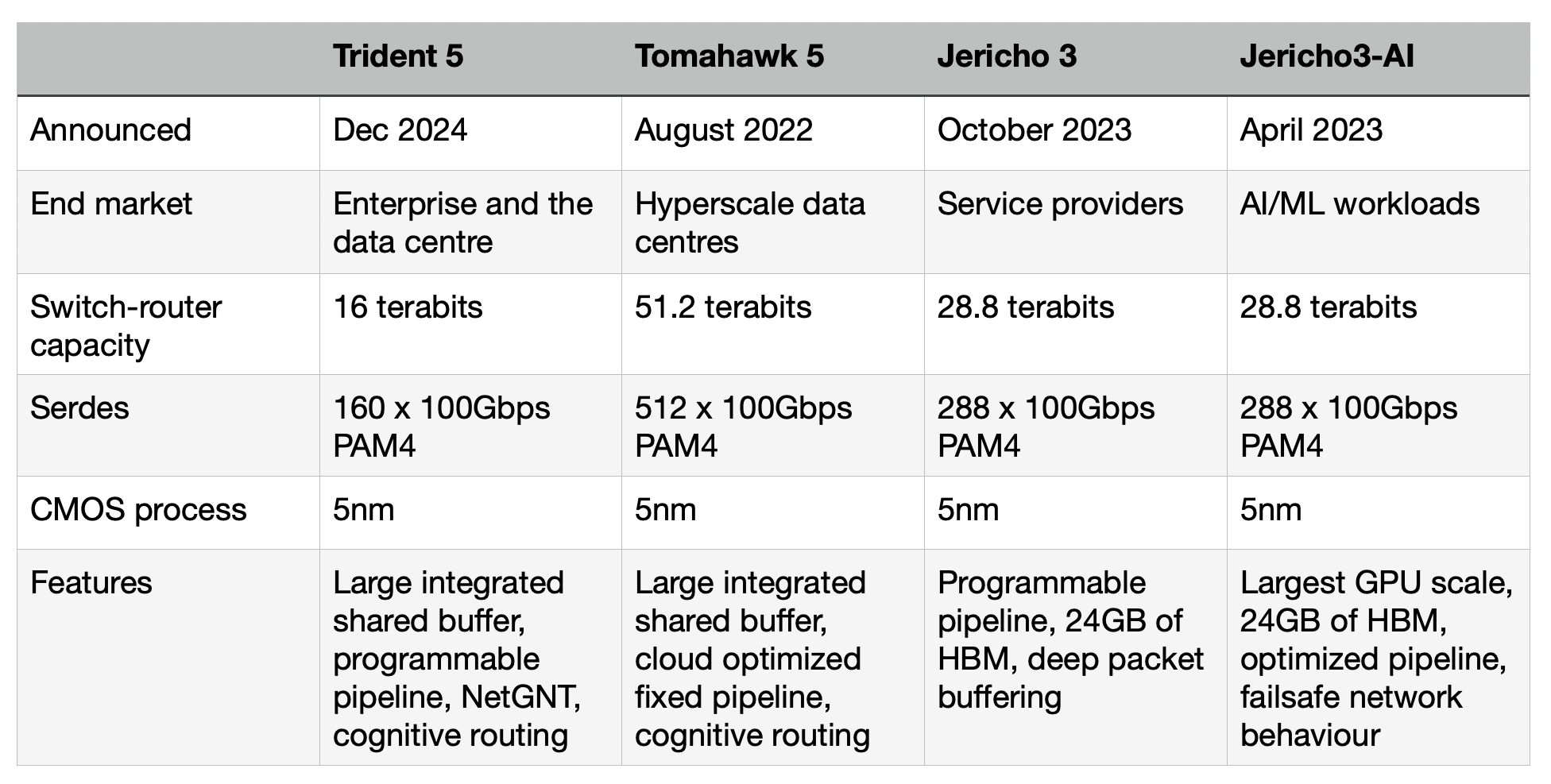
Trident family
Trident is one of Broadcom’s main three lines of networking and switch chips, the Jericho and Tomahawk being the other two.
Service providers favour the Jericho family for high-end IP routing applications. The Ethernet switch router chip’s features include a programmable pipeline and off-chip store for large traffic buffering and look-up tables.
The latest Jericho 3, the 28.8 terabits-per-sec (Tbps) Jericho 3, was announced in September. Broadcom launched the first family device, the Jericho3-AI, earlier this year; a chip tailored for AI networking requirements.
In contrast, Broadcom’s Tomahawk Ethernet network switch family addresses the data centre operators’ needs. The Tomahawk has a relatively simple fixed packet-processing pipeline to deliver the highest switching capacity. The Tomahawk 5 has a capacity of 51.2 terabits and includes 512, 100-gigabit PAM4 serialiser-deserializer (serdes).
“The big hyperscalers want maximum bandwidth and maximum radix [switches],” says Grindley. “The hyperscalers have a pretty simple fabric network and do everything else themselves.”
The third family, the Trident Ethernet switch chips, is popular for enterprise applications. Like the Jericho, the Trident has a programmable pipeline to address enterprise networking tasks such as Virtual Extensible LAN (VXLAN), tunnelling protocols, and segment routing (SRv6).
The speeds and timelines of the various Tomahawk and Trident chips are shown in the chart.

Trident 5-X12
The Trident 5-X12 is implemented using a 5nm CMOS process and has a capacity of 16 terabits. The chip’s input-output includes 160, 100-gigabit PAM4 serdes. These are the serdes that Broadcom introduced with the Tomahawk 5.
The first chip of each new generation of Trident usually has the highest capacity and is followed by lower-capacity devices tailored to particular markets.
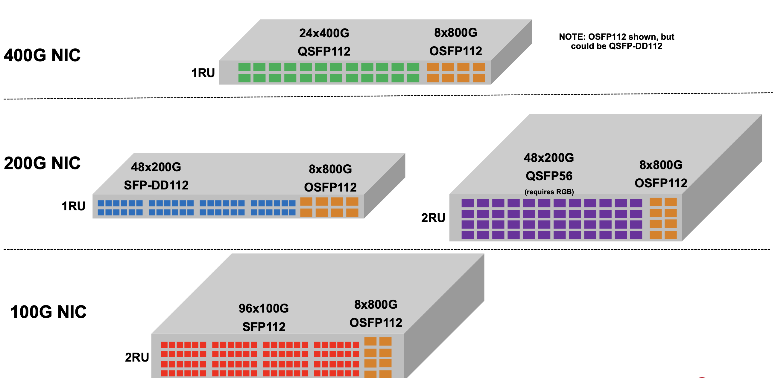
Trident 5 is aimed at top-of-rack switch applications. Typically, 24 or 48 ports of the top-of-rack switch are used for downlinks to connect to servers, while 4 or 8 are used for higher-capacity uplinks (see diagram).
The Trident 5 can support 48 ports of 200 gigabits for the downlinks and eight 800 gigabit for the uplinks. To support 800-gigabit interfaces, the chip uses eight 100-gigabit serdes and an one-chip 800-gigabit media access controller (MAC). Other top-of-rack switch configurations are shown in the diagram.
Currently, 400-gigabit network interface cards are used for demanding applications such as machine learning. Trident5 is also ready to transition to 800-gigabit network interface cards.
Another Tomahawk feature the Trident 5 has adopted is cognitive routing, a collection of congestion management techniques for demanding machine-learning workloads.
One of the techniques is global load balancing. Previous Trident devices supported dynamic load balancing, where the hardware could see the congested port and adapt in real-time. However, such a technique gives no insight into what happens further along the flow path. “If I knew that, downstream, somebody else was congested, then I could make a smarter decision,” says Grindley. Global load balancing does just this. It sends notification to the routing chips upstream that there is congestion so they can all work together.
Another cognitive routing feature is drop congestion notification. Here, packets dropped due to congestion are captured such that what is sent is only their header data and where the packet was dropped. This mechanism improves flow completion times compared to normal packet loss, which is costly for machine-learning workloads.
Trident 5, like its predecessor, Trident 4, has a heterogeneous pipeline of tile types. The tiles contain static random-access memory (SRAM), ternary content-addressable memory (TCAM) or arithmetic logic units. The tiles allow multiple look-ups or actions in parallel at each stage in the pipeline.

Broadcom has a compiler that maps high-level packet-processing functions to its pipeline in the NPL programming language. The latency through the device stays constant, however the packet processing is changed, says Grindley.
Trident 5’s NetGNT inference engine is a new pipeline resource for higher-level traffic patterns. “NexGNT looks at things not at a packet-by-packet level, but across time and the overall packet flow through the network,” says Grindley.
The NetGNT
Until now system architects and network operation centre staff have defined a set of static rules written in software to uncover and treat suspicious packet flows. “A pre-coded set of rules is limited in its ability to catch higher-level traffic patterns,” says Grindley.
When Broadcom started the Trident 5 design, its engineers thought a neural network approach could be used. “We knew it would be useful if you had something that looked at a higher level, and we knew neural networks could do this kind of task,” says Grindley.
The neural network sits alongside the existing traffic analysis logic. Information such as packet headers, or data already monitored and generated by the pipeline, can be fed to the neural network to assess the traffic patterns.
“It sits there and looks for high-level patterns such as the start of a denial of service attack” says Grindley.
Training
The neural network is trained using supervised learning. A human expert must create the required training data and train the model using supervised learning. The result is a set of weights loaded onto the Trident 5’s neural network.

When the neural network is triggered, i.e. when it identifies a pattern of interest, the Trident 5 must decide what it should do. The chip can drop the packets or change the quality of service (QoS). The device can also drop a packet while creating a mirror packet containing headers and metadata. This can then be sent to a central analyser at the network operations centre to perform higher-level management algorithms.
Performance
The Trident 5 chip is now sampling. Broadcom says there is no performance data as end customers are still to train and run live traffic through the Trident 5’s inference engine.
“What it can do for them depends on getting good data and then running the training,” says Grindley. “Nobody has done this yet.”
Will the inference engine be used in other Broadcom networking chips?
“It depends on the market,” says Grindley. “We can replicate it, just like taking IP from the Tomahawk where appropriate.”

ECOC 2023 industry reflections - Final Part
Gazettabyte has been asking industry figures to reflect on the recent ECOC show in Glasgow. The final instalment emphasises coherent technology with contributions from Adtran, Cignal AI, Infinera, Ciena, and Acacia.
Jörg-Peter Elbers, head of advanced technology at Adtran
The ECOC 2023 conference and show was a great event. The exhibition floor was busy and offered ample networking opportunities. In turn, the conference and the Market Focus sessions provided information on the latest technologies, products, and developments.
One hot topic was coherent 800ZR modems. Several vendors demonstrated coherent 800ZR modules and related components. Importantly, these modules also boast new and improved 400 gigabit-per-second (Gbps) modes. The 120 gigabaud (GBd) symbol rate enables 400-gigabit dual-polarisation quadrature phase shift keying (DP-QPSK) transmission over demanding links and long-haul routes. In turn, the advent of 5nm CMOS digital signal processor (DSP) technology enables lower power DP-16QAM than 400ZR modules.
There is broad agreement that the next step in coherent transmission is a 240GBd symbol rate, paving the way to single-wavelength 1.6 terabit-per-second (Tbps) optical transport.
Meanwhile, the use of coherent optical technology closer to the network edge continues. Several players announced plans to follow Adtran and Coherent and jump on the low-power 100 gigabit-per-second ZR (100ZR) ‘coherent lite’ bandwagon. Whether passive optical networking (PON) systems will adopt coherent technology after 50G-PON sparked lively debate but no definitive conclusions.
The OIF 400ZR+ demonstration showed interoperability between a dozen optical module vendors over metro-regional distances. It also highlighted the crucial role of an intelligent optical line system such as Adtran’s FSP3000 OLS in automating operation and optimising transmission performance.
The post-deadline papers detailed fibre capacity records by combining multiple spectral bands and multiple fibre cores. The line-system discussions on the show floor focused on the practical implications of supporting C-, L-, extended, and combined band solutions for customers and markets.
From workshops to the regular sessions, the application of artificial intelligence (AI) was another prominent theme, with network automation a focus area. Examples show not only how discriminative AI can detect anomalies or analyse failures but also how generative AI can improve the interpretation of textual information and simplify human-machine and intent interfaces. For network engineers, ‘Copilot’-like AI assistance is close.
After ECOC is also before ECOC, so please mark in your calendars September 22-26, 2024. ECOC will celebrate its 50th anniversary next year and will take place in Frankfurt, Germany. As one of the General Chairs of the ECOC 2024 event, and on behalf of the entire organising committee, I look forward to welcoming you!
Andrew Schmitt, founder and directing analyst, Cignal AI
ECOC is a great show, it’s like OFC (the annual optical communications and networking event held in the US) but refined to only the critical elements. Here are my key takeaways.
The most impressive demonstration was 800ZR test boards and modules from Marvell and its partners Coherent and Lumentum. Within eight weeks of the first silicon, Marvell has demos up and running in-house and at its partners. The company has at least a 6-month lead in the 800ZR market, making intelligent tradeoffs to achieve this.
Lumentum showed an 8-QAM mode of operation that allows 800 gigabit transmission within a 100GHz channel spacing, which should be interesting. After the massive success of 400ZR, it’s natural to extrapolate the same success for 800ZR, but the use cases for this technology are substantially different. We also heard updates and broader support for 100ZR.
Linear drive pluggable optics (LPO) was a hot topic, although it was our impression that, while optimism ruled public discussion, scepticism was widely expressed in private. There was more agreement than disagreement with our recent report (see the Active Insight: The Linear Drive Market Opportunity). No one is more confident about LPO than the companies who view this as another opportunity to bid for business at hyperscale operators they don’t currently have.
The 200 gigabit per lane silicon/ physical media device (PMD)/ optics development continues, and it is on track to enable 1.6-terabit optics by 2024. Marvell had a more advanced and mature demo of what they showed behind closed doors at OFC. The advancements here are the real threat to adopting LPO, and people need to realise that LPO is competing with the power specs of 200 gigabits per lane, not 100 gigabits per lane solutions.
Also impressive was the comprehensive engineering effort by Eoptolink to show products that covered 100 gigabit and 200 gigabit per lane solutions, both retimed and linear. The company’s actions show that if you have the engineering resources and capital, rather than pick the winning technology, do everything and let the market decide. Also impressive is the CEO, who understood the demos and the seasoned application engineers. Kudos to keeping engaged with the products!
System vendors had a more significant presence at the show, particularly Ciena and Infinera. It’s unsurprising to see more system vendors since they are increasing investments in pluggables, particularly coherent pluggables.
We had many discussions about our forecasts for IPoDWDM deployment growth. This disruption is something that component vendors are excited about, and hardware OEMs view it as an opportunity to adjust how they deliver value to operators (see the Active Insight: Assessing the Impact of IP-over DWDM).
Lastly, the OIF coordinated 400ZR+ and OpenROADM interoperability testing despite the organisation not being directly involved in those industry agreements. The OIF is a fantastic organisation that gets valuable things done that its members need.
Paul Momtahan, director, solutions marketing, Infinera
ECOC 2023 provided an excellent opportunity to catch the latest trends regarding transponder innovation, coherent pluggables and optical line systems. A bonus was getting to the show without needing a passport.
Transponder innovation topics included coherent digital signal processor (DSP) evolution, novel modulators, and the maximum possible baud rate. DSP sessions included the possibility of offloading DSP functions into the photonic domain to reduce power consumption and latency.
There were also multiple presentations on constellation shaping, including enhanced nonlinear performance, reduced power consumption for probabilistic constellation shaping, and potential uses for geometric shaping.
Novel modulators with very high baud rates, including thin-film lithium niobate, barium titanate, plasmonic, and silicon-organic hybrid, were covered. The need for such modulators is the limited bandwidth potential of silicon photonics modulators, though each face challenges such as integration with silicon photonics and manufacturability.
From the baud rate session, the consensus was that 400GBd symbol rates are probable, up to 500GBd might be possible, but higher rates are unlikely. The critical challenges are the radio frequency (RF) interconnects and the digital-to-analogue and analogue-to-digital converters. However, several presenters wondered whether a multi-wavelength transponder might be more sensible for symbol rates above 200 to 250GBd.
Coherent pluggables were another topic, especially at 800 gigabit. However, one controversial topic was the longevity of coherent pluggables in routers (IPoDWDM). Several presenters argued the current period would pass once router port speeds and coherent port speeds no longer align.
As the coherent optical engines approach the Shannon limit, innovation is shifting towards optical line systems and fibres as alternative way to scale capacity.
Several presentations covered ROADM evolution to 64 degrees and even 128 degrees. A contrasting view is that ROADMs’ days are numbered to be replaced by fibre switches and full spectrum transponders, at least in core networks.
Additional options for scaling capacity included increasing the spectrum of existing bands with super-C and super-L. Lighting different bands, such as the S-band (in addition to C+L bands), is seen as the best candidate, with commercial solutions three to five years away.
Overall, it was a great event, and I look forward to seeing how things evolve by the time of next year’s ECOC show in Frankfurt. (For more, click here)
Helen Xenos, senior director, portfolio marketing, Ciena
This was my third year attending ECOC, and the show never disappoints. I always leave this event excited and energised about what we’ve accomplished as an industry.
Every year seems to bring new applications and considerations for coherent optical technology. This year, ECOC showcased the ever-growing multi-vendor ecosystem for 400-gigabit coherent pluggable transceivers, considerations in the evolution to 800-gigabit pluggables, evolution to coherent PON, quantum-secure coherent networking, and the evolution to 200 gigabaud and beyond. When will coherent technology make it into the data centre? A question still open for debate.
Ciena’s optical engineer wizards were on hand to share specifics about our recently announced 3nm CMOS-based WaveLogic 6 technology, which includes the industry’s first performance-optimised 1.6 teraburs-per-second (Tbps) optics as well as 800-gigabit pluggables.
It was exciting for me to introduce customers, suppliers and research graduates to their first view of 3nm chip performance results and show how these enable the next generation of products. And, of course, Ciena was thrilled that WaveLogic 6 was awarded the Most Innovative Coherent Module Product at the event.
Tom Williams, director of technical marketing at Acacia
From my perspective, while there weren’t as many major product announcements as OFC, several trends and technologies continued to progress, including OIF interoperability, 800ZR/ZR+, linear pluggable optics (LPO) and terabit optics.
The OIF interop demonstration was once again a highlight of the show. The booth was at the entrance to the exhibition and seemed to be packed with people each time I passed by.
OIF has expanded the scope of these demonstrations with each show, and this year was the largest ever. In addition to having the participation of 12 module vendors (with 34 modules), the focus was on the ZR+ operation. What was successfully demonstrated was a single-span 400ZR network and a multi-span network.
As co-chair of the OpenZR+ MSA, I was excited by the great collaboration with OIF. These efforts help to drive the industry forward. Karl Gass is not only the most creatively dressed person at every trade show; he is exceptional at coordinating these activities.
It is clear that linear drive pluggable optics (LPO) works in some situations, but views differ about how widespread its adoption will be and how standardisation should be addressed. I lived through the analogue coherent optics (ACO) experience. ACO was essentially a linear interface for a coherent module where the digital processing happened outside the module. For ACO, it was a DSP on the host board and for LPO it is the switch ASIC. The parameters that need to be specified are similar. There is a precedent for this kind of effort. Hopefully, lessons learned there will be helpful for those driving LPO. I am interested to see how this discussion progresses in the industry as some of the challenges are discussed, such as its current limited interoperability and support for 200 gigabits per lane.
There have been announcements from several companies about performance-optimised coherent optics in what we call Class 3 (symbol rates around 140 gigabaud), which support up to 1.2 terabits on a wavelength. Our CIM 8 module has been used in multiple field trials, demonstrating the performance benefits of these solutions.
Our CIM 8 (Coherent Interconnect Module 8) achieves this performance in a pluggable form factor. The CIM 8 uses the same 3D siliconisation technology we introduced for our 400-gigabit pluggables and enables operators to scale their network capacity in a cost- and power-efficient way.

Webinar: Scaling AI clusters with optical interconnects
A reminder that this Thursday, September 14th, 8:00-9:00 am PT, I will be taking part in a webcast as part of the OCP Educational Webinar Programme that explores the future of AI computing with optical interconnects.

Data and computation drive AI success, and the hyperscaler are racing to build massive AI accelerator-based compute clusters. The impact of large language models and ChatGPT has turbocharged this race. Scaling demands innovation in accelerator chips, node linkages, fabrics, and topology.
For this webinar, industry experts will discuss the challenge of scaling AI clusters. The other speakers include Cliff Grossner Ph.D., Yang Chen, and Bob Shine. To register, please click here

Modelling the Human Brain with specialised CPUs

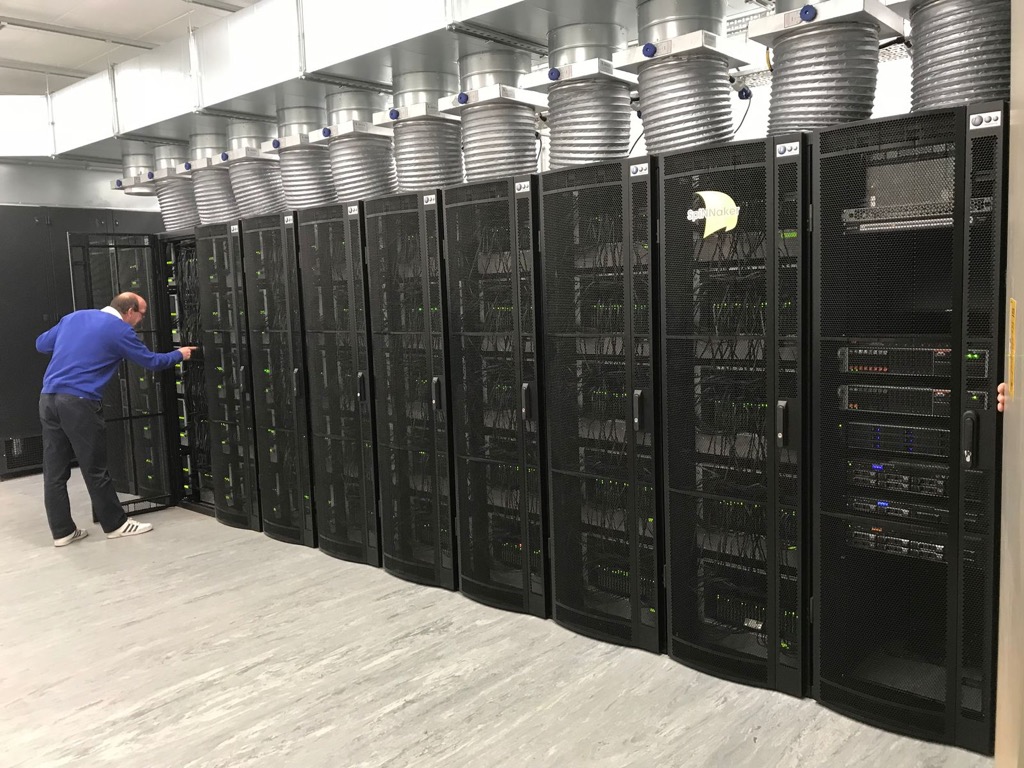
Part 2: University of Manchester’s Professor Steve Furber discusses the design considerations for developing hardware to mimic the workings of the human brain.
The designed hardware, the Arm-based Spiking Neural Network Architecture (SpiNNAker) chip, is being used to understand the working of the brain and for industrial applications to implement artificial intelligence (AI)
Steve Furber has spent his career researching computing systems but his interests have taken him on a path different to the mainstream.
As principal designer at Acorn Computers, he developed a reduced instruction set computing (RISC) processor architecture when microprocessors used a complex instruction set.
The RISC design became the foundational architecture for the processor design company Arm.
As an academic, Furber explored asynchronous logic when the digital logic of commercial chips was all clock-driven.
He then took a turn towards AI during a period when AI research was in the doldrums.
Furber had experienced the rapid progress in microprocessor architectures, yet they could not do things that humans found easy. He became fascinated with the fundamental differences between computer systems and biological brains.
The result was a shift to neuromorphic computing – developing hardware inspired by neurons and synapses found in biological brains.
The neural network work led to the Arm-based SpiNNaker and the University of Manchester’s massively parallel computer that uses one million.
Now, a second-generation SpiNNaker exists, a collaboration between the University of Manchester and University of Technology Dresden. But it is Germany, rather than the UK, exploiting the technology for its industry.
Associative memory
Furber’s interest in neural networks started with his research work on inexact associative memory.
Traditional memory returns a stored value when the address of a specific location in memory is presented to the chip. In contrast, associative memory – also known as content addressable memory – searches all of its store, returning data only when there is an exact match. Associative memory is used for on-chip memory stores for high-speed processors, for example.
Each entry in the associative memory effectively maps to a point in a higher dimensional space, explains Furber: “If you’re on that point, you get an output, and if you’re not on that point, you don’t.”
The idea of inexact associative memory is to soften it by increasing the radius at the output from a point to a space.
“If you have many of these points in space that you are sensitive to, then what you want to do is effectively increase the space that gives you an output without overlapping too much,” says Furber. “This is exactly what a neural network looks for.”
Biological neural networks
Neurons and synapses are the building blocks making up a biological neural network. A neuron sends electrical signals to a network of such cells, while the synapse acts as a gateway enabling one neuron to talk to another.
When Furber looked at biological neural networks to model them in hardware, he realized the neural networks models kept changing as the understanding into their workings deepened.
So after investigating hardware designs to model biological neural networks, he decided to make the engines software programmable. Twenty years on, the decision proved correct, says Furber, allowing the adaptation of the models run on the hardware.
Furber and his team chose the Arm architecture to base their programmable design, resulting in the SpiNNaker chip.
SpiNNaker was designed with massive scale in mind, and one million SpiNNakers make up the massively parallel computer that models human brain functions and runs machine learning algorithms.
Neurons, synapses and networking
Neural networks had a low profile 20 years ago. It was around 2005 when academic Geoffrey Hinton had a breakthrough that enabled deep learning to take off. Hinton joined Google in 2013 and recently resigned from the company to allow him to express his concerns about AI.
Furber’s neural network work took time; funding for the SpiNNaker design began in 2005, seven years after the inexact associative memory began.
Furber started by looking at how to model neural networks in hardware more efficiently: neurons and synapses.
“The synapse is a complex function which, my biological colleagues tell me, has 1,500 proteins; the presence or absence of each affects how it behaves,” says Furber. “So you have very high dimensional space around one synapse in reality.”
Furber and his team tackled such issues as how to encode the relevant equations in hardware and how the chips were to be connected, given the connectivity topology of the human brain is enormous.
A brain neuron typically connects to 10,000 others. Specific cells in the cerebellum, a part of the human brain that controls movement and balance, have up to 250,000 inputs.
“How do they make a sensible judgment, and what’s happening on these quarter of a million impulses is a mystery,” says Furber.
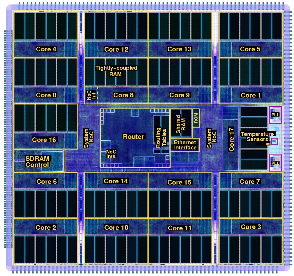
SpiNNaker design
Neurons communicate by sending electrical spikes, asynchronous events that encapsulate information in the firing patterns, so the SpiNNaker would have to model such spiking neurons.
In the human brain, enormous resources are dedicated to communication; 100 billion (1011) neurons are linked by one quadrillion (1015) connections.
For the chip design, the design considerations included how the inputs and outputs would get into and out of the chip and how the signals would be routed in a multi-chip architecture.
Moreover, each chip would have to be general purpose and scalable so that the computer architecture could implement large brain functions.
Replicating the vast number of brain connections electronically is impractical, so Furber and his team exploited the fact that electronic communication is far faster than the biological equivalent.
This is the basis of SpiNNaker: electrical spikes are encapsulated as packets and whizzed across links. The spikes reach where they need to be in less than a millisecond to match biological timescales.
The neurons and synapses are described using mathematical functions solved on the Arm-based processor using fixed-point arithmetic.
SpiNNaker took five years to design. This sounds a long time, especially when the Arm1 took 18 months, until Furber explains the fundamental differences between the two projects.
“Moore’s Law has delivered transistors in exponentially growing abundance,” he says. “The Arm1 had 25,000 transistors, whereas the SpiNNaker has 100 million.”
Also, firms have tens or even 100s of engineers designing chips; the University of Manchester’s SpiNNaker team numbered five staff.
One critical design decision that had to be made was whether a multi-project wafer run was needed to check SpiNNaker’s workings before committing to production.
“We decided to go for the full chip, and we got away with it,” says Furber. Cutting out the multi-project wafer stage saved 12% of the total system build cost.
The first SpiNNaker chips arrived in 2010. First test boards had four SpiNNaker chips and were used for software development. Then the full 48-chip boards were made, each connecting to six neighbouring ones.

The first milestone was in 2016 when a half-million processor machine was launched and made available for the European Union’s Human Brain Project. The Human Brain Project came about as an amalgam of two separate projects; modelling of the human brain and neuromorphic computing.
This was followed in 2018 by the entire one million SpiNNaker architecture.
“The size of the machine was not the major constraint at the time,” says Furber. “No users were troubled by the fact that we only had half a million cores.” The higher priority was improving the quality and reach of the software.
Programming the computer
The Python programming language is used to program the SpiNNaker parallel processor machine, coupled with the Python Neural Network application programming interface (PyNN API).
PyNN allows neuroscientists to describe their networks as neurons with inputs and outputs (populations) and how their outputs act as inputs to the next layer of neurons (projections).
Using this approach, neural networks can be described concisely, even if it is a low-level way to describe them. “You’re not describing the function; you’re describing the physical instantiation of something,” says Furber.
Simulators are available that run on laptops to allow model development. Once complete, the model can be run on the BrainScaleS machine for speed or the SpiNNaker architecture if scale is required.
BrainScaleS, also part of the Human Brain Project, is a machine based in Heidelberg, Germany, that implements models of neurons and synapses at 1000x biological speeds.
Modeling the brain
The SpiNNaker computer became the first to run a model of the segment of a mammalian cortex in real biological time. The model of the cortex was developed by Jülich Research Centre in Germany.
“The cortex is a very important part of the brain and is where most of the higher-level functions are thought to reside,” says Furber.
When the model runs, it reproduces realistic biological spiking in the neural network layers. The problem, says Furber, is that the cortex is poorly understood.
Neuroscientists have a good grasp of the Cortex’s physiology – the locations of the neurons and their connections, although not their strengths – and this know-how is encapsulated in the PyNN model.
But neuroscientists don’t know how the inputs are coded or what the outputs mean. Furber describes the Cortex as a black box with inputs and outputs that are not understood.
“What we are doing is building a model of the black box and asking if the model is realistic in the sense that it reproduces something we can sensibly measure,” says Furber
For neuroscientists to progress, the building blocks must be combined to form whole brain models to understand how to test them.
At present, the level of testing is to turn them on and see if they produce realistic spike patterns, says Furber.
SpiNNaker 2
A second-generation SpiNNaker 2 device has been developed, with the first silicon available in late 2022 while the first large SpiNNaker 2 boards are becoming available.
The original SpiNNaker was implemented using a 130nm CMOS process, while SpiNNaker 2 is implemented using a 22nm fully depleted silicon on insulator (FDSOI) process.
SpiNNaker 2 improves processing performance by 50x such that a SpiNNaker 2 chip exceeds the processing power of the 48- SpiNNaker printed circuit board.
SpiNNaker 2’s design is also more general purpose. A multiply-accumulator engine has been added for deep learning AI. The newer processor also has 152 processor engines compared to Spinnaker’s 18, and the device includes dynamic power management.
“Each of the 152 processor engines effectively has its dynamic voltage and frequency scaling control,” says Furber. “You can adjust the voltage and frequency and, therefore, the efficiency for each time step, even at the 0.1-millisecond level; you look at the incoming workload and just adjust.”
The University of Technology Dresden has been awarded an $8.8 billion grant to build a massively parallel processor using 10 million SpiNNaker 2 devices.
The university is also working with German automotive firms to develop edge-cloud applications using SpiNNaker 2 to process sensor data with milliseconds latency.
The device is also ideal for streaming AI applications where radar, video or audio data can be condensed close to where it is generated before being sent for further processing in the cloud.
Furber first met with the University of Technology Dresden’s neuromorphic team via the Human Brain Project.
The teams decided to collaborate, given Dresden’s expertise in industrial chip design complementing Furber and his team’s system expertise.
Takeaways
“We are not there yet, says Furber, summarizing the brain work in general.
Many practical lessons have been learnt from the team’s research work in developing programmable hardware at a massive scale. The machine runs brain models in real time, demonstrating realistic brain behaviour.
“We’ve built a capability,” he says. “People are using this in different ways: exploring ideas and exploring new learning rules.
In parallel, there has also been an explosion in industrial AI, and a consensus is emerging that neuromorphic computing and mainstream AI will eventually converge, says Furber.
“Mainstream AI has made these huge advances but at huge cost,” says Furber. Training one of these leading neural networks takes several weeks consuming vast amounts of power. “Can Neuromorphics change that?”
Mainstream AI is well established and supported with compelling tools, unlike the tools for neuromorphic models.
Furber says the SpiNNaker technology is proven and reliable. The Manchester machine is offered as a cloud service and remained running during the pandemic when no one could enter the university.
But Furber admits it has not delivered any radical new brain science insights.
“We’ve generated the capability that has that potential, but no results have been delivered in this area yet, which is a bit disappointing for me,” he says.
Will devices like SpiNNaker impact mainstream AI?
“It’s still an open question,” says Furber. “It has the potential to run some of these big AI applications with much lower power.”
Given such hardware is spike-driven, it only processes when spiking takes place, saving energy. As does the nature of the processing, which is sparse, areas of the chip tend to be inactive during spiking.
Professor Emeritus
Furber is approaching retirement. I ask if he wants to continue working as a Professor Emeritus. “I hope so,” he says. “I will probably carry on at that moment.”
He also has some unfinished business with model aircraft. “I’ve never lost my itch to play with model aeroplanes, maybe I’ll have time for that,” he says.
The last time he flew planes was when he was working at Acorn. “Quite often, the aeroplanes came back in one piece,” he quips.
For Part 1: From 8-bit micros to the modeling the human brain, click here
Further information
Podcast: SpiNNaker 2: Building a Brain with 10 Million CPUs