
Evolving packet processing by a factor of 1000
Nokia’s FP5 IP router chipset has been a design four years in the making, the latest iteration of a two-decades-old packet processing architecture.
The 3-device FP5 chipset is implemented using a 7nm CMOS process. The design uses 2.5D stacked memory and is the first packet processor with 112 gigabit-per-second (Gbps) serialiser-deserialiser (serdes) interfaces. Also included are line-rate hardware encryption engines on the device’s ports.

Ken Kutzler
What hasn’t been revealed are such metrics as the chipset's power consumption, dimensions and transistor count.
Ken Kutzler, vice president of IP routing hardware at Nokia IP Networks Division, says comparing transistor counts of chips is like comparing software code: one programmer may write 10,000 lines while another may write 100 lines yet both may execute the same algorithm.
“It’s not always the biggest and baddest chip in the world that compares well,” says Kutzler.
GPU-CPU union
Kutzler says the FP5 can be characterised as combining the attributes of a graphics processing unit (GPU) with a general-purpose processor (CPU).
A GPU must deal with massive amounts of data - pixels - flowing through the device. “It’s a data flow model and that is what a packet processor has to do,” he says. A CPU, in contrast, processes data in blocks. A lot of the data processing involves moving data.
“You don't want to spend all that time with the processor moving data around, you want the data to move and the processing acting upon it,” says Kutzler. This is what the FP5 does: processes data as it flows.
“Our device has to be like a GPU in how data moves and like a CPU in that it has to be general-purpose,” he says. By general purpose, Nokia means having a programmable packet-processing pipeline rather than predefined hardware accelerator blocks.
“For service providers, the amount of features are pretty intense and they are ever-changing,” says Kutzler. “We have tended to forgo specialised engines that presuppose how something is parsed.”

Source: Nokia, Gazettabyte
Programmable pipelines
As implied by the name, the FP5 is the fifth-generation implementation of what started in 2003 as Alcatel’s FP packet processor. The FP had a 10Gbps line rate and used 30 packet-processing cores that ran microcode, each core being clocked at 190MHz.
The Alcatel-Lucent FP2 followed in 2007. The 100Gbps FP2 nearly quadrupled both the cores (112) and their clock rate (840MHz) and the trend continued with the 400Gbps FP3 announced in 2011.
The FP3 has 288, 1GHz cores arranged in a 2D array: 32 rows by 9 columns. Each row acts as a packet-processing pipeline that can be partitioned to perform independent tasks. The columns perform table look-ups and each column can be assigned more than one task.
The FP3 continues to carry IP network traffic and have its features enhanced using software upgrades, highlighting the benefit of a programmable packet processing architecture, says Kutzler.
The chipsets are also backwards compatible; the FP5 can implement the FP3’s instruction set, for example, but it also includes newer instructions. In one clock cycle, multiple instructions can be executed in an FP5 core. The core also supports multi-threading that did not exist with the FP3 whereby several instruction threads are interleaved and processed in parallel.
Chipset partitioning
Kutzler stresses that Nokia sells platforms and solutions, not chips. What matters to Nokia is that the silicon meets its platform requirements.
“I don’t really care what the ASIC speed is because I’m not going to sell it,” says Kutzler. “I care what the board speeds want.” For FP5-enabled platforms, that is 14.4 terabits.
But some customers want 2.4-terabit and 4.8-terabit capacities so what is needed is a power-efficient cost-effective solution across designs.
Partitioning the chipset functionality is reconsidered with each generation of design. “We will move things where it makes the most sense when designing our entire solution,” says Kutzler.
The 16nm CMOS 3Tbps FP4 chipset comprises a packet processor (p-chip) and the traffic manager (q-chip) as well as what was then a new chip, the e-chip. A media access controller (MAC), the e-chip parcels data from the router’s client-side pluggable optical modules for the packet processor.
However, Nokia combined the s-chip and t-chip withe FP4; the s-chip is a switch IC while the t-chip interfaces to the router’s fabric.
With the 7nm CMOS FP5, the p-chip and q-chip have finally been combined along with the t-chip.
Kutzler says the p- and q-chips could have been combined with earlier generation designs. But given the die cost (yield), it was deemed better to keep them separate. This also has system advantages: some FP3-based systems were configured using a combination of two p-chips and one q-chip.
“The p-chip is malleable; you can put it serially or in parallel,” says Kutzler. The compiler is told how the design is set up and the microcode is compiled accordingly.
The latest partitioning means the FP5 is a three-device chipset: the main chip (the packet processor, traffic manager and fabric interface), s-chip and the e-chip.
Terabit scale
The FP4 required a significant redesign for the architecture to continue to scale that took six years rather than its typical four-year design cycle.
“These were low-level changes, it [the FP4] still runs the same microcode but enhanced in such a way that the architecture can evolve,” says Kutzler.
The FP4 uses 1,040 cores, each enhanced to execute two instructions per clock cycle. The die-shrink allowed the cores to be clocked at 1.5GHz and hyper-threading was added, as mentioned. The FP4 also adopted 56Gbps serdes technology from Broadcom.
“When we talked about the FP4, we said it is setting this up for FP5 and that the FP5 would be coming much faster,” says Kutzler.
The FP5 increases the core count to 1,248 and doubles the serdes speed to 112Gbps.
“Serdes consume a considerable amount of power,” says Kutzler. Yet doubling the serdes speed saves power overall; a 112Gbps serdes consumes more power than a 56Gbps one but much less than twice the power.
Equally, putting two devices (the p-chip and q-chip) into one chip saves power otherwise required for chip-to-chip communications. Power is also saved when certain device features are not in use.
Nokia claims the FP5 design consumes a quarter of the power of the FP4 ones when measured in Watts-per-gigabit (0.1W/gigabit compared to 0.4W/gigabit).
The 0.1W/gigabit is with the chipset’s features turned on including the encryption engines. “If a limited feature set is required, our expected power numbers will be below the full-featured typical power consumption number,” says Jeff Jakab, Nokia’s director of IP routing hardware.
Memory
One issue IP router chip designers face is that the line rates of their chips are rising far faster than memory access speeds.
There are two memory types used for routing, each with its own requirements, says Nokia.
The first memory type is used for counters and table look-ups while the second buffers packets.
For counters/ look-ups what is needed is very high-speed memory that supports 32-bit and 64-bit reads and writes. In contrast, buffering requires much larger memories; the packet blocks are much larger requiring bigger reads and writes but they are not as simultaneous, says Kutzler.
Nokia developed its own ‘smart memory’ for the FP4 that is command-line driven. This means that a command can be used to perform a task that otherwise would require multiple memory accesses, thereby adding much-needed parallelism.
Four such smart memory dies are included in the FP4’s p-chip while for buffering, four high-bandwidth memory (HBM) blocks, each comprising stacked memory die, are part of the q-chip.
The FP5 integrates the smart memory on-chip, freeing up room for the latest HBM2e technology. “This allows us to get the speeds we need,” says Kutzler. “So when we say we have a 14.4-terabit card, it allows true QoS (quality of service) on every packet.”
“All chipsets released prior to the FP5 make use of HBM2 and are constrained to a maximum of some 1.7 terabits of full-duplex bandwidth to buffer memory,” says Jakab.
The FP4's HBM2 buffer memory supports a 1.5-terabit line rate whereas HBM2e can support a 2.4-terabit line rate.
“We are not aware of any other chipsets on the market that make use of HBM2e,” says Jakab, adding that these memory types generally cannot be substituted one for another without considerable redesign effort.
Nokia’s use of memory includes the FP5’s e-chip which plays a key role, as is now explained.
Board considerations
The e-chip is deliberately separated from the main chip as it performs packet pre-processing and packet pre-classification as well as pre-buffering in front of the packet processor.
“We use multiple e-chips in front of our packet processor to allow the faceplate of our card to expand in terms of port capabilities beyond the forwarding limit of our packet processor,” says Jakab.

Jeff Jakab
The e-chip delivers two advantages. It does away with pre-aggregation boxes in front of Nokia’s 7750 SR platform. Such 1 rack unit (1RU) pre-aggregation boxes are used to groom traffic into an edge router or smart aggregation platform.
A typical pre-aggregation box supports 32MB of buffering, says Jakab, whereas each e-chip uses nearly 20x that amount.
“It [using the e-chip] collapses the platforms in front, saving power and rack space while eliminating a layer from the network,” says Jakab.
In many IP edge or core applications, customers are not capacity restricted but port restricted. They run out of ports long before they run out of capacity because the majority of flows are all fractional.
A fractional flow is one that does not fill up the full bandwidth of an interface, for example 50 gigabits of traffic on a 100-gigabit interface or 7 gigabits of traffic on a 10 Gigabit Eternet interface.
This is the design use case of Nokia’s SR-1 router platform. “Aggregating a ton of fractional flows with many many connectivity option types is the ideal use case for smart aggregation," says Jakab.
The e-chip also helps Nokia's systems to benefit from what it calls intelligent aggregation which uses pre-classification and pre-buffering to guarantee the flows that matter most.
“It goes well beyond basic oversubscription because we pre-buffer and pre-classify to ensure that high priority traffic is always guaranteed,” says Jakab.
This is different from classic oversubscription where, when the given rate for a packet processor is exceeded, the next packet is by default discarded, irrespective of QoS, says Jakab.
“It means we can flexibly offer more ports on the faceplate of a card to satisfy increasing port requirements without fear of indiscriminate packet drops,” he says.
Nokia points out that its FP5 line cards expand capacity by 3x.
Its 4.8Tbps expandable media adaptor (XMA) card supports 12 terabit of intelligent aggregation by using four FP4 chipsets. Its latest XMA is 14.4Tbps, supports 19.2Tbps of IA, and uses six FP5 chipsets.
What next
Extrapolating four years hence to 2025, the FP6 packet processor will likely be a 5nm or 3nm CMOS design with a packet-processing capacity of some 10Tbps, a 1000x improvement on the first FP.
Kutzler stresses that the speed of the device is less important than meeting its IP system requirements for the decade that will follow. It is these requirements that will shape the FP6 design.
Kutzler did share one thing about the FP6: it will use 224Gbps serdes.

Ciena builds its IP edge
-
The background to Ciena's Vyatta acquisition
Ciena’s acquisition of AT&T’s Vyatta team is a further step in its campaign to bolster its internet protocol (IP) expertise.
Ciena will gain 60 IP engineers with expertise in network operating systems (NOS).

Joe Marsella
“If you believe that IP-optical convergence is a trend, and Ciena does, then you need expertise in both areas,” says Joe Marsella, vice president, product line management, routing and switching at Ciena.
Ciena has been growing its IP expertise for the last five years. “We are competing against companies that have been doing this for 30 years,” says Marsella. “The more experience we can bring in, the more it helps us.”
Ciena says the deal emerged gradually. ”I can’t say it was a Ciena or an AT&T idea; it was a mutual discussion over time that finally resulted in an acquisition,” says Marsella.
Ciena will also gain its first R&D centre in Europe. The deal is expected to be completed before the year-end.
Vyatta
Vyatta, a privately-held company founded in 2005, was acquired a decade ago by Brocade to help the company address virtualisation, public cloud, enterprise, and managed services.
Communications service provider (CSP) AT&T then bought Vyatta’s NOS and certain Brocade assets in 2017 as part of its strategy to virtualise its network. The Vyatta team also enhanced AT&T’s SD-WAN and white box capabilities.
The Vyatta team was an integral part of AT&T’s dNOS software framework developed for open routing that was contributed to the Linux Foundation as the Disaggregated Network Operating System (DANOS) project.
Now Ciena is acquiring the unit as AT&T divests elements of its in-house expertise.
“Many of the Vyatta folks were at Brocade, AT&T and now at Ciena,” says Marsella. “This is a pretty consistent team and that experience is super helpful for us.”
Applications
Ciena’s virtualised edge solution is based on a platform onto which third-party virtual network functions (VNFs) are executed. Such VNFs include SD-WAN, firewalls, virtual routing, and encryption.
The platform uses Ciena’s distributed NFV infrastructure (D-NFVI) software that runs on its server platforms or commercial-off-the-shelf (COTS) servers. Ciena uses its service-aware operating system (SAOS 10.x) as part of the offering.
“That platform that we built is largely about being a neutral host to other people’s virtualisation products,” says Marsella; an approach that suits many customers.
But some customers don’t want to deal with the complexities of mapping VNFs onto the underlying hardware. “They just want a virtual router to work on the virtual platform,” he says.
Adding the Vyatta unit’s IP NOS and deployment know-how will enable Ciena serve both customer sets.
“There are certain verticals, there are certain capabilities that they [Vyatta] have built into their OS that we don’t have today in our SAOS 10.x,” says Marsella.
The new unit also has expertise in disaggregation platforms where software is executed on merchant silicon in a white box.
“Our SAOS 10.x supports disaggregation as well but one of the biggest hurdles as you integrate onto hardware is the data path,” says Marsella. “They have experience in that mapping.”
Ciena’s interest in the virtualised edge covers mobility, enterprise and residential. “Edge is all three and everything in between because there is a lot of overlap between them,” says Marsella.
For mobility, he cites cell-site gateways, while for enterprise the services include SD-WAN and firewalls as well as host platforms such as a micro-CPE and network interface devices (NIDs). Ciena’s residential edge interest, meanwhile, is from its 10-gigabit XGS-PON activities.
Custom versus disaggregated routing
The traditional IP router vendors develop custom silicon such as Cisco’s Silicon One portfolio and Nokia’s FP5 chipset.
A more recent routing development is to use merchant silicon and disaggregated designs, with white box platforms from the likes of Ufispace, Edgecore and Delta based on Broadcom silicon and software such as DriveNets’ Network Cloud.
Ciena says its strategy remains unchanged with the Vyatta acquisition.
“We can run our OS in a disaggregated manner, running SAOS 10.x on a white box, but we also run that same operating system on our hardware platforms,” says Marsella. “But we do build our hardware platforms from merchant silicon; that is the current strategy.”
Using virtualisation, a virtual router running on an Intel processor is suited to applications closer to the edge. “As you move closer to the core, that model doesn’t work as well but it doesn’t mean you can’t run it in a disaggregated [hardware and software] way,” says Marsella. “That is a core router application but it is using disaggregated software but still running on pretty hefty Broadcom-based UfiSpace-built hardware.”
Ciena supports virtualisation and disaggregation models, depending on the network location. “But we haven’t invested in building our own silicon,” says Marsella.
The Blue Planet platform's ongoing automation journey
Vodafone UK is one operator that has recently chosen Ciena's Blue Planet for the management of its optical and IP networks. An interview with Ciena to understand what the Blue Planet network automation tool does.
Having some knowledge of a telco's operations helps in understanding the role of a network automation platform. So says Kevin Wade, senior director and product marketing team leader at Ciena Blue Planet.

Source: Ciena
Service providers, like any business, have an operational infrastructure that begins with business processes. For a service provider, the process starts with a connectivity service request. The business processes capture the customer's order and deliver the requested service.
Once up and running, the service must be monitored and managed to ensure the service level agreement is upheld.
"Today, these processes are highly manual," says Wade. "Automation is being looked at and deployed more extensively to simplify these processes."
Blue Planet's evolution
Blue Planet's capabilities have expanded considerably since Ciena bought the platform from Cyan in 2015. Then, it was an orchestration tool for network functions virtualisation (NFV).
The platform now addresses automated operations or, as the company describes it, closed-loop service-life-cycle automation.
Ciena bought three companies between 2018-19 to bolster the Blue Planet platform.

Kevin Wade
Packet Design, its first acquisition, provides Layer 3 automation. Cyan, like Ciena, was a packet-optical company so Blue Planet addressed up to Layer 2. "Layer 3 is where the real intelligence is in the network," says Wade.
Packet Design's expertise is in route optimisation, understanding the Layer 3 network's real-time topology and determining the best provisioned dynamic paths using multiprotocol label switching (MPLS).
An issue impacting network automation is that operators may be ignorant of all the equipment they have deployed. Given the long deployment histories, operators can lose track of equipment in their networks. "It's like running a store and not knowing what you have in the back room," says Wade.
To this aim, Ciena bought DonRiver which developed a tool that maps the elements making up the network and reveals their relationship to the services. This is now Blue Planet's Inventory product (see diagram).
The tool has a 'federation engine' that collects network data. The engine uncovers relationships between network components and the topology, including items such as patch panels and cables, and relates the services to the topology.
"This [capability] is outside the closed-loop automation process but is critical to help customers accelerate the automation journey," says Wade.
The third and final acquisition, and the most important in expanding Blue Planet's capabilities, is Centina Systems which brings assurance expertise.
"Assurance ensures that a service is provisioned correctly and monitored in real-time using information from across the multi-domain, multi-layer network," says Wade. This capability helps network operations centre staff fix faults.
Collectively, the capabilities help operators understand what is deployed so they can automate, implement automated service activation from Layers 0-3, and assure the automated services in a continuous and closed-loop manner, says Wade.
Modular platform
Ciena is a member of the Linux Foundation Networking's Open Network Automation Platform (ONAP) initiative. ONAP is an open-source project developing an orchestration, management and automation platform for network services.
By joining the open-source initiative, Ciena can pick ONAP components and integrate them with its software. "We support it [a component], enhance it, and integrate it with Blue Planet," says Wade.
Ciena worked on and integrated ONAP's policy engine within Blue Planet which has since been deployed by a service provider customer active in ONAP.
The service provider suggested Ciena's policy-engine enhancements would be valuable to the ONAP open-source community. Ciena worked with the operator to take control of the policy engine before contributing it back to the community. The resulting policy engine is now a component of Blue Planet and ONAP.
"It is interchangeable between the two," says Wade. "That is the concept operators are looking for across all the software components implemented in their stack; they want it modularised."
Ciena is making other modules available to operators aside from the policy engine. These include its Layer-3 path computation engine (PCE) and what it calls its 'discovery layer'.
When Blue Planet automates a service, it drills down to the multi-vendor network management systems or software-defined networking (SDN) controllers. "As a functional block, this is a discovery layer," says Wade. "Customers have requested we make this module available."
Wade says that the larger operators have more developer staff to integrate individual components: "Some operators are interested in buying certain high-value functions inside Blue Planet as standalone components."
Service provider customers
Ciena has over 200 Blue Planet customers including 15 tier-1 service providers.
Vodafone UK, for example, is introducing a transport domain orchestrator and is using Blue Planet as the first step towards end-to-end automation.

Hector Silva
Telefonica Deutschland announced last year that it had chosen Ciena's software for its network upgrade as part of its iFusion programme. This includes SDN and a multi-vendor transport network.
Hector Silva, CTO and strategic sales leader for CALA at Ciena, says Telefonica Deutschland selected Blue Planet for its support of open standard models such as the transport application programming interface (T-API) and OpenConfig.
"Operators have to have everything standardised, supporting the OpenConfig and T-API models; that is a direction they want to go," says Silva. "But Blue Planet also has the flexibility to support legacy interfaces."
The Telefonica architecture uses a hierarchical SDN approach. At the lower level are various vendors' equipment above which reside SDN domain controllers that are typically vendor specific. And above that is the Blue Planet platform.
"Blue Planet communicates to the domain controllers or directly to the equipment," says Silva. "The vision is to have those interfaces and the models standardised."
Blue Planet abstracts that complexity underneath so that the services connected to Ciena's software see a consistent service definition end-to-end. "This is regardless of the mix of vendors and systems," says Silva.
Blue Planet exposes the information to the operations system support (OSS) above it. "This becomes a point of entry for assurance and inventory such that all these resources are consolidated in a single application programming interface (API)," says Silva.
Dish Network is another service provider that is using Blue Planet. In particular, the Blue Planet Inventory tool and the service order management that helps automate the processing of service orders.
Dish is getting ready for 5G network slicing and both tools are helping the operator. "Quickly processing a customer order is part of network slicing; the idea of changing and modifying on-demand," he says.
Colt Technology Services is another operator that has trialled Blue Planet's Proactive Network Operations (PNO) tool. The tool uses machine-learning techniques to predict faults in the network so they can be addressed before the fault occurs.
“Proactive Network Operations helps providers not only predict unplanned outages with extraordinary accuracy – up to 95 per cent – but also avoid them,” says Wade. Using such automation and artificial intelligence capabilities, Proactive Network Operations save providers on average some 38 per cent in ‘trouble-to-resolve’ operational expenses a year.
Wade says Colt is using the tool in an open-loop manner with staff assessing the machine-learning algorithm's recommendations.
Closed-loop control may happen for certain alarms but staff are likely to be involved awhile yet.

400-gigabit coherent modules finally hit their stride
NeoPhotonics discusses 400-gigabit coherent modules, the move to 130-gigabaud symbol-rate optical components and a company tunable laser milestone.
NeoPhotonics’ 400ZR pluggable optical modules are now available and will ship in volume from the autumn.

Ferris Lipscomb
“The QSFP-DD and OSFP 400ZR [optical modules] have passed qualification tests and we are engaged in numerous customer qualifications around the world,” says Ferris Lipscomb, vice president of marketing at NeoPhotonics.
400ZR modules implement the OIF’s 400-gigabit standard to connect directly equipment in data centres up to 120km apart without needing separate dedicated dense wavelength-division multiplexing (DWDM) optical transport equipment. The first 400ZR modules will be used by data centre operators.
But coherent pluggables support longer-reach modes. These may be interoperable if implementing the OpenZR+ multi-source agreement (MSA) or when delivering custom optical performance that are referred to as ZR+ modules.
NeoPhotonics has reported that its 400-gigabit coherent QSFP-DD when operated as a ZR+ module can achieve an 800km reach.
At the OFC 2021 virtual conference and exhibition, NeoPhotonics discussed its multi-rate CFP2-DCO module that has a reach of 1,500km at 400 gigabits. Here, 64 gigabaud (GBd) and 16-ary quadrature amplitude modulation (16-QAM) are used along with probabilistic constellation shaping and a proprietary forward error correction scheme.
Probabilistic shaping manipulates the data before transmission so that the inner four constellation points more frequently carry data than the outer 12. Using this signal processing approach improves the overall distance between the constellation points used.
“Taken together, these two [the ZR+ and the CFP2-DCO] show that pluggable modules will have much broader applications than just data centre interconnect over 80-120km,” says Lipscomb.
NeoPhotonics’ CFP2-DCO module uses indium phosphide-based components while its QSFP-DD ZR/ZR+ module employs a silicon photonics-based coherent optical sub-assembly (COSA).
When Western telcos will adopt the CFP2-DCO pluggable is to be determined, says Lipscomb, but the Chinese operators are already using it. In China, the CFP2-DCO module employs quadrature phase-shift keying (QPSK) modulation instead of 16-QAM to enable distances beyond 1,000km at 200-gigabit wavelengths.
Two-hundred gigabits implemented using 64GBd and QPSK rather than a 32GBd symbol rate and 16-QAM enables more space between the points on the constellation diagram so that there is more resiliency to degradation before the received points blend.
At 400 gigabits, the performance of these modules is approaching that of line cards, says Lipscomb, yet they are much cheaper, have a lower power consumption and are more convenient to use.
NeoPhotonics has also shown 36 of its QSFP-DD coherent modules in an Arista Networks’ switch. “This shows it has low-enough power management capability to fully load an Arista switch,” says Lipscomb.
Adding coherent optics in the form of pluggables to a switch reduces the overall cost to a quarter that of existing architectures where a separate optical networking platform is required as well as extra optical transceivers linking the two.
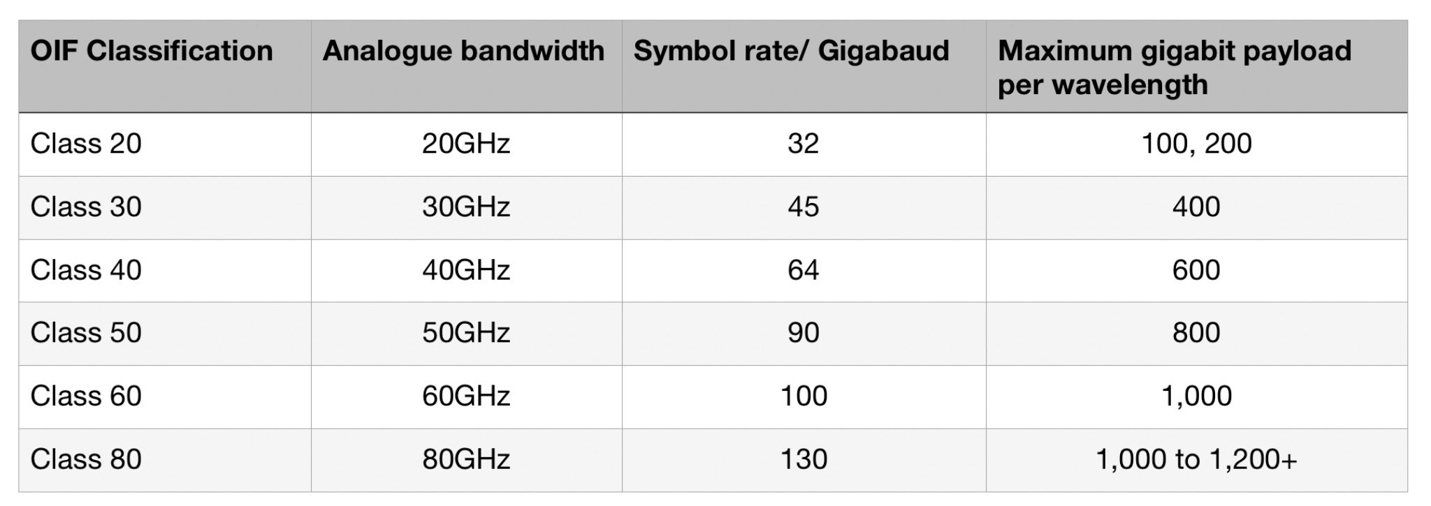
Class 80 components
Tim Jenks, chairman and CEO of NeoPhotonics, has detailed how the company will extend the bandwidth of its indium phosphide coherent integration platform to operate at a symbol rate of 130GBd.
NeoPhotonics is already shipping in limited quantities its Class 60 devices. These are defined as having a three decibel (dB) bandwidth at 60GHz such that they operate at a symbol rate of 96GBd. Such devices enable coherent wavelengths up to 800 gigabit.
In contrast, Class 80 optical components - the driver modulator and the integrated coherent receiver - have a 3dB bandwidth at 80GHz, suitable for 130GBd. Such devices will enable 1 terabit, 1.2-terabit and even greater speed wavelengths. (See Table.)
NeoPhotonics, Gazettabyte
The hare and the tortoise
Class 80 coherent designs will require new optics as well as a next-generation 5nm coherent digital signal processor (DSP).
Such coherent systems will extend the reach and reduce cost but will not improve spectral density. “As you go to higher baud rates, you have to expand the channel width,” says Lipscomb. “So you get fewer channels in the same band.” This is also why cost comes down as fewer modules will be needed overall.
While there is a clear path for the optics to reach 130GBd, says Lipscomb, developing the faster analogue-to-digital and digital-to-analogue converters, the 5nm DSP, and the connectors, is more challenging.
Borrowing from the Aesop fable, Lipscomb equates the optics to the hare and the DSP to the tortoise.
It is not that the optics is so much ahead but that the DSP depends on the availability of the next CMOS process node and that is highly predictable.
“The DSP is the tortoise,” says Lipscomb. “It is going to get there at a certain rate, you can count on it.” The optics might sprint ahead but then it may take longer to scale up production. Overall though, the optics tracks the DSP’s availability.
Lipscomb expects 128GBd systems to be trialled next year with deployments starting in 2023. The individual baud rate used by a system can vary between 120-130GBd but in general 128GBd, as a multiple of 32 and 64GBd rates, is used as a reference symbol rate for Class 80 devices.
Pluggables versus line cards
Lipscomb says the high-end, longest-reach optical networking applications will be served using line cards based on 130GBd coherent systems.
People will pay for the high-end optical performance of such line card-based coherent optics because they will need it, so the segment will continue to be profitable, says Lipscomb.
But the bulk of the [coherent] work will increasingly be served using pluggables, first 400 gigabits at 64GBd and then at 800 gigabits operating at 96GBd.
“They won’t be the most efficient,” he says. “But they will be the cheapest because of the pluggability and will have lower power.”
Coherent sensing and tunable lasers
NeoPhotonics is also applying its coherent know-how for other non-telecom applications such as driverless cars (LiDAR), industrial sensing and medical sensing.
Industrial sensing refers to precise measurement of components while the medical sensing application - optical coherent tomography - allows probing a few millimetres deep under the skin.
“We provide principally lasers but also some other components that are used in coherent-sensing applications,” says Lipscomb.
NeoPhotonics recently shipped its 2 millionths narrow linewidth laser since 2011.
NeoPhotonics acquired Santur and its narrow linewidth laser in 2011 followed by Emcore in 2014. Initially what was used was the integrable tunable laser assembly (ITLA), followed by the more compact micro-ITLA and then the nano-iTLA. Lipscomb says that the size of the original ITLA is comparable to a QSPD-DD coherent module.
“In that timeframe [since 2011], some 3 million coherent ports have been shipped,” says Lipscomb. “Some parts use one laser and some use two; you can do the maths but we have a very significant presence in the majority of the coherent ports that have shipped.”

BT takes a deep dive into hollow-core fibre
BT has been experimenting with hollow-core fibre to understand how it could benefit its network. The results are promising.

Professor Andrew Lord
“We are looking at all the use cases and it is a bit early to say which one is the killer one but they are all interesting,” says Professor Andrew Lord, BT’s head of optical network research.
“There are so many parameters [of hollow-core fibre] and all seem to be slightly or vastly better than single-mode fibre,” says Neil Parkin, optical networks research manager at BT.
The service provider is working with hollow-core fibre start-up, Lumenisity, and 5G software networking specialist, Mavenir.
Hollow-core fibre
Hollow-core fibre is not new. Several firms pursued the technology in the early 2000s but the technology failed to be adopted and the firms folded.
BT Labs is investigating the fibre anew because the optical loss performance of Lumenisity's fibre has improved greatly in recent years.
“Hollow-core fibre might have been interesting for devices but if it carries on [progressing], it looks like it will be useful in the network,” says Lord.
Standard optical fibre uses a solid glass core surrounded by cladding. The core has a higher refractive index than the cladding which confines the light to the core. But being glass, the speed of the light in the core is two-thirds that of the fundamental speed of light.
Hollow-core fibre, in contrast, uses an air-based core. Data sent along the fibre travels at a speed approaching that of the fundamental speed of light, some 50 per cent faster than traditional fibre. In terms of latency, this corresponds to a 30 per cent reduction.
Hollow-core fibre is thus ideal for applications where getting data to the destination as quickly as possible is key.
Companies such as OFS Fitel and Lumenisity, a University of Southampton spin-off, now offer hollow-core fibre commercially.
Hollow-core fibre typically is based on a photonic bandgap design. This results in multi-mode transmission in the core such that the fibre must be designed to filter the higher-order modes. In contrast, Lumenisity uses what it calls a nested, anti-resonant nodule fibre (NANF) design that is inherently single-mode.
"We are probably the first telco to have this hollow-core NANF design," says Parkin.
Optical performance merits
The flagship optical performance benefit of hollow-core fibre is its low latency. In addition to high-frequency trading, BT believes the lower latency will benefit 5G deployments.
The optical loss of standard fibre is 0.20dB/km while the loss of Lumensity’s fibre on a spool is 0.28dB/km. But the loss rises to 1dB/km when the hollow-core fibre is cabled for deployment.
“The loss, although worse than single-mode fibre, has a trajectory that suggests it has the potential to be much better,” says Lord. “With a fibre loss potentially down to 0.1dB/km, then you have got something disruptive for all kinds of systems.”
The fibre could have an even lower loss because no impurities exist in a hollow core. But challenges remain in the fibre's manufacturing and there is the optical loss associated with the light’s interaction with the glass structures around the air core.
Another benefit of an air-based core and that there is no dispersion and non-linearity, and that implies better core networks or networks where the optical transceivers used could be simpler and cheaper.
Hollow-core fibre also has a significantly better thermal stability (some 20x) such that it varies far less with temperature. That equates to a much lower jitter around latency benefitting applications where timing is key.
Use cases
The main application of hollow-core fibre to date is high-frequency trading where its low latency gives a trader's financial transactions an edge.
BT is exploring hollow-core fibre’s potential for other networking applications, especially when it could deliver an optical loss lower than traditional fibre. “Could there be places in the network where it replaces a standard fibre or is maybe used alongside it?” says Lord.
BT Labs has been testing a 10km hollow-core cable and has been looking at its use for 5G fronthaul, working alongside Mavenir and Lumenisity.
The operator is also investigating 400-gigabit dense wavelength-division multiplexing (DWDM) using the OIF 400ZR standard as well as quantum key distribution (QKD) for secure data transfer.
5G fronthaul
BT is a proponent of Open RAN and is interested in using the fibre for 5G fronthaul to reduce costs.
There is a certain latency budget associated with fronthaul and BT is modelling what can be done by trading the latency associated with the fibre with that of the radio processing equipment. The lower latency of hollow-core fibre promises to extend the eCPRI link between the remote radio head and the central office where the signal processing occurs.
"Ultimately you are trying to lower the cost of 5G," says Parkin.
BT will publish its 5G work at ECOC later this year. "At a high level, it all works; you can go further for the same latency," says Parkin.
Lord adds that since fronthaul links do not span great distances, BT may not need to wait for Lumenisity to reduce the fibre's loss further.
"It might be good enough now," says Lord. "Then it becomes a question of the manufacturability of the fibre."
ZR optics
The 400ZR coherent standard serves data centre interconnect applications for distances up to 120km. The high ZR module volumes that data centre operators will drive means BT is keen to benefit from the technology.
BT wants to determine if 400ZR optical modules combined with hollow-core fibre will enable transmissions over greater distances. "Does hollow-core help with the ZR performance, the fact that it has lower non-linearity and lower dispersion?" says Lord.
Lord says dispersion has always been viewed as useful as it limits the effect of non-linearities in single-mode fibre. But to compensate for dispersion requires a coherent digital signal processor (DSP).
But hollow-core fibre has no non-linearities and so high dispersion is no longer needed. "Maybe we don't need the coherent DSP anymore or we don't need as much," says Lord.
ZR does use a coherent DSP but if it goes further distances, BT could use it in its core network.
"Does hollow-core enable us to build a very different architecture where ZR is everywhere?" says Lord.
Quantum key distribution (QKD)
The third use case BT has explored is QKD which involves the sharing of a key between endpoints for secure communications. The issue with quantum encryption is the distances involved since QKD is limited by the fibre's loss.
A certain number of keys are sent each second and most disappear in the loss of the fibre, says Lord. This is a limitation of QKD since what is required are intermediate 'trusted nodes' along the link, spaced a few tens of kilometres apart, to get the key to the destination.
If the loss of hollow-core is reduced to 0.1dB/km the number of trusted nodes needed would be halved.
Non-linearity of standard fibre is 'a killer' if quantum is integrated with conventional 100-gigabit transmissions.
"The hundred gigabit is not quantum but has masses of photons and they get in the way," says Lord. "They generate noise photons in the quantum channels via the RAMAN effect."
To exclude them from these channels requires high-quality optical filters. Since hollow-core fibre doesn't experience the RAMAN effect, co-existence of classical and quantum channels is much easier, says Lord. A single fibre could then be used for both channels.
Work status
BT Labs' says its remit of applied research means the work with start-up Lumenisity is exactly what it is meant to be doing.
"It doesn't mean that BT is about to buy a whole load of this fibre but we think this is added value that BT can have in having a strong research department to explore all of these disruptive ideas," says Lord.
BT has finished the initial phase of the experimentation with hollow-core fibre. "We have reached the point where we understand the fibre very well," says Lord. "It is very promising but who knows what is happening next."
BT’s Asif Iqbal will present a paper discussing ZR optics over hollow-core fibre at OFC while BT will publish more of its hollow-core fibre work at ECOC later this year.
And were BT to adopt the technology, would it even announce it? Not necessarily, says Lord.

Lumentum talks switching & signalling developments
Lumentum detailed recently its high-bandwidth coherent driver modulator (HB-CDM) that operates at a symbol rate up to 96 gigabaud (GBd).
"Lumentum is working with a decent number of network equipment makers (NEMs) on their high-performance coherent offerings using the HB-CDM component," says Brandon Collings, CTO of Lumentum.
The 96GBd device supports modulation formats from dual polarisation quadrature phase-shift keying (DP-QPSK) to 64-ary quadrature amplitude modulation (DP-64QAM) and when used with an appropriate coherent digital signal processor (DSP), the device supports up to 800-gigabit wavelengths.
Moving to a higher baud rate extends the transmission reach for each modulation format used. But the overall reach diminishes as the modulation scheme used becomes more complex.

Brandon Collings, CTO of Lumentum
"We talk about 800 gigabits but that is still a limited reach format even at 96 gigabaud," says Collings. "How far and how useful it is, comes down to what modulation format you use."
Achieving a 96GBd design is seen as foundational for the next symbol rate that will be 128GBd. "As you can imagine, we are engaging the population of NEMs at that rate," he says.
Such technology is at the early stages of development but a 128Gbd symbol rate will boost further the transmission distance for a given modulation and enable 1 terabit and even 1.2-terabit wavelengths.
The challenge to move to a higher baud rate is extending the bandwidth of a coherent design's key elements: the modulator, the DSP outputs, and the driver between the DSP and the photonics.
"It is optimising the capabilities of these three elements to provide enough bandwidth to generate the signal at the right baud rate," says Collings.
Other challenges include the packaging, getting the radio frequency (RF) signals into the package and onto the indium phosphide chip, and developing a sufficient fast driver chip.
8x24 wavelength-selective switch
Lumentum revealed late last year that its latest 8x24 wavelength-selective switch (WSS) was shipping in volume. The WSS supports 8-degree colourless, directionless and contention-less (CDC) reconfigurable optical add/drop multiplexers (ROADMs).
"Nothing in ROADMs moves quickly; there are no hockey sticks in ROADM land," says Collings.
But the announcement of volume manufacturing indicated the onset of a second-generation colourless, directionless and contention-less ROADM architecture.
First-generation CDC ROADMs use multicast switches. These are capable devices, says Collings, but have high optical loss and limited filtering capabilities. Erbium-doped fibre amplifier (EDFA) arrays are needed to compensate for the optical loss.
"The MxN switch has filtering and significantly less loss such that you can build a better multiplexer-demultiplexer for CDC architectures," says Collings.
The second-generation ROADMs also better suit advanced modulation-based optical wavelengths, given the ROADM's filtering and lower loss optical performance.
ROADM developments
The next step is to support 16-degree ROADMs that has become the mainstay of the larger-scale optical networks.
"That is no small undertaking," says Collings. "These are complicated devices."
Next-generation ROADM-based networks must also enable cost-efficient capacity expansion. That's because a fibre's C-band is already full in terms of how the information it can convey. "This is the Shannon limit," says Collings.
"How do we do that more cost-effectively than simply adding more and more of the same ROADMs and WSSes that we do today?" says Collings.
This, says Lumentum, is the coming hurdle in ROADM design.
Growing capacity requires more amplified bandwidth and that means either adding the L-band spectrum or more C-bands in the form of multiple fibre-pairs along the same route.
"For each case, it is simply adding more WSSes so the cost-per-capacity is linear," he says. "We need to find WSS and transport solutions that enable more capacity and more amplified bandwidth at a lower cost-per-bandwidth."
This is possible by combining the C- and L-bands or multiple C-bands within one device.
69GBd TROSA for CFP2-DCO modules
Lumentum has developed a 69GBd transmitter and receiver optical subassembly (TROSA) for the CFP2-DCO coherent module market.
The TROSA combines in one package the optics, drivers and trans-impedance amplifiers (TIAs) used by a coherent transceiver.
The TROSA supports data rates from 100-400 gigabits-per-second (Gbps) and a range from data centre interconnect to long-haul distances.
"At 100Gbps, the distance becomes many thousands of kilometres," says Collings.
Using indium phosphide technology, Lumentum can include semiconductor optical amplifiers. Other solutions such as a silicon photonics design come without a laser or they require EDFA-based amplification that requires fibre handling.
"The result is a compact transmitter and receiver plus amplification in a single box," says Collings.
The CFP2-DCO TROSA is slightly larger and produces more output power than those used for the OIF 400ZR 120km coherent standard.
400ZR is implemented using smaller client-side form factors such as the QSFP-DD and OSFP and these use a smaller TROSA design.
Lumentum's CFP2-DCO TROSA is compliant with the 400-gigabit coherent interface used as part of the OpenROADM multi-source agreement (MSA).
DML for 100-gigabit PAM-4
Lumentum also now has a directly modulated laser (DML) for 100-gigabit 4-level pulse amplitude modulation (PAM-4) interface.
The DML is a cheaper and simpler laser design than an electro-absorption modulated laser (EML) for 100-gigabit single-lambda modules. Such modules also interface to 400-gigabit client-side optics when used in a breakout mode.
"The [DML laser] chip is smaller because it doesn't have the added modulation stage [of an EML] and you don't need as many biases and drive sources to control it," says Collings. "So the cost reduction comes from the chip being smaller and the much simpler drive circuitry."
This evolution in laser technology is common in the optical industry. Leading-edge interfaces start with EMLs which are then following with lower-cost same-rate DMLs technologies.
"This is just following that same trajectory of now being able to support 100 gigabit-per-lane with a simpler technology," says Collings.
Lumentum is working on EMLs that support 200-gigabit and higher performance per lane.
"Once you have a chip [supporting 200 gigabit-per-lane] you could enable solutions that hyperscalers would use, adapted to their needs and they don't always follow a standard," says Collings. "It is the obvious next step."

The growing role of biosensors

Professor Lechuga, a leading biosensor researcher, explains the challenges involved in developing medical biosensors and why, due to covid, the technology’s time has come.
Laura Lechuga is a multideciplinarian. She read chemistry at university, did a doctorate in physics while her postdoctoral research was in electrical engineering. She has even worked in a cleanroom, making chips.
Group leader at the NanoBiosensors and Bioanalytical Applications Group at the Catalan Institute of Nanoscience and Nanotechnology (ICN2), Lechuga thus has an ideal background for biosensor research.
Biosensors are used for health, environmental, food control, veterinary and agriculture applications. They are used to test for chemical substances and comprise a biological element and an optical sensor.
Her initial focus was environmental biosensors but she quickly switched to medical devices, partly because of the great interest healthcare generates.
Biosensors
The main two optical sensor technologies used for biosensors are surface plasmon resonance (SPR) and silicon photonics circuits. Biochemistry is used to catch the tiny biomaterials – analytes – being tested for. Analytes can be organic compounds, bacteria, viruses and gases.
Microfluidics is a third element used, to deliver precisely the fluid samples to the sensor. All three components – the sensor, biochemistry and microfluidics – must work in unison for the biosensor to deliver highly reliable, repeatable performance.
Medical diagnostics
The medical diagnostics market spans traditional lab equipment found in hospitals and central labs; newer bench-top equipment known as point-of-care systems, and home testing and portable devices including wearables used for medical diagnostics and for health and wellbeing.
Established medical diagnostics companies using SPR-based systems include GE Healthcare’s Cytiva and Nicoya Lifesciences. Meanwhile, several start-ups are coming to market with point-of-care systems based on silicon photonics. These include Genalyte, SiDx, SiPhox and Antelope DX. Genalyte is over 10-years-old and has a product while the other start-ups are all bringing products to market.
These point-of-care systems deliver rapid test results: a wait of 20-30 minutes instead of the current practice of sending off a sample to a centralised lab and waiting hours or even days for the results.
Such point-of-care systems can be used in intensive care, ambulances, doctors’ offices and locations such as rural clinics.
Most doctors would love to have such platforms providing rapid analysis for everything, says Lechuga, who works with doctors in a main public hospital in Spain and across Europe as part of EU projects.
In intensive care, it’s much better if tests can be done there rather than have to send the sample to a lab and wait for the results, she says. The same applies to emergency rooms and ambulances where with just a drop of blood, saliva or urine, near-immediate insights are possible.
Another attraction of biosensor technologies based on SPR and silicon photonics is they enable compact, cheaper systems that can measure multiple health indicators – biomarkers – in parallel, a technique referred to as multiplexing.
But medical diagnostics is a challenging market to enter.
“We have been pushing to go to market with point-of-care equipment for many different applications but the big diagnostic industry that sells to the labs have always been critical, saying this is not going to become a big business,” says Lechuga. “But this is not true.”
The same applies to portable equipment and smartphone-coupled biosensors. Once a biosensor works, it is straightforward to connect it to a smartphone or tablet, says Lechuga.
Such a device would serve people with chronic diseases such as diabetics, or celiac sufferers where it could help control what they eat. Also, for anticoagulants, it is hard to control doses and a biosensor device would help here.
SPR and silicon photonics
Optical detection SPR systems use a laser, a prism attached to a gold surface and a detector. Light is shone through the prism and is reflected from the gold layer before being detected. At a certain incident angle, the light causes electron resonance on the gold surface causing the reflected light intensity to dip.
Attaching receptors to the gold surface tailored to the analyte causes the a shift in resonance angle. The angle change can be used to measure the presence of the tested-for material.
In contrast, silicon photonics-designs measure refractive index changes in the light caused by analytes attached to receptors on the surface of the sensor. Two sensor designs are used: a laser with either a Mach-Zehnder interferometer (MZI) or a ring resonator.
The ring resonator is smaller than the MZI, making it ideal for compact, multiplexed designs. SPR and ring-resonator biosensors have comparable sensitivity while the MZI’s exceeds both.
An SPR sensor’s measurements can be variable requiring the system to be robust and temperature controlled. However, its biochemistry is simpler compared to that of a silicon photonics design. The advantage of silicon photonics is that it can be mass produced to enable low-cost designs, important for a disposable biosensor design.
Lechuga’s group is a rarity among research centres in that it researches both optical sensor types.
During her postdoc spell in The Netherlands, Lechuga was at a biosensor lab that used both technologies. When she returned to Spain, she decided to research both. At that time her main focus was silicon photonics but she realised SPR was easier.
“I try to maintain the two,” says Lechuga. “I love the two of them so much: it is like having a husband and a lover.”
Overall, Lechuga favours plasmonics. “Anything similar to plasmonics can’t compete,” she says. “Plasmonics is probably the most wonderful biosensing technology.”
Lechuga says that whatever work her lab does, it is always benchmarked with plasmonics. From a chemistry and biological point of view, plasmonics is a simpler design.
That said, medical diagnostics start-up SiDx is a proponent of silicon photonics because of its precision manufacturing and scalability. And Aryballe, a start-up that has a biosensor product for odour detection, is switching its design from SPR to silicon photonics. Aryballe says it is switching since its odour product has to be robust and accurate.
Challenges
Lechuga stresses the challenge of developing the required chemistry to make the biosensor functional.
Lechuga’s research group has spent years developing its chemistry know-how and has mastered how to analyse samples without having to clean and filter them first.
She says many biosensor research groups haven’t invested the time in solving the chemistry because it is hard and time-consuming. But with sufficient resources, it can be solved and once it is, the biosensor can be used in any location and marketplace.
Lechuga cites as an example the glucose sensor that uses proteins for the biochemistry. These proteins must work in all sort of regions, across a range of temperatures and humidities.
Her group is also developing a tuberculosis biosensor and it has taken some 18 months to create the associated chemistry.
Research focus in the coming years
Lechuga says the pandemic has highlighted the shortfall of centralised testing and the question is what will happen now.
“We should focus to translate all these technologies as soon as possible to the market,” says Lechuga. “We should choose the best, most promising technologies and move them the market as soon as possible to have these point-of-care technologies.”
There is also much research to be done to refine biosensors and their multiplexing capabilities.
“The multiplexing capabilities is one of the main problems, as is the integration with microfluidics and how to handle samples,” she says. “Many of these issues we still have to solve.”
Non-medical applications is another obvious area for research. “We have a very big environmental problem,” she says. “Food is also important, as is agricultural control.”
Once the basic biosensor technology is available, the same system can be used for different applications simply by interchanging the sensor cartridge.
”There is room for many companies,” concludes Lechuga.
Further Information:
Nanophotonic Biosensors: Driving Personalised Medicine, click here

Access 4.0: A valuable lesson in network transformation
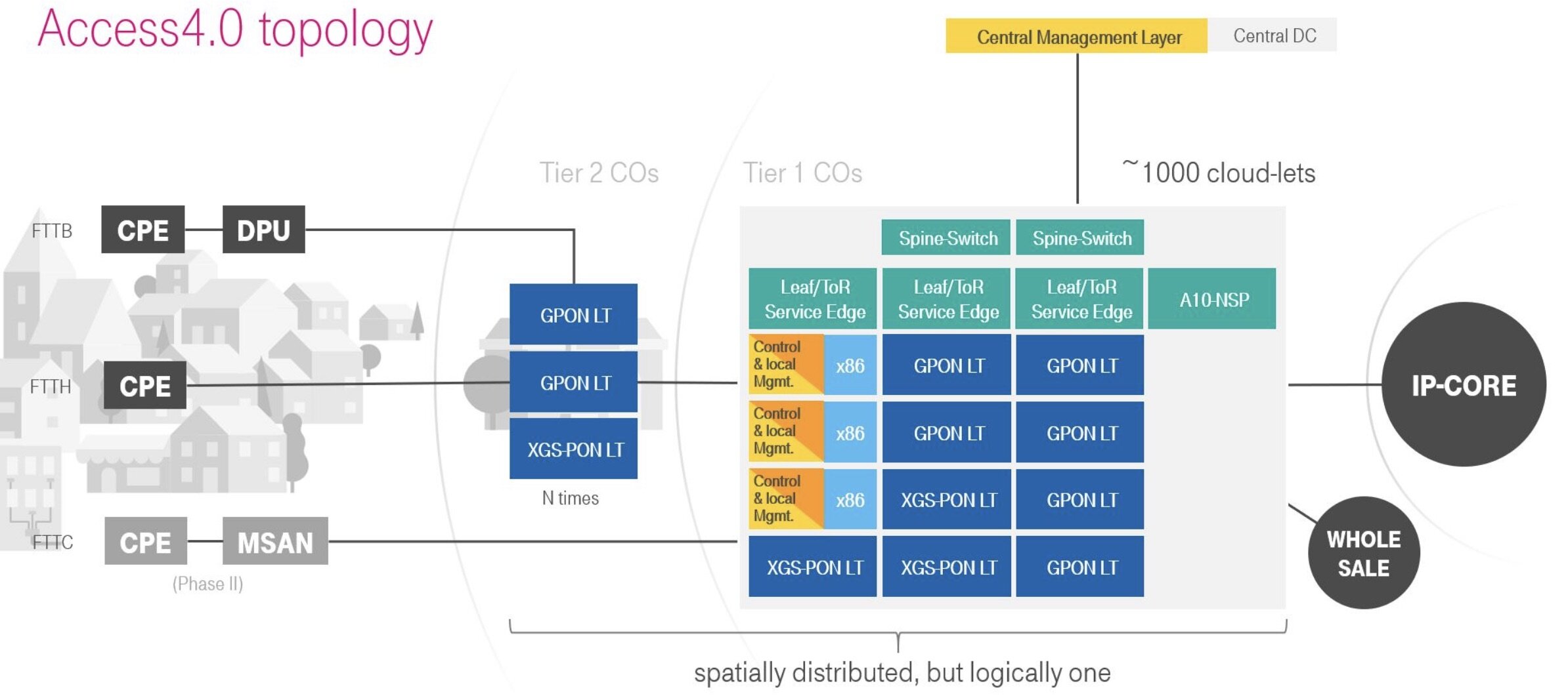
The Access 4.0 broadband deployment by Deutsche Telekom has deepened its understanding of the intricacies of network transformation. The Access 4.0 team discusses what it has learnt and reflects on the issues a mass deployment raises.
Deutsche Telekom’s Access 4.0 platform has been delivering broadband services for nearly half a year.
But the operator has deliberately limited the deployment of the next-generation fibre-to-the-x platform to one central office in Stuttgart.
Source: Deutsche Telekom
The system is fully functional, says Robert Soukup, senior program manager at Deutsche Telekom, but the operator wants to understand the processes involved so they can be automated before it starts the widescale deployment.
“Now we can see where the gaps are and what we need to adapt internally,” says Hans-Jörg Kolbe, chief engineer and head of SuperSquad Access 4.0 at Deutsche Telekom.
This will take the rest of the year. Only if this final check is successful will the Access 4.0 platform be rolled out across the operator’s 1,000 central offices in Germany.
Disaggregation
The Access 4.0 platform uses all the ingredients of network transformation: the platform is a disaggregated design running software-based network functions on white-box switches and servers as well as stackable white-box passive optical networking (PON) equipment.
The Access 4.0 programme came about after the operator conducted a detailed study of the costs involved in building networks. At the same time, the Central Office Re-architected as a Datacentre (CORD) industry initiative began.
Deutsche Telekom decided to assess CORD to determine how combining cloud technologies with access hardware would work and the possible cost benefits.
Robert Soukup
The operator quickly realised that CORD would reduce costs and once it built an Access 4.0 prototype, further cost savings and operational benefits were identified. CORD has since evolved to become the ONF’s Software Defined Networking (SDN) Enabled Broadband Access (SEBA) solution on which Access 4.0 is based.
But given its focus on networking costs, the operator hadn’t considered the far-reaching changes associated with adopting white boxes and software-hardware disaggregation, nor how a software-based architecture could shorten service introduction times. Both have since been confirmed.
Source: Deutsche Telekom
Architecture
The Access 4.0 platform uses two components developed by the Open Networking Foundation (ONF): Voltha and the SEBA reference design.
Voltha provides a common control and management system for PON white boxes while making the PON network look to the SDN controller as a programmable switch. In effect, the PON optical line terminal (OLT) is abstracted so it can be treated as a switch.
SEBA supports several fixed broadband technologies including the GPON and XGS-PON standards. Both Voltha and SEBA continue to be developed by the ONF; a Voltha version 2.7 has been announced as has a version 2.0 of SEBA.
Deutsche Telekom has now interfaced the Access 4.0 architecture to its IP core that is based on equipment from different vendors.
Challenges
Soukup stresses that a working system in the lab is very different to having a platform ready for widescale deployment.
One issue to address is security. The platform must also go through a series of planning processes and be integrated with the telco’s IT systems. Both issues were the focus of the Access 4.0 work in 2020.
“In the lab, all the wiring, cabling and planning doesn’t have to be documented that much,” says Soukup. But a field deployment requires the involvement of many staff in Deutsche Telekom’s infrastructure organisation.
“Each is responsible for a certain piece that you need in your chain, and they need to be aligned to get the maximum outcome,” says Soukup.
The Stuttgart deployment uses DT’s business support system/operations support system (BSS/OSS) stack without needing any tweaks but it is still highly manual. “This year we want to learn to do the processes right and then automate,” says Soukup. “There is a zoo of microservices in there that need to be managed and tested.”
Cloud-native
The ONF’s Voltha framework is a cloud-native design that uses containers and microservices which Deutsche Telekom has embraced for its own SDN control framework, what it calls PAO (POD access orchestrator). “Voltha is just the tip of the iceberg,” says Soukup. “The PAO is the heavy thing above and is the orchestrator that uses Voltha for the OLT/ONU.”
“We have a microservice approach, we use Docker containers and it is run on a distributed Kubernetes platform,” says Kolbe. “It allows us to slice the problem into digestible units.”
The POD’s business processes, written by the operator, also use microservices. The approach has an inherent messaging system whereby a microservice takes a message, acts on it, and returns it before being picked up by another microservice. “By doing so, you can implement any kind of business logic,” says Kolbe.
Orchestration, automation and OSS
The orchestration of the service at the point of delivery, as performed by the PAO SDN controller, is a local one while Kubernetes orchestrates the microservices. Deutsche Telekom is also investigating orchestration across sites but that is not a priority of the Access 4.0 work.
As for automation, first efforts didn’t work as expected. “When cloud stuff hits networking with VLANs, UDP (User Datagram Protocol) traffic, NATs (network address translations) and ACLs (access control lists); this we had to learn the hard way,” says Kolbe.
For the OSS, Deutsche Telekom has deliberate demarcation lines between process and production IT. The process IT involves the execution and management of the business processes while the production IT manages the live network.
“If you have the process and production mixed, if you have technology-specifics in the OSS, then if you replace a line card, for example, you have to amend the OSS,” says Soukup. “Access 4.0 does this differently and much smarter.”
The operator’s IT department for the fibre rollout has thus separated the technology-specific aspects from the service side, he says.
Learnings
When Access 4.0 went live late last year, intense videoconferencing calls took place each day to tackle the teething problems, and this lasted 10 days.
“One thing I realised was that whenever we ran into something, we could fix it ourselves,” says Kolbe. “Even I fixed something.”

Hans-Jörg Kolbe
Because the operator understood the system’s workings, it could solve issues, and quickly. “No calling someone and waiting for a binary to be delivered,” says Kolbe.
Soukup highlights the cost savings. “Deutsche Telekom has issued request-for-quotations (RFQs),” says Soukup. “At least for the hardware, the numbers are even lower than we anticipated.”
The Access 4.0 team also confirmed that disaggregation works. Deutsche Telekom has connected a bare metal router/ Broadband Network Gateway (BNG) from RtBrick to its IP core network. “This phone would ring if something was broken,” says Kolbe, touching his handset. “It hasn’t.”
As for SDN and microservices, the operator stresses that the system has yet to be scaled in the live network but what is deployed works end-to-end.
Network transformation
Access 4.0 has been Deutsche Telekom’s forerunner disaggregation project but now other teams are working on projects, says Kolbe, including home gateways and disaggregated routing.
Deutsche Telekom is working with Vodafone, Orange and Telefonica to promote Open RAN that disaggregates the radio access network (RAN).
“Disaggregation has become very important and Open RAN as well as 5G core are other big disaggregation topics,” says Gero Schultz, head of Supersquad Packet Core that includes 5G.

Gero Schultz
Deutsche Telekom stresses the importance of collaborating with fellow CSPs, even ones that compete in shared markets, citing Open RAN and the Telecom Infra Project (TIP) as examples.
“If we have a thought, we go to other operators and test the waters to see if they, and the vendors, are interested,” says Kolbe.
“We need to share with other operators,” adds Soukup. “We are just too small, one cog in the system.”
One issue that the Access 4.0 work has raised is that the operator has to be selective in what it chooses to do in-house.
“We have shown with Access 4.0 that a telco can go very far in what it can do,” says Soukup. “The question is: do we want to do this in-house and what is the core technology that we must keep for good?”
Deutsche Telekom is also addressing the ecosystem at key spots to make sure all the pieces it needs are available.
“There are going to be vendors, start-ups, consultants, operators, all software-driven,” says Kolbe. “The set-up is changing dramatically but there will always be these roles.”

Broadcom discusses its co-packaged optics plans
If electrical interfaces are becoming an impediment, is co-packaged optics the answer? Broadcom certainly thinks so.
One reason for the growing interest in co-packaged optics is the input-output (I/O) demands of switch chips. If the packet processing capacity of such chips is doubling every two years, their I/O must double too.

Alexis Björlin
But repeatedly doubling the data throughput of a switch chip is challenging.
Each new generation of switch chip must either double the number of serialiser-deserialiser (serdes) circuits or double their speed.
A higher serdes count - the latest 25.6-terabit switch ICs have 256, 100 gigabit-per-second serdes - requires more silicon area while both approaches - a higher count and higher speed - increase the chip's power consumption.
Faster electrical interfaces also complicate the system design since moving the data between the chip and the optical modules on the switch's front panel becomes more challenging.
Brad Booth, director, leading-edge architecture pathfinding team in Azure hardware systems and infrastructure at Microsoft, and president of the Consortium of On-Board Optics (COBO), describes the issue of electrical interfaces as a massive impediment.
"How do we move forward with what we need to keep the bandwidth-density growing on these devices?" says Booth. "That is not going to be solved with electronics anymore."
This explains why co-packaged optics is getting so much attention and why standardisation efforts have been started by COBO and by the OIF.
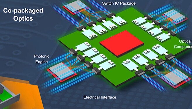
Co-packaged optics
Leading switch-chip specialist Broadcom says the relentless growth in switch-chip capacity is due to the hyperscalers' insatiable need for cross-sectional bandwidth to flatten the data centre’s networking architecture.
The hyperscalers have particular architectural needs and commonly skip a switch platform generation.
“A few hyperscalers will deploy in very large volumes a 25.6-terabit switch and either later go to 51.2 terabits or wait for 102-terabit switches to appear,” says Manish Mehta, head of product line management and strategy, optical systems division, Broadcom. “Others will be very broad with their 51.2-terabit switch deployments.”
Co-packaged optics, as the name implies, brings together optics and the chip in one package. Moving optics inside effectively creates a chip with optical I/O.
Co-packaged optics also shortens the length of the high-speed electrical links between the chip and optics, simplifying signal-integrity issues.
But co-packaged optics brings its own technical challenges. The technology also changes how data centre operators use optics and will have industry supply-chain ramifications.
Performance merits
Broadcom highlights several performance advantages using co-packaged optics.
The technology promises to reduce the power consumption by 30 per cent and the cost-per-bit by 40 per cent compared to using pluggable optics. Co-packaged optics also doubles rack density bandwidth.
Broadcom is embracing the same semiconductor techniques used for embedded memory for its on-packaged optics whereby multiple chips can be placed on a common substrate.
“We have taken a design approach that we believe can translate across multiple markets,” says Alexis Björlin, senior vice president and general manager, optical systems division, Broadcom. “Not just Ethernet switching but compute interconnects as well.”
The 30 per cent power savings is achieved by placing the optics as close as possible to the switch chip to shorten the interconnect length of high-speed electrical signals. Currently, getting the high-speed electrical signals to the pluggables requires retimer chips.
“By eliminating all that drive circuitry and putting the optics close to the chip, we are driving the optics from the serdes on the switch chip,” says Björlin. This accounts for the power savings.
The 40 per cent cost-per-bit saving is due to miniaturisation, the removal of retimers, and the improved yield using semiconductor manufacturing techniques for co-packaging.
The doubling in switch rack density using co-packaged optics is because a 51.2-terabit switch will fit in a single rack unit (1RU) box. A 25.6-terabit 1RU box is possible with pluggables.
Pluggable and co-packaged optics
Broadcom expects co-packaged optics to complement pluggable modules; it does not yet see a point where switch designs will only be possible using co-packaged optics.
"But we do know that consumption happens based on cost and power," says Björlin. "We believe there is a huge value proposition for co-packaged optics."
The merits of co-packaged optics also strengthen with each doubling of electrical interface speed. The latest 25.6-terabit switch chips use 100-gigabit serdes and the OIF has started work on a 224-gigabit electrical interface.
The power savings and optical performance co-packaged optics brings will enable new data centre architectures, says Mehta. For example, collapsing the top-of-rack layer or not having to reduce the number of platforms in a rack with each new switch because of their rising power consumption and the fact that a data centre can supply only so much power to a rack.

Manish Mehta
"Power is what is driving a lot of the investment and interest [in co-packaged optics]," says Mehta. "Cost has to hit the points necessary for adoption and deployment but power is the driver."
Ecosystem issues
One key benefit of optical modules for the data centre operators is its broad ecosystem; the operators value multiple sources and competitive pricing.
With co-packaged optics, only a few key switch-chip companies - Intel, Cisco and Broadcom among them - can deliver a complete co-packaged design. This runs counter to what the hyperscalers like.
"Publicly it may appear there are only a few companies that can provide co-packaged optics solutions," says Mehta. "But if you strip it back, there is a very broad ecosystem that is required to deliver that to market."
These include wafer fabs, packaging, and optical assembly and test companies, he says, adding that in this respect, it is similar to the optical module ecosystem.
"In the end, the hyperscalers providing infrastructure-as-a-service are monetising computing and storage; the network is an overhead," says Björlin. "We need to provide the value to reduce that overhead, and co-packaged optics technologies provide that."
Roadmap
Broadcom says it is not just addressing the switch-chip market; its optical interconnect design is being developed for disaggregated designs, compute clusters and storage. "We are all looking at this as the next generation of optical I/O to interconnect disaggregated resources," says Björlin.
The company has yet to announce a co-packaged product but in a presentation it gave at a JP Morgan event earlier this year, it outlined three upcoming designs.
First, however, it will combine its 8x100-gigabit 4-level pulse-amplitude modulation (PAM4) digital signal processor (DSP) and its silicon photonics for use in 800-gigabit pluggables. "This is a new technology and we want to bring it to market," says Björlin.
This will be followed by its co-packaged optics products codenamed Humboldt, Bailly and Janssen.
Humboldt will be a 25.6-terabit design while Bailly will be a 51.2 terabit one. Humboldt will be offered as a combination design, with different mixes of electrical and optical interfaces. "It's a single switch that you can use in any configuration," says Björlin.
Bailly will be a design with optical interfaces only. The two designs will appear either side of 2023.
Janssen is Broadcom's optical chiplet design for different types of ASICs that need optical I/O. "We have this in 800-gigabit increments," says Björlin. This will appear later on as the market isn't ready for such devices.
The next six-to-nine months will involve a lot of testing in the lab, says Mehta.
Broadcom announces products when they are sampling, so why is the company detailing its optical roadmap now?
Björlin explains that Broadcom is a platform company and this development involves working across multiple company divisions. It is important that Broadcom shares its work given how co-packaged optics involves changes in the ecosystem.
The company has increased significantly its R&D investment in the last decade. "Part of that R&D investment is to share areas of technologies which we believe will be very important in networking," says Björlin.
COBO adds co-packaged optics to its agenda

Source: COBO
The Consortium of On-Board Optics (COBO) is progressing with its work to create specifications for co-packaged optics.
The decision to address co-packaged optics by an organisation established to promote on-board optics reflects the significant industry interest co-packaged optics has gained in the last year.
So says Brad Booth, director, leading-edge architecture pathfinding team in Azure hardware systems and infrastructure at Microsoft.
The COBO work also complements that of the OIF which has set up its own co-packaged optics framework.
“We have a different collection of members [to the OIF],” says Booth. “Our members are very strong on optical connectivity and materials whereas the OIF is known for its electrical interface work and module activities like 400ZR.”
Booth has no concerns that the two groups’ specification work will overlap. The organisations have a history of working together and the head of each co-packaged optics activity is active in both COBO and the OIF.
Specification work
The COBO working group’s first output will be a white paper addressing co-packaged optics’ connectivity and thermal issues. This will be followed by specifications required in these areas.
Booth says much work will be needed to specify co-packaged optics. Booth can list 12 possible specification items that would be needed to create an interoperable ecosystem.
Some of the specifications already exist. “A lot of people are referencing the OIF CEI-112G XSR specification for the electrical interface,” says Booth. “There are also discussions about a second-generation interface which may be a different, more analogue-style interface, what some call direct-drive.”
The OIF has taken on the electrical-mechanical work given it is critical for the optical chiplet definition.
COBO has initiated external laser source specification work due to the close ties to the optical fibre and connectors work already being done by COBO's CPO working group.
“We will be having a lot of conversations with our colleagues in the OIF, and with the IEEE regarding their Ethernet specification work,” says Booth.
That is because co-packaged optics increase significantly the bandwidth-density using an optical chiplet compared to what is possible with an optical module.
“People are working on vertically integrated solutions but that doesn’t help the end-user because we may want different optics than what they make, or a different switch engine,” says Booth.
The goal is for co-packaged optics to have the same openness that exists today when building systems, having a multi-vendor choice regarding the chips and optics used.
The co-packaged work will also specify optical connectivity and external lasers issues.

Brad Booth
Interoperable co-packaged optics need not use external lasers, says Booth. But when using built-in lasers, it is not a critical concern to create a specification since there is no exposed connector.
With an external laser, however, a fibre goes from the laser source to inside the package and how that is done must be specified.
Applications
Co-packaged optics is expected to be adopted in such applications as Ethernet switches, Ethernet network interface cards (NICs), Infiniband switches and compute fabrics for artificial intelligence and supercomputing.
Ethernet switches are the main focus due to the industry facing a bandwidth-density issue associated with switch silicon.
“That is the first foray, the beachhead, for figuring out how to do co-packaged optics but it’s not the endpoint,” says Booth.
On-board optics
COBO was created to make on-board optics interoperable. Here, optics is embedded on a board to be closer to the ASIC, shortening the printed circuit board’s (PCB) electrical traces and freeing the front panel from pluggables.
COBO was backed by Microsoft and was promoted as an important intermediate step in the evolution from pluggable modules to co-packaged optics.
“The focus has moved more towards co-packaged optics,” admits Booth. “Although what is interesting is that Facebook did an on-board optics platform, and Microsoft did, and we got learnings from that.”
Facebook’s on-board optics is sourced from a company and is not COBO-complaint.
Microsoft could also have chosen a proprietary solution but it wanted to avoid being dependent on a single-source solution, given its unit requirements would be much greater.
Booth says companies are starting to build and deploy on-board optics partly because it is a valuable learning curve before moving to co-packaged optics, ‘on-board optics on steroids’ as Booth calls it.
For Microsoft, developing an on-board optics proof-of-concept platform provided valuable knowledge that it is now taking into co-packaged optics. “The beauty of creating the on-board optics specification is at least we have a standardised way to approach this.”
Once co-packaged optics gets adopted, people may think on-board optics will no longer be needed, he says. But co-packaged optics doesn’t solve everything. “It doesn’t do long-haul, or metro data centre interconnect links that Microsoft uses, such as 400ZR,” he says.
Given the higher speed of the electrical interfaces used by next-generation coherent interfaces, the trace lengths on the PCB will shrink. On-board optics will then become more attractive than faceplate optics.
In contrast, with co-packaged optics, the optics is embedded. A different co-packaged optics is needed for metro links than for use within the data centre. “Is there value in that?” says Booth. “That is a question that still needs to be answered.”
The work for interoperable on-board optics is now done. Pluggable modules such as the QSFP-DD and OSFP may support 400 gigabit and soon 800-gigabit but, with each speed hike, power and signal integrity issues worsen.
For example, 400-gigabit QSFP-DDs consume 10-14W but at 800 gigabit the power approaches 20W. That equates to a module case temperature of 70oC. That makes working and replacing pluggables an issue.
“If we had faceplate pluggables and the only other option was co-packeged optics and we had to wait for that to solve what pluggables can’t do, we as an industry would be in serious trouble,” he says.
Microsoft had designs based on COBO optics but the Azure networking team decided to use QSFP-DD for 400-gigabit, primarily because of 400ZR.
“Does that mean we have backed away from on-board optics?” says Booth. “If I talk to my sourcing team, its position is no."