
Open Eye MSA offers an alternative to PAM-4 DSPs
A group of companies, led by Macom and Semtech, have launched a multi-source agreement (MSA) to offer an alternative to using a digital signal processor (DSP) in high-speed client-side optical modules.The Open Eye MSA is developing a set of specifications for optical modules that use 50-gigabit 4-level pulse-amplitude modulation (PAM-4) signals whereby only analogue clock and data recovery (CDR) circuitry is required at the receiver.
By using the CDR instead of a PAM-4 DSP, the optical module will consume less power, have lower latency and be less costly to make, says the MSA.
To ensure interoperability, however, module makers using a PAM-4 DSP will need to meet the new MSA specification.
MSA motivation
The IEEE’s 50-gigabit PAM-4 specification was created several years ago before hardware existed, says Marek Tlalka, director of product marketing, high-performance analogue at Macom.
The IEEE specifications assumed that the received signal would be severely distorted such that the ‘eyes’ would be closed when sampled and displayed on an oscilloscope. Recovering the transmitted 4-level encoded signal would thus be a challenge.
“They had to plan for the worst-case transmitters and receivers which, in the end, led them to define the specifications such that a DSP would be required for signal recovery,” says Tlalka.
Marek Tlalka, MacomBut what has transpired is that the transmitters and receivers now used in high-speed modules have much better optical performance than originally anticipated. “You can get a nice eye on the receive side such that an analogue CDR is quite capable of the recovery,” says Tlalka.
Both Semtech and Macom, which already have such CDR solutions, went independently to their customers to promote such PAM-4 DSP-free module designs. The customers responded favourably to the claimed power, cost and latency savings, but the two companies were told that a standard was needed to generate industry backing and ensure wide availability of components and modules.
The led Macom and Semtech to found the MSA which now has 19 members. And since announcing the MSA in May, some 20 companies have enquired about joining. The companies include systems vendors, module makers, chip, and test companies.
The MSA’s current focus is on 50, 100, 200 and 400-gigabit single-mode module designs that have a reach of 500m to 2km. A draft specification, which involves the optical transmitter and receiver, is almost done, and the final version will be published in the autumn.
The MSA work will then address multi-mode module designs with the final phase tackling 100-gigabit PAM-4 (see table above).
Coexistence
The Open Eye MSA expects PAM-4 DSP modules to co-exist with its own modules.
“We want to be clear that we are not excluding DSPs,” says Timothy Vang, vice president marketing and applications at Semtech. “In this MSA spec, the analogue solution may have a power and a latency advantage, that is all.”

Timothy Vang, Semtech
Moreover, there are interface applications where a PAM-4 DSP chip will be needed. One example is for longer reaches, for data centre interconnect up to distances of 80km that are not coherent-based.
Another is for applications where a ‘gearbox’ function is used to translate the electrical signal speeds, for example, from 25-gigabit non-return-to-zero (NRZ) to 50-gigabit PAM-4, or 50-gigabit PAM-4 to 100-gigabit PAM-4.
Issue of interoperability
Tlalka stresses that what the Open Eye MSA is doing is tightening the specification of the module’s optical transmitter: “That open eye can be recovered with an analogue CDR, it can also be recovered with a DSP.”
Inphi, a maker of PAM-4 DSP chips, says it has no current plans to join the Open Eye MSA.
Eric Hayes, senior vice president, networking interconnect at Inphi, agrees that with a wide-open eye, a DSP-based optical module will be compliant with the MSA. He also points out that with an open eye, less signal processing will be required and hence the power consumption will be less.

Eric Hayes, Inphi
DSP-based modules using older laser technology, however, may be IEEE compliant but not pass the Open Eye specification. “That is where you potentially have interop issues,” says Tlalka.
“What we believe is going to happen is that the DSP module makers will just have to modify the test procedure for their modules and they will become compliant,” says Tlalka.
Inphi says the current testing procedure for DSP-based optical modules that are IEEE compliant is simple and cost-effective.
“TDECQ-compliance measurement is a highly effective yet simple quantitative procedure already supported by all test equipment,” says Hayes. TDECQ - the transmitter dispersion eye closure, quaternary - is the test used for PAM-4 rather than a traditional eye mask used for NRZ signals.
By removing the TDECQ requirement and using an eye mask to measure the PAM-4 received eye, the Open Eye MSA is forcing optical transceiver module makers to have to implement an extra layer of testing, adding cost, says Hayes.
Tlalka says the MSA does not expect the PAM-4 DSP module makers to adopt two test procedures, nor will two be necessary. “They will just have to test once [using the Open Eye test procedure],” he says.
There are already test companies as part of the Open Eye consortium and two more are joining as part of the 20 companies that have expressed an interest in joining the MSA.
Hyperscalers' preference
Inphi claims that the hyperscalers have a preference for PAM-4 DSP-based modules. This is also a view shared by Dale Murray, principal analyst at LightCounting, the market research firm.

Dale Murray, LightCounting
“We do see that hyperscalers prefer to stay with DSP-based modules,” says Hayes. “With DSP-based modules, hyperscalers and their supply chains can take advantage of lower bandwidth optics, which is already in high volume production for several years.”
DSP-based solutions also provide value to customers, such as diagnostics, health and performance monitoring, and firmware upgrades in the field. “These features could lower the total cost of ownership for the hyperscalers and reduce the operational expenditure,” says Hayes.
“I think they are going to go with what is the cheapest and lowest power,” counters Tlalka. “A generic statement is easy to make that they will stay with what is out there, but if they start getting modules that are tens of per cent lower cost and tens of per cent lower power, I think they will pretty quickly change their minds”
“We heard from the end users what they wanted the technology to enable in terms of latency, power and cost,” adds Semtech’s Vang. “We are hopefully being responsive as an ecosystem to the big data centre market.”
“At the end of the day, it will be up to the MSA players to make Open Eye a success,” says LightCounting's Murray.

ONF’s published reference designs start to be deployed
Operators are already deploying the first reference designs published by the Open Networking Foundation (ONF). Three of the ONF’s five reference designs have now been made public.
Just over a year ago, eight operators - AT&T, Comcast, China Unicom, Deutsche Telekom, Google, NTT Group, Telefonica and Turk Telekom - took the step to design key components of their edge and access networks after becoming frustrated with what they perceived as foot-dragging by the systems vendors.

AT&T is deploying one of the reference designs - the SDN-enabled broadband access scheme (SEBA). Deutsche Telekom and Telefónica have also said they will deploy SEBA during 2019 and 2020.
Andrew Fuetsch, president AT&T Labs and CTO of AT&T, said in a keynote talk at the recent Open Networking Summit North America event that SEBA is resulting in more commoditised hardware solutions and that such open source solutions are bringing higher speeds and better services across AT&T’s wireline infrastructure.
Meanwhile, an undisclosed operator has deployed a second reference design - Trellis, a leaf-spine switch fabric that supports network functions virtualisation (NFV). Trellis can be deployed as part of SEBA although the operator is deploying it for a different application, says the ONF.
The final of the three published reference designs is the Open Disaggregated Transport Network (ODTN). However, unlike SEBA and Trellis, ODTN is not yet available as a deployable platform, what ONF calls an exemplar platform.
Reference designs
The ONF started developing four reference designs as part of the open source organisation’s ongoing cloud optimised remote data centre work, known as CORD. In addition to SEBA, Trellis and ODTN, it is developing a next generation software-defined networking (NG-SDN) solution, previously known as Unified, Programmable & Automated Network (UPAN).
In February, the ONF announced a fifth reference design dubbed Converged Multi-Access and Core (COMAC) that combines 5G mobile and fixed access.
A reference design defines the assembly of components used for key platforms in the access and edge of the network. By creating reference designs, the operators are defining what they need while also committing to deploy the resulting solutions in their networks. This gives the vendors working alongside the operators a confidence that the work will lead to sales.
The components making up a reference design may be ONF-developed but need not be. They may also be open-source or a vendor-specific solution.
In parallel, the ONF operators have been working with vendors to develop an exemplar platform that is a working implementation of a reference design. The ONF only publishes a reference design once the specification is complete and the associated exemplar platform is ready for trialling. However, the ODTN reference design work is an exception in being published while its exemplar platform is unfinished.
“The ONF board felt the work was substantial and mature enough that it was worth getting out there,” says Timon Sloane, the ONF’s vice president of marketing and ecosystem.
CORD evolution
The ONF is known for its software-defined networking (SDN) work - the OpenFlow protocol and ONOS open-source SDN controller - and for its CORD open networking access and edge projects.
Originally known as the Central Office Re-architected as a Data Centre, CORD comprises two key initiatives: a broadband residential CORD (R-CORD) and a mobile CORD (M-CORD). “Once we had the foundation [of SDN], we created R-CORD, the first incarnation, and then we did M-CORD for the mobile space,” says Sloane.
The ONF has since disaggregated both M-CORD and R-CORD into their access and core components. “We realised they both covered a pretty big space,” says Sloane.
R-CORD has been disaggregated into the SEBA reference design and VOLTHA, an open-source abstraction of broadband hardware. Meanwhile, M-CORD has been split into Open Radio Access Network (ORAN) and a newer project, the Open Mobile Evolved Core (OMEC).
The ONF has also upgraded Trellis to not only provide a leaf-spine architecture switch fabric for inside a data centre but also as a multi-tier architecture that spans sites.
Meanwhile, the ODTN reference design is based on first a point-to-point and then a multi-point dense WDM (DWDM) scheme that connects the CORD edge to the network core.
The ONF has been working with the Telecom Infra Project’s (TIP) Open Optical Packet Transport group with a view to using its Cassini white box platform.
“CORD has grown in scope and we recognised that people want to consume the inner pieces in separate ways and that they have separate value,” said Sloane. “And everything of CORD ride on the SDN stack that is being gracefully migrated to the next generation SDN.”
The SDN software stack is based on the ONF’s Stratum project and the P4 language, which is now under the ONF’s stewardship. Stratum provides a software layer that supports various application programming interfaces (APIs) and the underlying hardware. The Stratum project started in 2018 and builds on software provided by Google. In addition, the ONF is also developing a micro-service ONOS.
The newest reference design, COMAC, creates a unified converged access for the radio access network and broadband, says Sloane.
First, the various elements of the fixed and mobile network access and core elements are disaggregated before convergence will bring a common framework for both. For example, a single subscriber management system for users will be used whether they are connected over broadband or mobile. This is a sophisticated project and will be developed in line with the work of the 3GPP and Broadband Forum organisations, says the ONF.
“We expect this migration to [COMAC to] be smooth but to enable a whole new set of capabilities for all the applications that run above it,” says Sloane.
Each time a new reference design is created within the ONF, it means operators committing yet more staff from different parts of their organisation to fulfil the project, says Sloane: “Additional people to pursue yet another angle of attack to transform and push their networks forward.”
Next steps
The ONF has started working on version 2.0 releases for SEBA, Trellis and the ODTN reference designs.
“This will be the case for some time as the work matures,” says Sloane. “There will be versions under development for the foreseeable future.”
Operators have a ‘bunch of work’ they want to progress and drive via this work, he says: “We don’t see an end in sight right now.”
Further information
SEBA, click here
Trellis, click here
ODTN, click here

COBO brings operational benefits to the data centre
Brad Booth admits the hyperscalers have a problem.
“Our operational inefficiencies are massive and it is only going to get worse,” says Booth, principal network architect for Microsoft’s Azure Infrastructure and chair of the Consortium for On-Board Optics (COBO).
The issue, he says, is that when a switch arrives at the data centre, it comes without the optics installed. The operations staff must unpack the optical modules, plug them into the switch and verify that each is working; an exercise that is repeated thousands of times when they commission a new data centre.
“The time it takes for us to get the network up and running impacts how quickly we can monetise the data centre,” says Booth.
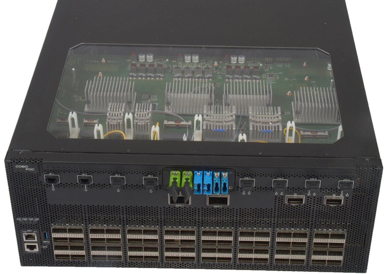
The COBO-enabled 12.8-terabit demonstrator switch. Source: COBO
Moreover, Microsoft wants to use optics to link its servers to the switches. “That is an order of magnitude more optics, which means an order of magnitude more hours,” says Booth. The sum of these hours approaches almost a year, just for the data centre’s optics.
Operational efficiencies
Booth admits that the focus of the COBO venture has been to overcome the technical challenges and publish the first release of the on-board optics specification. Only recently have the operational benefits of on-board optics become evident.
One of these benefits is that, by its very nature, the on-board optics is already installed and tested before the switch is delivered to the data centre. Booth compares on-board optics to the inveterate RJ45 Ethernet connector: “You didn't plug the RJ45 PHY layer in and then plug in the cable; it was already built into the switch.”
COBO also uses new connector designs that simplify the cleaning required when connecting the fibre to the switch.
OFC demonstrator
Microsoft, working with electronic manufacturer Delta, module maker Applied Optoelectronics, and connector suppliers Sumitomo Electric, 3M and Senko, showcased at the OFC show a demonstrator switch using COBO modules.
The proof-of-concept four-rack-unit switch uses Broadcom’s 12.8-terabit Tomahawk 3 Ethernet switch chip (see picture). The top part of the demonstrator switch has been modified to incorporate four 8-lane COBO modules, four 16-lane COBO modules and the new connector types. The switch’s front panel also uses QSFP-DD and OSFP modules that support 400-gigabit pluggable interfaces.
As for the COBO modules, Applied Optoelectronics has developed a 400-gigabit COBO module that supports four 100-gigabit PSM4 interfaces. Other vendors are also developing COBO modules but they have yet to be disclosed. The proof-of-concept platform also offers a choice of COBO connectors from Sumitomo, 3M and Senko.
Sumitomo’s contactless connector that has an air gap when it mates. The result is a more open connector that is far simpler to clean than traditional pluggable connectors. The 3M COBO connector has two polymer faces that slide over each other to create the mate. “You just squirt a can of air [onto the surface], insert it, and you are connected,” says Booth. Meanwhile, Senko's SN connector has also been designed with easy cleaning in mind.
Such operational simplification using the connectors promises significant time savings. “We have got to start doing things smarter,” says Booth. “And COBO is enabling that to happen.”
In a separate development, Petra has developed a 16x25-gigabit 400-gigabit COBO multi-mode module that has a 300m reach. Petra is using two such modules on an FPGA card for artificial intelligence tasks. “They have 800 gigabits of bandwidth coming off what looks like a standard network interface card,” says Booth. Microsoft is also exploring using Petra's module for the switch.
At OFC, the proof-of-concept platform was not operational. Delta only received the platform two weeks before the show, fitted the COBO modules and sent it straight back untested. Delta does have tested platforms up and running, however, says Booth.
>
“By 2021, I expect Microsoft will be deploying COBO switches”
Market Status
COBO was founded in 2015 and only now is the first hardware appearing. At the time, developing 400-gigabit pluggables was seen as a significant technical challenging and there were even questions raised as to whether they would deliver the required density needed for data centre switches. Now, a range of 400-gigabit interfaces in the QSFP-DD and OSFP form factors have been announced.
Meanwhile, the topic of co-packaged optics - which brings the optics from the faceplate to reside alongside the chip in the one package - is now receiving industry attention.
Do both developments limit the COBO opportunity?
“When we did this [COBO], we knew people would be able to do a faceplate with 400-gigabit [pluggable] optics,” says Booth. “And what I only got in the last few months is the operational impact [of using COBO].”
At a panel discussion at OFC, companies said they would have 800-gigabit QSFP-DD and OSFP modules by OFC 2020. “At ECOC [in September 2019], we are going to have 800 gigabits in one of these,” says Booth, pointing to a COBO module. “We are already ahead.”
COBO modules can also support 1.6 terabit interfaces once 100-gigabit PAM4 electrical interfaces become available.
InnoLight and Huawei recently joined COBO and during OFC, four other companies - systems vendors and module makers - told COBO they would be joining.
“By 2021, I expect Microsoft will be deploying COBO switches,” says Booth.
>
“Our operational inefficiencies are massive and it is only going to get worse”
Paving the way
COBO is also paving the way to co-packaged optics, or as Booth puts it, COBO has opened up Pandora’s box.
When the idea of an interoperable on-board optics standard was first discussed, there was skepticism regarding how such modules would be serviced, how they couldn't be replaced in the field, and how the switch would need to be disabled when accessing the modules.
“All these things people were saying were correct if you had certain assumptions,” says Booth. “And that was part of the problem with our industry: we got ourselves trained to be lazy.”
But by pursuing COBO, there has been a realisation that things can be done differently such as the new style of connectors.
“By cracking that open, COBO has started a more serious discussion about co-packaged optics because now we have moved the optics away from the faceplate.”

Lumentum completes sale of certain datacom lines to CIG
Brandon Collings, CTO of Lumentum, talks CIG, 400ZR and 400ZR+, COBO, co-packaged optics and why silicon photonics is not going to change the world.
Lumentum has completed the sale of part of its datacom product lines to design and manufacturing company, Cambridge Industries Group.

The sale will lower the company's quarterly revenues by between $20 million to $25 million. Lumentum also said that it will stop selling datacom transceivers in the next year to 18 months.
The move highlights how fierce competition and diminishing margins from the sale of client-side modules is causing optical component companies to rethink their strategies.
Lumentum’s focus is now to supply its photonic chips to the module makers, including CIG. “From a value-add point of view, there is a lot more value in selling those chips than the modules,” says Brandon Collings, CTO of Lumentum.
400ZR and ZR+
Lumentum will continue to design and sell line-side coherent optical modules, however.
“With coherent, there is a lot of complexity and challenge in the module’s design and manufacture,” says Collings. “We believe we can extract the value we need to continue in that business.”
The emerging 400ZR and 400ZR+ are examples of such challenging coherent interfaces.
The 400ZR specification, developed by the Optical Internetworking Forum (OIF), is a 400-gigabit coherent interface with an 80km reach. The 400 gigabit-per-second (Gbps) line rate will be achieved using a 64-gigabaud symbol rate and a 16-QAM modulation scheme.
>
“[400ZR] is not client-side. Sixty-four gigabaud is very hard to do in such an extremely compact form factor.
”
Module makers will implement the 400ZR interface using client-side pluggable modules such as the QSFP-DD and the OSFP to enable data centre operators to add coherent interfaces directly to their switches.
But implementing 400ZR will be a challenge. “This is not client-side,” says Collings. “Sixty-four gigabaud is very hard to do in such an extremely compact form factor.”
First samples of 400ZR modules are expected by year-end.
The 400ZR+ interface, while not a specification, is a catch-all for a 400-gigabit coherent that exceeds the 400ZR specification. The 400ZR+ will be a multi-rate design that will support additional line rates of 300, 200 and 100Gbps. Such rates coupled with more advanced forward-error correction (FEC) schemes will enable the 400ZR+ to span much greater distances than 80km.
The 400ZR+ interface helps the developers of next-generation coherent DSP chips to recoup their investment by boosting the overall market their devices can address. “It is basically a way of saying I’m going to spend $50 million developing a coherent DSP, and the 400ZR market alone is not big enough for that investment,” says Collings.
Lumentum says there will be some additional functionality that will be possible to fit into a QSFP-DD such that at least one of the ZR+ modes will be supported. But given the QSFP-DD module’s compactness and power constraints, the ZR+ will also be implemented in the CFP2 form factor that has the headroom needed to fully exploit the coherent DSP’s capabilities to also address metro and regional networks.
400ZR+ modules are expected in volume by the end of 2020 or early 2021.
DSP economics
Lumentum will need to source a coherent DSP for its 400ZR/ ZR+ designs as it does not have its own coherent chip. At the recent OFC show held in San Diego, the talk was of new coherent DSP players entering the marketplace to take advantage of the 400ZR/ZR+ opportunity. Collings says he is aware of five DSP players but did not cite names.
NEL and Inphi are the two established suppliers of merchant coherent DSPs. Lumentum (Oclaro) has partnered with Acacia Communications to use its Meru DSP for Lumentum’s CFP2-DCO design, although it is questionable whether Acacia will license its DSP for 400ZR/ ZR+, at least initially.
>
“God forbid if 10 or more players are doing this as no matter how you slice it, people will be losing [money]”
Lumentum and Oclaro also partnered with Ciena to use its WaveLogic Ai for a long-haul module. That leaves room for at least one more provider of a coherent DSP that could be a new entrant or an established system vendor that will license an internal design.
Collings points out that it makes no sense economically to have more than five players. If it takes $50 million to tape out a 7nm CMOS coherent DSP, the five players will invest a total of $250 million. And if the investment cost for the module, photonics and everything else is a comparable amount, that equates to $500 million being spent on the 400-gigabit coherent generation.
As for the opportunity, Collings talks of about a total of up to 500,000 ports a year by 2020. That equates to an investment return in the first year of $1,000 per device sold. “God forbid if 10 or more players are doing this as no matter how you slice it, people will be losing [money].”
Beyond Pluggables
The evolution of optics beyond pluggables was another topic under discussion at OFC.
The Consortium of On-Board Optics (COBO), the developerof an interoperable optical solution that embeds optics on the line card, had a stand at the show and a demonstration of its technology. In turn, co-packaged optics, the stage after COBO in the evolution of optical interfaces that will integrate the optics with the silicon in one package, is also now also on companies' agenda.
Collings explains that COBO came about because the industry thought on-board optics would be needed given the challenge of 400-gigabit pluggables meeting the interface density needed for 12.8-terabit switches . “I shared that opinion four to five years ago,” he says, adding that Lumentum is a member of COBO.
>
“That problem is real. It is a matter of how far the current engineering can go before it becomes too painful.”
But 400-gigabit optics has been engineered to meet the required faceplate density, including ZR for coherent. As a result, COBO is less applicable. “That need to break the paradigm is a lot less,” he says.
That said, Collings says COBO has driven valuable industry discussion given that the data centre is heading in a direction where 32 ports of 800-gigabit interfaces will be needed to get data in and out of next-generation, 25-terabit switches.
“That problem is real,” says Collings. “It is a matter of how far the current engineering can go before it becomes too painful.” Scaling indefinitely what is done today is not an option, he says.
It is possible with the next generation of switch chip to simply use a two-rack-unit box with twice as many 400-gigabit modules. “That has already been done at the 100-gigabit generation that lasted longer because it doubled up the 100-gigabit port count,” he says.
“In the generation after that, you are now asking for stuff that looks very challenging with today’s technology,” he says. “And that is where co-packaging is focused, the 50-terabit switch generation.” Switches using such capacity silicon are expected in the next four years.
But this is where it gets tricky, as co-packaging not only presents significant technical challenges but also will change the supply chain and business models.
Collings points out that hyperscalars do not like making big pioneering investments in new technology, rather they favour buying commodity hardware. “They don’t like risk, they love competition, and they like a healthy ecosystem,” he says.
“There is a lot of talk from the technology direction of how we can solve this problem [using co-packaged optics] but I think on the business side, the riskside, the investment side is putting a lot of pressure on that actually happening,” says Collings. “Where it ends up I don’t honestly know.”
Silicon photonics
One trend evident at OFC was the growing adoption of silicon photonics by optical component companies.
Indeed, the market research firm, LightCounting, in a research note summarising OFC 2019, sees silicon photonics as a must-have technology given co-packaged optics is now clearly on the industry’s roadmap.
However, Collings stresses that Lumentum’s perspective remains unchanged regarding the technology.
“It’s a fabless exercise so we can participate in silicon photonics and, quite frankly, that is why a lot of other companies are participating because the barrier to entry is quite low,” says Collings. “Nevertheless, we look at silicon photonics as another tool in the toolbox: it has advantages in some areas, some significant disadvantages in others, and in some places, it is simply comparable.”
When looking at a design from a system perspective such as a module, other considerations come into play besides the cost of the silicon photonics chip itself. Collings cites the CFP2 coherent module. While the performance of its receiver is good using silicon photonics, the modulator is questionable. You also need a laser and a semiconductor optical amplifier to compensate for silicon photonics higher loss, he says,
The alternative is to use an indium phosphide-based design and that has its own design issues. “What we are finding when you look at the right level is that the two are the same or indium phosphide has the advantage,” says Collings. “And as we go faster, we are finding silicon is not really keeping up in bandwidth and performance.”
As a result, Lumentum is backing indium phosphide for coherent operating at 64 gigabaud.
“A lot of people are talking about silicon photonics because they can talk about it,” says Collings. “It’s not worthless, don’t get me wrong, but its success outside of Acacia has been niche, and Acacia is top notch at doing this stuff.”

Macom readies its silicon photonics platform for 400G
-
Macom has announced a laser-integrated photonic integrated circuit (L-PIC) for the 400G-FR4 standard
-
The company is also working with GlobalFoundries to use the semiconductor foundry’s 300mm wafer silicon photonics process
Vivek Rajgarhia (centre) being interviewed at OFC. Source: Macom.
Macom has detailed its latest silicon photonics chip to meet the upcoming demand for 400-gigabit interfaces within the data centre.
The chip, a laser-integrated photonic integrated circuit (L-PIC), was unveiled at the OFC show held last month in San Diego. The L-PIC implements the transmitter circuitry for the 400G FR4 2km interface standard.
Backing silicon photonics
“Five to six years ago, we saw that silicon photonics would have a key role to play in photonics and optical interconnect,” says Vivek Rajgarhia, senior vice president and general manager, lightwave at Macom.
Macom acquired several companies to gain the capabilities needed to become a silicon photonics player.
In 2014 the company paid $230 million for BinOptics which provided Macom with etched facet laser technology that plays a key role in how its L-PIC platform is assembled. Also acquired was the silicon photonics design company, Photonic Controls. In 2015 Macom added FiBest, a packaging specialist, for $60 million.
“We also have the electronics expertise to go alongside [the photonics] to provide chipset solutions,” says Rajgarhia.
>
“Today, as a photonics company, if you don’t have a play in silicon photonics, you are legacy ”
Laser-integrated PIC
The biggest challenge in silicon photonics is integrating the laser, says Rajgarhia. Coupling and aligning the laser, especially when developing optical interfaces for the high-volume data centre market, needs to be done in a cost-effective and scalable way, he says.
The L-PIC, a coarse wavelength division multiplexing (CWDM) design, tackles this by having four cavities for the lasers. “Each laser is flip-chipped and inserted into a cavity without any lens or isolator, and without active alignment,” says Rajgarhia.
The self-alignment is possible by using the etched-facet laser technology from BinOptics. “When you cleave the laser facet, the dimensional control has a lot of play - the tolerance is very high - but with an etched facet, you lithographically define the mechanical dimensions,” he says. “We create a cavity in the silicon that matches the laser’s dimensions.” Macom has also incorporated multiple alignment structures as part of its L-PIC platform to enable the self-alignment.
Macom has already developed the L-PIC for the 100-gigabit CWDM4 standard. “We started with the CWDM4 because it had four wavelengths,” says Rajgarhia. “The CWDM4 is a more challenging design [than the 100-gigabit PSM4 interface] because it requires multiplexing.”
The L-PIC has now been extended to support 100-gigabit channels, to address the DR single channel and the four-channel 400-gigabit FR4 standards. The modulator bandwidth had to be extended and the laser power is different but the approach - the platform - remains the same, says Rajgarhia.
Macom refers to the L-PIC as a smart device. The electro-absorptive modulated lasers (EMLs) used for the FR4 are uncooled. The L-PIC includes ‘structures’ in the silicon such as heaters for tuning the optical elements and photo-detectors that monitor the optical performance. Macom has developed an accompanying micro-controller that sets and controls the device using such structures.
“We have developed software which we give to customers,” says Rajgarhia. “You can type in what extinction ratio you want, what power you want and it sets that up.”
The company has also started the FR4 receiver development that will also be an integrated design with a demultiplexer and four optical receiver channels.
Macom is not saying when the L-PIC will be available. However, the company says 'meaningful demand' for 400-gigabit interfaces will start from 2021.
GlobalFoundries
Macom also announced at OFC that it is working with GlobalFoundries to use the chip maker’s 90nm silicon-on-insulator 300mm wafer processing line.
“Today, as a photonics company, if you don’t have a play in silicon photonics, you are legacy,” says Rajgarhia, adding that in order to make money, what is needed is a working solution that can scale.
“When we started developing [silicon photonics devices], we and others used research foundries to get our products ready,” says Rajgarhia. “Now, what we have announced is that we are scaling this up at GlobalFoundries.”
Macom has started the development at GlobalFoundaries’ East Fishkill fab, the former IBM Microelectronics site that has undertaken a lot of research in silicon photonics, says Rajgarhia.
GlobalFoundries recently created a process development kit (PDK) for its silicon photonics line. Now Macom is an early user of the PDK.
Last year, silicon photonics start-up, Ayar Labs, entered into a strategic agreement with GlobalFoundries, providing the foundry with its optical input-output (I/O) technology while gaining access to its 45nm silicon photonics process.