
Xilinx’s Versal Premium ready for the 800-gigabit era
When Xilinx was created in 1984, the founders banked on programmable logic becoming ever more attractive due to Moore’s law.
Making logic programmable requires extra transistors so Xilinx needed them to become cheaper and more plentiful, something Moore’s law has delivered, like clockwork, over decades.
Since then, Xilinx’s field-programmable gate array (FPGA) devices have advanced considerably.
Indeed, Xilinx’s latest programmable logic family, the Versal Premium, is no longer referred to as an FPGA but as an adaptive compute accelerator platform (ACAP).
The Versal Premium series of chips, to be implemented using TSMC’s 7nm CMOS process, was unveiled for the OFC 2020 show. The Premium series will have seven chips with the largest, the VP1802, having 50 billion transistors.
First devices will ship in the second half of 2021.
ACAP series
Xilinx unveiled its adaptive compute acceleration platform in 2018.

Kirk Saban
“It is a complete rearchitecting of our device technology,” says Kirk Saban, vice president product and platform marketing at Xilinx. “It is heterogenous by nature and has multiple types of processing engines.”
“Versal Premium is evolutionary compared with previous FPGAs that have hardened blocks for certain functions,” says Bob Wheeler, principal analyst at The Linley Group. “It is another step along a continuum, not really new.”
Six ACAP families are planned for Versal: three tailored for artificial intelligence (AI) - the AI RF, AI Core and AI Edge - and the others being the Prime, Premium and HBM (high bandwidth memory).
Only Versal AI series will have AI engines: very-long-instructing-word (VLIW) processor cores that can also be used for computational-intensive tasks such as digital signal processing.
Premium is the third Versal family to be unveiled, joining the AI Core and Prime series.
Versal Prime is Xilinx’s broadest series in the portfolio, featuring a range of device sizes and capabilities. The Prime series is suited to such applications as storage acceleration in the data centre; wired networking such as 5G back-, mid- and front-haul, and passive optical networking; and industrial applications such as machine vision.
Networking needs
Versal Premium has been developed with core networking and data centre acceleration applications in mind.
“The top-end SKU handles high-end networking applications such as optical transport and data centre interconnect as well as the most demanding signal-processing applications such as radar systems,” says Wheeler.
Xilinx defines core networking as the infrastructure beyond the radio access network. “All the wireline infrastructure is what we consider to be the core of the network,” says Saban. “Access, metro, and core networks, all together.”
When Xilinx’s designers sat down to consider the networking needs for the coming six years, they anticipated a huge capacity hike in the core network. Device numbers are set to grow tenfold with each device generating ten times more traffic.
“The bandwidth going through the wired network globally needs to grow at 50 per cent on a compound annual basis to keep pace with the number of devices being connected and the data coming through them,” says Saban.
Versal Premium will deliver three times the bandwidth and nearly twice the logic capacity of the 16nm Virtex UltraScale+ VU13P FPGA, the largest device used currently for networking and data centre applications.
“Shifts are happening that the Virtex FPGAs are not going to be able to handle,” says Saban. “The move to 400 gigabit and then 800 gigabit on the mid-term horizon, the Virtex products can’t handle that kind of throughput.”
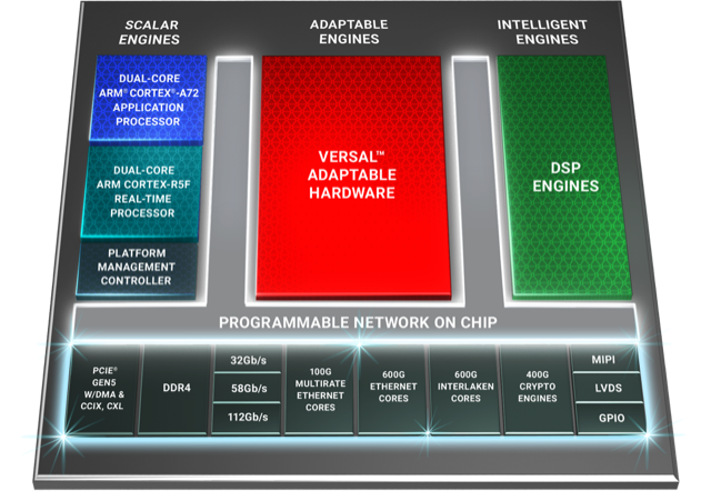
Versal Premium architecture. Source: Xilinx
Premium architecture
The Premium devices feature ARM-based scalar processors such as the dual-core Cortex-A72 application processor and the dual-core Cortex-R5F real-time processor.
The application processor is used for general-purpose processing and control. The real-time processor is used for applications that require deterministic processing. Such a processor is key for safety-certified applications.
Also included is a platform management controller that oversees the device. A user can configure many of the ACAP settings using a standard tool flow but the controller’s operation is effectively transparent to the user, says Saban.
The Premium features several types of on-chip memory that Saban likens to levels of cache memory used by high-performance processors. ”We have look-up-table RAM, Block RAM and Ultra RAM and we can offload to [external] DDR4 [RAM],” he says. “The memory hierarchy can be configured to match the algorithm you are building.”
The various on-chip functional blocks are linked via a programmable network-on-a-chip. Having the network-on-a-chip frees up programmable logic resources that would otherwise be required to connect the design’s functional blocks.
“Equipment manufacturers need to deliver on this core network growth but they also need to do it securely,” says Saban. “With everything shifting to the cloud, there are huge concerns about data privacy; in many instances, security is just as important as performance for the operators.”
To this aim, the Premium’s on-chip peripherals include 400-gigabit crypto-engines that support the AES-GCM-256 and -128, MACsec, and IPSec encryption standards.
“The crypto blocks are unique and save a lot of look-up tables and power compared with implementing these in programmable logic,” says Linley’s Wheeler.
Other on-chip features include up to 5 terabits of Ethernet throughput supporting rates from 10 to 400 Gigabit Ethernet. The devices have multiple 600-gigabit Ethernet MAC cores and support such protocols as FlexE, Flex-O, Ethernet CPRI (eCPRI), Fibre Channel over Ethernet (FCoE), and OTN.
The Premium family delivers up to 1.8 terabits of Interlaken, from 10-gigabit to 600-gigabit interfaces. Interlaken enables chip-to-chip and chip-to-backplane communications.
There are also 112-gigabit 4-level pulse-amplitude modulation (PAM-4) serialisers/ deserialisers (serdes). The VP1802 will have 28, 32-gigabit serdes and either 140, 58-gigabit or 70, 112-gigabit serdes. The electrical transceivers can drive 10m of copper cable, says Saban.
PCI Express Generation 5.0, enabling direct memory access and cache-coherent interconnect, is also supported on-chip. “We can connect to server CPUs and be an extension of their memory map,” says Saban.
Xilinx claims 22 UltraScale+ FPGAs would be needed to implement all the logic and peripherals of the Versal Premium VP1802.
System design
Wireline vendors want to double the performance with each generation of equipment while keeping platform size and power consumption constant.
Xilinx has a diagram (shown) of a generic telecom line-card design using the Versal Premium. “Vendors have different variants but at a high-level, they all look like this,” says Saban.
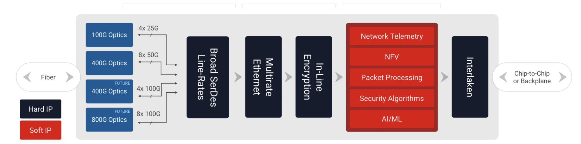
Generic telecom line card using the Versal Premium. Source: Xilinx
Line-card data arrives via optical modules. At present 100-gigabit is mainstream with 400-gigabit coming soon, and eventually 800-gigabit interfaces. The data is fed to the Premium’s hardened logic blocks: the Ethernet and encryption blocks.
The adaptive logic (in red) is what companies use to implement their unique designs such as executing virtualised network functions (NFV) or for packet processing.
“We are seeing the need to infuse artificial intelligence and machine learning into these applications in some capacity,” says Saban. Premium devices have no AI VLIW cores but have sufficient resources for some level of artificial intelligence/ machine learning capability.
Interlaken then sends the data to a host chip or across the backplane to another line card.
Software tools
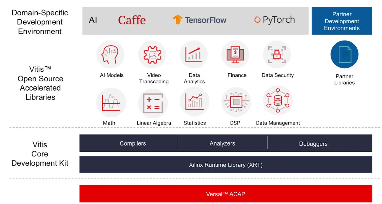
Xilinx stresses the company is no longer a chip provider but a platform provider. This is reflected in the software tools it provides to accompany its silicon.
Vitis software tool. Source: Xilinx
Versal ACAPs come with advanced toolkit libraries so engineers can program the chip with no knowledge of the underlying hardware.
Xilinx is continuing to provide its Vivado toolset that supports register-transfer level (RTL), a design abstraction used by hardware engineers for their circuit designs. “The traditional RTL toolchain is not going away and will continue to evolve,” says Saban.
But coders developing data centre applications with no knowledge of RTL or programmable logic can now use Xilinx’s Vitis toolset that was launched in 2019.
“It is critical to enable software developers and data scientists doing machine learning a way to interface to our [ACAP] products,” says Saban.
Vitis supports programming languages such as C, C++ and Python as well as higher-level machine-learning frameworks such as TensorFlow and Caffe.
Xilinx also has a library of functions for tasks such as data analytics and genomics. Such applications can be switched in and out since they are executed using adaptive hardware.
The Premium software tools will be available in the fourth quarter of the year.
Lifespan
A programmable logic family’s lifespan is five or six years; the Virtex UltraScale family was launched in 2015.
“We added a few kickers [to the Virtex family] such as high bandwidth memory and 58-gigabit serdes,” says Saban. “And we will likely do the same with Versal, add some integrated block in a derivative product.”
Xilinx’s chip designers will likely now be already working on an ACAP architecture for 2026 supporting 1.6-terabit speeds and to be implemented using a 5nm CMOS process.
“If we are to deliver twice the bandwidth at half the power, it is not enough to lean on CMOS process technology,” says Saban. “We will need to look at new chip architectures to solve the problems.”
This is challenging. “It gets harder, it gets more expensive and there are less and fewer companies that can afford it,” says Saban.

Xilinx delivers 58G serdes and showcases a 112G test chip
In the first of two articles, electrical input-output developments are discussed, focussing on Xilinx’s serialiser-deserialiser (serdes) work for its programmable logic chips. In Part 2, the Imec nanoelectronics R&D centre’s latest silicon photonics work to enable optical I/O for chips is detailed.
Part 1: Electrical I/O
Processor and memory chips continue to scale exponentially. The electrical input-output (I/O) used to move data on and off such chips scales less well. Electrical interfaces are now transitioning from 28 gigabit-per-second (Gbps) to 56Gbps and work is already advanced to double the rate again to 112Gbps. But the question as to when electrical interfaces will reach their practical limit continues to be debated.
 Gilles Garcia“Some two years ago, talking to the serdes community, they were seeing 100 gigabits as the first potential wall,” says Gilles Garcia, communications business lead at Xilinx. “In two years, a lot of work has happened and we can now demonstrate 112 gigabits [electrical interfaces].”
The challenge of moving to higher-speed serdes is that the reach shortens with each doubling of speed. The need to move greater amounts of data on- and off-chip also has power-consumption implications, especially with the extra circuitry needed when moving from non-return-to-zero signalling to the more complex 4-level pulse-amplitude modulation (PAM-4) signalling scheme.
PAM-4 is already used for 56-gigabit electrical I/O for such applications as 400 Gigabit Ethernet optical modules and leading edge 12.8-terabit switch chips. Having 112-gigabit serdes at least ensures one further generation of switch chips and optical modules but what comes after that is still to be determined. Even if more can be squeezed out of copper, the trace lengths will shorten and optics will continue to get closer to the chip.
58-gigabit serdes
Xilinx announced in March its first two Virtex Ultrascale+ FPGAs that will feature 58Gbps serdes. The company also demonstrated the technology at the OFC show. “No one else on the show floor had the same [58G serdes] capabilities in terms of bit error rate, noise floor, the demonstration across backplane technology, and transmitting and receiving data simultaneously,” says Garcia.
The two FPGAs are the VU27P that features 32 of the 58Gbps serdes as well as 32, 33Gbps serdes, while the second device, the VU29P, has 48, 58Gbps serdes as well as 32, 33Gbps ones. Both FPGA devices will ship by the year-end, says Xilinx. Moreover, customers have already used Xilinx’s 58Gbps test chip to validate its working over their systems’ backplanes in preparation for the arrival of the FPGAs.
No one else on the show floor had the same [58G serdes] capabilities in terms of bit error rate, noise floor, the demonstration across backplane technology, and transmitting and receiving data simultaneously
The Ultrascale+ FPGAs are constructed using several dice attached to a single silicon interposer to form a 2.5D chip design, what Xilinx calls its stacked silicon interconnect technology. The 58Gbps serdes are integrated into each FPGA slice. “Consider each slice as a monolithic implementation,” says Garcia.
 Source: Xilinx.
The two FPGAs with 58Gbps serdes are suited for such telecom applications as next-generation router and packet optical line cards that will use 200-gigabit and 400-gigabit client-side optical modules. The VU29P with its 48, 58Gbps serdes will be able to support line cards with up to six QSFP-DD or OSPF 400 Gigabit Ethernet modules (see the diagram of an example line card).
112-gigabit test chip
Xilinx also showcased its 112Gbps serdes test chip at the OFC show in March. “What we showed was it operating in full duplex mode - transmitting and receiving - running on the same board as the 58-gigabit serdes,” says Garcia. “The point being the 112-gigabit demo worked on a printed circuit board not designed for a 112-gigabit serdes.”
Xilinx stresses that the 112-gigabit serdes will appear on its next generation of FPGA devices implemented using a 7nm CMOS process. “It [the FPGA portfolio] will coincide with when the market needs 112 gigabits,” he says.
One obvious market indicator will be the emergence of optical modules that use electrical lanes operating at 112 gigabits. “The holy grail of optical modules is to use four [electrical] lanes for 400 gigabits,” says Garcia. The IEEE is working on such a specification and the work is expected to be completed at the end of 2019. Optical module vendors will likely have first samples in 2020. Then there is the separate timeline associated with next-generation 25.6-terabit switch chips.
“You need to have the full ecosystem before customers really implement 112Gbps serdes,” says Garcia.
Xilinx unveils a new class of compute IC
Programmable device company Xilinx has outlined an architecture that it claims represents a new class of computing chip.
The silicon architecture has been four years in the making, involved 1,500 engineers and cost over $1 billion in R&D investment.
 ACAP's functional blocks. Source: Xilinx
Dubbed the adaptive compute acceleration platform (ACAP), the first device will be fabricated using TSMC’s state-of-the-art 7nm CMOS process and will tape out later this year. The largest ACAP devices will use as many as 50 billion transistors.
“Based on the limited information from Xilinx, it is difficult to say what ACAP is, much less whether it creates a new product category,” says Linley Gwennap, principal analyst at The Linley Group.
That said, Gwennap believes the next-generation Xilinx products are far more than simply moving its FPGA technology to a 7nm CMOS. “The company has clearly put significant effort into improving the capabilities of these products to address 5G wireless, machine learning (AI), and other advanced applications,” says Gwennap.
The largest ACAP devices will use as many as 50 billion transistors
Trends
Xilinx says the relentless growth in data coupled with the emergence of artificial intelligence (AI) is driving new computing requirements. At the same time, Moore’s law is slowing down while the speed of innovation is outpacing silicon development cycles.
Victor Peng, Xilinx’s CEO, stresses that while AI is still in its infancy, the technology will be adopted across multiple industries. Thousands of applications will integrate some form of intelligence and this will occur at the network edge and in the cloud. “You will see AI end-to-end,” says Peng.
 Victor Peng
In this new era, chip architectures will be heterogeneous and use processing accelerators. “If you are going to have an intelligent, connected world, it really needs to be adaptable,” says Peng. “It needs to be adaptable because you cannot predict all the needs of the future.”
Gwennap says many companies have already delivered heterogenous chips, given the term heterogeneous refers to a mix of CPU, graphics processor unit (GPU) and digital signal processor (DSP) cores. “This includes every smartphone and PC processor shipping today,” he says.
It also is not clear what ‘adaptive’ means, adds Gwennap: “But if you interpret it to mean FPGA, then both Xilinx and Altera (now Intel) have delivered chips mixing CPUs, DSPs, and FPGAs for years.”
It configures a processor to do a job then, pffft, it has gone
ACAP
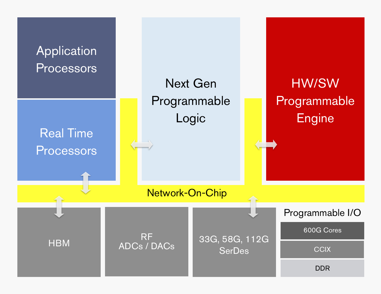
Xilinx is not yet detailing the ACAP architecture until the first devices are launched but it has listed the main architectural features.
“Overall, it can be programmed at the hardware level and it has enough architectural features that it can be programmed purely from a software perspective,” says Peng. This means that things can be changed not just at the software level but down at the hardware level, dynamically, while the device is running.
“It configures a processor to do a job then, pffft, it has gone,” says David Manners, the veteran chip journalist at Electronics Weekly who has been covering Xilinx since it was founded in the 1980s.
The ACAP architecture will include both application and real-time processors as well as programmable logic for digital signal processing (DSP) and a hierarchy of distributed memory. The chip will also feature a high-speed network-on-a-chip linking the functional blocks and arbitrating between them.
ACAP will support various generations of DDR memory and certain family devices will include high-bandwidth 3D stacked memory. There will also be device members that use RF analogue-to-digital and digital-to-analogue converters.
In turn, ACAP will have fast input-output circuitry with serial/deserialisers (SERDES) running at 33, 58 and even 112 gigabit-per-second (Gbps) rates. Xilinx demonstrated its latest 112Gbps serdes at the recent OFC show held in San Diego.
Certain ACAP devices will use a novel engine that is software and hardware programmable. Programming the engine at the software level will require some embedded expertise.
“We are always looking at how we can use our hardware programming expertise to get another level of optimisation beyond just software-programmable blocks,” says Peng. Xilinx will detail the engine’s workings later this year.
Xilinx says the 7nm ACAP will deliver a 20x AI compute performance improvement and 4x the 5G communications bandwidth compared to its current 16nm FPGAs.
The company has already delivered software tools for ACAP to select customers and expects first device shipments in 2019.
Data-centre focus
Peng, who has been CEO since January, says the data centre market is now Xilinx’s top priority segment.
Data centres require ever more computing while their networked architectures continue to evolve. This represents an attractive market for Xilinx especially given its programmable devices not only serve computing but also storage and networking requirements.
Xilinx has also been expanding its software development environments that let its devices be programmed at a higher level by developers that have little or no knowledge of the underlying hardware. This contrasts with traditional Xilinx FPGA users that by nature are hardware engineers. “There are easily 1000x more software developers than FPGA developers,” says Peng.
Companies such as Amazon, Alibaba, Huawei, Baidu, Nimbix and Tencent also offer FPGAs-as-a-service as part of their cloud offerings.
The central role of software in data centres may have caused chips to recede into the background, yet Xilinx will argue that the nature of the silicon has never been more important.
FPGAs with 56-gigabit transceivers set for 2017
The company demonstrated a 56-gigabit transceiver using 4-level pulse-amplitude modulation (PAM-4) at the recent OFC show. The 56-gigabit transceiver, also referred to as a serialiser-deserialiser (serdes), was shown successfully working over backplane specified for 25-gigabit signalling only.
 Gilles GarciaXilinx's 56-gigabit serdes is implemented using a 16nm CMOS process node but the first FPGAs featuring the design will be made using a 7nm process. Gilles Garcia says the choice of 7nm CMOS is solely a business decision and not a technical one.
”Optical module [makers] will take another year to make something decent using PAM-4," says Garcia, Xilinx's director marketing and business development, wired communications. "Our 7nm FPGAs will follow very soon afterwards.”
The company is still to detail its next-generation FPGA family but says that it will include an FPGA capable of supporting 1.6 terabit of Optical Transport Network (OTN) using 56-gigabit serdes only. At first glance that implies at least 28 PAM-4 transceivers on a chip but OTN is a complex design that is logic not I/O limited suggesting that the FPGA will feature more than 28, 56-gigabit serdes.
Applications
Xilinx’s Virtex UltraScale and its latest UltraScale+ FPGA families feature 16-gigabit and 25-gigabit transceivers. Managing power consumption and maximising reach of the high-speed serdes are key challenges for its design engineers. Xilinx says it has 150 engineers for serdes design.
“Power is always a key challenge because as soon as you talk about 400-gigabit to 1-terabit per line card, you need to be cautious about the power your serdes will use,” says Garcia. He says the serdes need to adapt to the quality of the traces for backplane applications. Customers want serdes that will support 25 gigabit on existing 10-gigabit backplane equipment.
Xilinx describes its Virtex UltraScale as a 400-gigabit capable single-chip system supporting up to 104 serdes: 52 at 16 gigabit and 52 at 25 gigabit.
The UltraScale+ is rated as a 500-gigabit to 600-gigabit capable system, depending on the application. For example, the FPGA could support three, 200-gigabit OTN wavelengths, says Garcia.
Xilinx says the UltraScale+ reduces power consumption by 35% to 50% compared to the same designs implemented on the UltrasScale. The Virtex UltraScale+ devices also feature dedicated hardware to implement RS-FEC, freeing up programmable logic for other uses. RS-FEC is used with multi-mode fibre or copper interconnects for error correction, says Xilinx. Six UltraScale+ FPGAs are available and the VU13P, not yet out, will feature up to 128 serdes, each capable of up to 32 gigabit.
We don’t need retimers so customers can connect directly to the backplane at 25 gigabit, thereby saving space, power and cost
The UltraScale and UltraScale+ FPGAs are being used in several telecom and datacom applications.
For telecom, 500-gigabit and 1-terabit OTN designs are an important market for the UltraScale FPGAs. Another use for the FPGA serdes is for backplane applications. “We don’t need retimers so customers can connect directly to the backplane at 25 gigabit, thereby saving space, power and cost,” says Garcia. Such backplane uses include OTN platforms and data centre interconnect systems.
The FPGA family’s 16-gigabit serdes are also being used in 10-gigabit PON and NG-PON2 systems. “When you have an 8-port or 16-port system, you need to have a dense serdes capability to drive the [PON optical line terminal’s] uplink,” says Garcia.
For data centre applications, the FPGAs are being employed in disaggregated storage systems that involved pooled storage devices. The result is many 16-gigabit and 25-gigabit streams accessing the storage while the links to the data centre and its servers are served using 100-gigabit links. The FPGA serdes are used to translate between the two domains (see diagram).
 Source: Xilinx
For its next-generation 7nm FPGAs with 56-gigabit transceivers, Xilinx is already seeing demand for several applications.
Data centre uses include server-to-top-of-rack links as the large Internet providers look move from 25 gigabit to 50- and 100-gigabit links. Another application is to connect adjacent buildings that make up a mega data centre which can involve hundreds of 100-gigabit links. A third application is meeting the growing demands of disaggregated storage.
For telecom, the interest is being able to connect directly to new optical modules over 50-gigabit lanes, without the need for gearbox ICs.
Optical FPGAs
Altera, now part of Intel, developed an optical FPGA demonstrator that used co-packaged VCSELs for off-chip optical links. Since then Altera announced its Stratix 10 FPGAs that include connectivity tiles - transceiver logic co-packaged and linked with the FPGA using interposer technology.
Xilinx says it has studied the issue of optical I/O and that there is no technical reason why it can’t be done. But the issue is a business one when integrating optics in an FPGA, he says: “Who is responsible for the yield? For the support?”
Garcia admits Xilinx could develop its own I/O designs using silicon photonics and then it would be responsible for the logic and the optics. “But this is not where we are seeing the business growing,” he says.
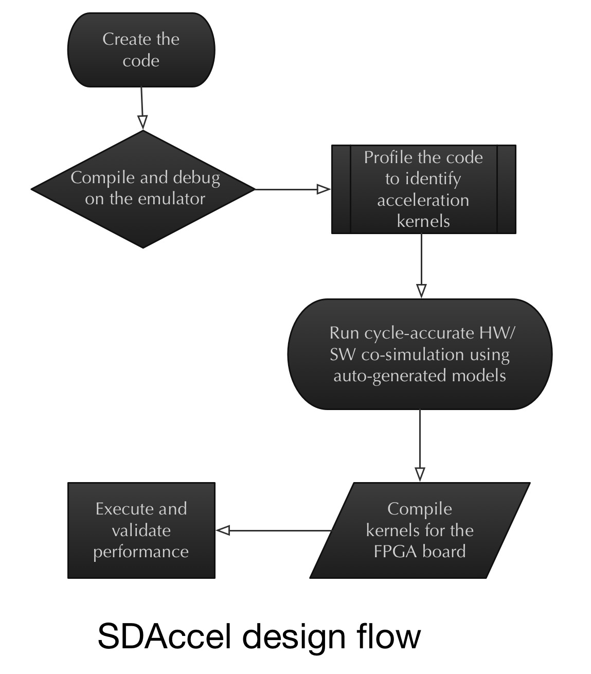
OpenCL and the reconfigurable data centre
Part 3: General purpose data centres
Xilinx's adoption of the Open Computing Language (OpenCL) as part of its SDAccel development tool is important, not just for FPGAs but also for the computational capabilities of the data centre.
The FPGA vendor is promoting its chips as server co-processors to tackle complex processing tasks such as image searches, encryption, and custom computation.
Search-engine specialists such as Baidu and Microsoft have seen a greater amount of traffic for image and video searches in the last two years, says Loring Wirbel, senior analyst at market research firm, The Linley Group: "All of a sudden they are seeing that these accelerator cards as being necessary for general-purpose data centres."
Xilinx and Altera have been way ahead of the niche FPGA vendors, indeed ahead of a lot of the network processor and graphics processor (GPU) vendors, in recognising the importance of OpenCL
OpenCL was developed by Apple and is being promoted by the Khronos Group, an industry consortium set up to promote the integration of general purpose microprocessors, graphics processors, and digital signal processing blocks. And it is the FPGA vendors that are playing a pivotal role in OpenCL's adoption.
"Xilinx and Altera have been way ahead of the niche FPGA vendors, indeed ahead of a lot of the network processor and graphics processor (GPU) vendors, in recognising the importance of OpenCL," says Wirbel.
Altera announced the first compiler kit for OpenCL in 2013. "The significant thing Altera did was develop 'channels' for accelerator 'kernels'. Using the channels, kernels - the tasks to be accelerated in hardware - communicate with each other without needing the host processor. "It offers an efficient way for multiple co-processors to talk to each other," says Wirbel. The OpenCL community have since standardised elements of Altera's channels, now referred to as pipes.
"What Xilinx has brought with SDAccel is probably more significant in that it changes the design methodology for bringing together CPUs and GPUs with FPGAs," says Wirbel. Xilinx's approach may be specific to its FPGAs but Wirbel expects other firms to adopt a similar design approach. "Xilinx has created a new way to look at design that will ease the use of parallelism in general, and OpenCL," says Wirbel. (see SDAccel design approach, below.)
"Altera and Xilinx should be saluted in that they have encouraged people to start looking at OpenCL as a move beyond C for programming everything," says Wirbel. This broadening includes programming multi-core x86 and ARM processors, where a good parallel language is desirable. "You get better performance moving from C to C++, but OpenCL is a big jump," he says.
The future says that every data centre is going to become an algorithmically-rich one that can suddenly be reallocated to do other tasks
Wirbel does not have hard figures as to how many of a data centre's servers will have accelerator cards but he believes that every data centre is going to have specialised acceleration for tasks such as imaging and encryption as a regular feature within the next year or two. His educated guess is that it will be one accelerator card per eight host CPUs and possibly one in four.
Longer terms, such acceleration will change the computational nature of the data centre. "The future says that every data centre is going to become an algorithmically-rich one that can suddenly be reallocated to do other tasks," he says. It could mean that institutions such as national research labs that tackle huge-scale simulation work may no longer require specialist supercomputer resources.
"That is a little bit exaggerated because what will really happen is you will have to have whole clusters of data centres around the country allocated to ad-hoc virtual multiprocessing on very difficult problems," says Wirbel. "But the very notion that there needs to be assigned computers in data centres to one set of problems will be a thing of the past."
How does that relate to Xilinx's SDAccel and OpenCL?
"Some of this will happen because of tools like OpenCL as the language and tools like SDAccel for improving FPGAs," says Wirbel.
The SDAccel design approach
Xilinx has adopted the concept of co-simulation at an early stage of an FPGA-based co-processor design, alongside a server's x86 processor.
Wirbel says that despite all the talk about co-simulation over the last decade, little has been done in practice. With co-simulation, an x86 processor or a graphics processor is simulated with a designer's IP logic that makes up an ASIC or an FPGA design.
Making FPGAs with very tightly-packed processors and with a very low power dissipation is critical; it is a big deal
"What Xilinx did is they said: the biggest problem is designers having to redo an FPGA, even placing and routing elements and going back to using back-end EDA [electronic design automation] tools," says Wirbel. "Maybe the best way of doing this is recognising we have to do some early co-simulation on a target x86 CPU board."
This is where OpenCL plays a role.
"The power of OpenCL is that it lets you define an acceleration task as a kernel," says Wirbel. It is these acceleration kernels that are sent to the hardware emulator with the x86 on board. The kernels can then be viewed in the co-simulation environment working alongside the x86 such that any problems encountered can be tackled, and the two optimised. "Then, and only then, do you send it to a compiler for a particular FPGA architecture."
The challenge for Xilinx is keeping a lid on the FPGA accelerator card's power consumption given the huge number of servers in a data centre.
"The large internet players have got to be able to add these new features for almost zero extra power," says Wirbel. "Making FPGAs with very tightly-packed processors and with a very low power dissipation is critical; it is a big deal."
For Part 1, click here
For Part 2, click here
What role FPGA server co-processors for virtual routing?
IP routing specialists have announced first virtual edge router products that run on servers. These include Alcatel-Lucent with its Virtualized Service Router and Juniper with its vMX. Gazettabyte asked Alcatel-Lucent's Steve Vogelsang about the impact FPGA accelerator cards could have on IP routing.

Steve Vogelsang, IP routing and transport CTO, Alcatel-Lucent
The co-processor cards in servers could become interesting for software-defined networking (SDN) and network function virtualisation (NFV).
The main challenge is that we require that our virtualised network functions (vNFs) and SDN data plane can run on any cloud infrastructure; we can’t assume that any specific accelerator card is installed. That makes it a challenge.
I can imagine, over time, that DPDK, the set of libraries and drivers for packet processing, and other open source libraries will support co-processors, making it easier to exploit by an SDN data plane or vNF.
For now we’re not too worried about pushing the limits of performance because the advantage of NFV is the operational simplicity. However, when we have vNFs running at significant scale, we will likely evaluate co-processor options to improve performance. This is similar to what Microsoft and others are doing with search algorithms and other applications.
Note that there are alternative co-processors that are more focussed on networking acceleration. An example is Netronome which is a purpose-built network co-processor for the x86 architecture. Not sure how it compares to Xilinx for networking functionality, but it may outperform FPGAs and be a better option if networking is the focus.
Some servers are also built to enable workload-specific processing architectures. Some of these are specialised on a single processor architecture while others such as HP's Moonshot allow installation of various processors including FPGAs.
When we have vNFs running at significant scale, we will likely evaluate co-processor options to improve performance
I don’t expect FPGA accelerator cards will have much impact on network processors (NPUs). We or any other vendor could build an NPU using a Xilinx or another FPGA. But we get much more performance by building our own NPU because we control how we use the chip area.
When designing an FPGA, Xilinx and other FPGA vendors have to decide how to allocate chip space to I/O, processing cores, programmable logic, memory, and other functional blocks. The resulting structure can deliver excellent performance for a variety of applications, but we can still deliver considerably more performance by designing our own chips allocating the chip space needed to the required functions.
I have experience with my previous company which built multiple generations of NPUs using FPGAs, but they could not come close to the capabilities of our FP3 chipset.
For Part 1, click here
For Part 3, click here
FPGAs embrace data centre co-processing role
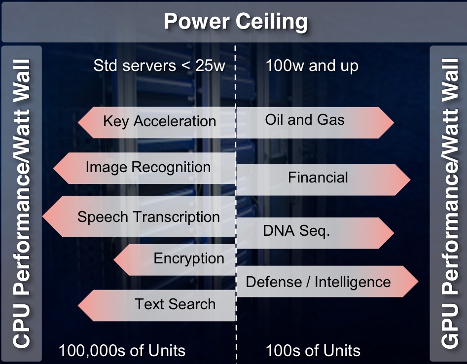 The PCIe accelerator card has a power budget of 25W. Hyper data centres can host hundreds of thousands of servers whereas other industries with more specialist computation requirements use far fewers servers. As such, they can afford a higher power budget per card. Source: Xilinx
Xilinx has developed a software-design environment that simplifies the use of an FPGA as a co-processor alongside the server's x86 instruction set microprocessor.
Dubbed SDAccel, the development environment enables a software engineer to write applications using OpenCL, C or the C++ programming language running on servers in the data centre.
Applications can be developed to run on the server's FPGA-based acceleration card without requiring design input from a hardware designer. Until now, a hardware engineer has been needed to convert the code into the RTL hardware description language that is mapped onto the FPGA's logic gates using synthesis tools.
"[Now with SDAccel] you suffer no degradation in [processing] performance/ Watt compared to hand-crafted RTL on an FPGA," says Giles Peckham, regional americas and EMEA marketing director at Xilinx. "And you move the entire design environment into the software domain; you don't need a hardware designer to create it."
Data centre acceleration
The data centre is the first application targeted for SDAccel along with the accompanying FPGA accelerator cards developed by Xilinx's three hardware partners: Alpha Data, Convey and Pico Computing.
The FPGA cards connect to the server's host processor via the PCI Express (PCIe) interface are not just being aimed at leading internet content providers but also institutions and industries that have custom computational needs. These include oil and gas, financial services, medical and defence companies.
PCIe cards have a power budget of 25W, says Xilinx. The card's power can be extended by adding power cables but considering that hyper data centres can have hundreds of thousands of servers, every extra Watt consumed comes at a cost.
Microsoft has reported that a production pilot it set up that had 1,632 servers using PCIe-based FPGA cards, achieved a doubling of throughput, a 29 percent lower latency, and a 30 percent cost reduction compared to servers without accelerator cards
In contrast, institutions and industries use far fewer servers in their data centres. "They can stomach the higher power consumption, from a cost perspective and in terms of dissipating the heat, up to a point," says Peckham. Their accelerator cards may consume up to 100W. "But both have this limitation because of the power ceiling," he says.
China’s largest search-engine specialist, Baidu, uses neural-network processing to solve problems in speech recognition, image search, and natural language processing, according to The Linley Group senior analyst, Loring Wirbel.
Baidu has developed a 400 Gigaflop software-defined accelerator board that uses a Xilinx Kintex-7 FPGA that plugs into any 1U or 2U high server using PCIe. Baidu says that the FPGA board achieves four times higher performance than graphics processing units (GPUs) and nine times higher performance than CPUs, while consuming between 10-20W.
Microsoft has reported that a production pilot it set up that had 1,632 servers using PCIe-based FPGA cards, achieved a doubling of throughput, a 29 percent lower latency, and a 30 percent cost reduction compared to servers without accelerator cards.
"The FPGA can implement highly parallel applications with the exact hardware required," says Peckham. Since the dynamic power consumed by the FPGA depends on clock frequency and the amount of logic used, the overall power consumption is lower than a CPU or GPU. That is because the FPGA's clock frequency may be 100MHz compared to a CPU's or GPU's 1 GHz, and the FPGA implements algorithms in parallel using hardware tailored to the task.
 FPGA processing performance/ W for data centre acceleration tasks compared to GPUs and CPUs. Note the FPGA's performance/W advantage increases with the number of software threads. Source: Xilinx
SDAccel
To develop a design environment that a software developer alone can use, Xilinx has to make SDAccel aware of the FPGA card's hardware, using what is known as a board support package. "There needs to be an understanding of the memory and communications available to the FPGA processor," says Peckham. "The processor then knows all the hardware around it."
Xilinx claims SDAccel is the industry's first architecturally optimising compiler for FPGAs. "It is as good as hand-coding [RTL]," says Peckham. The tool also delivers a CPU-/ GPU-like design environment. "It is also the first tool that enables designs to have multiple operations at different times on the same FPGA," he says. "You can reconfigure the accelerator card in runtime without powering down the rest of the chip."
SDAccel and the FPGA cards are available, and the tool is with several customers. "We have proven the tool, debugged it, created a GUI as opposed to a command line interface, and have three FPGA boards being sold by our partners," says Peckham. "More partners and more boards will be available in 2015."
Peckham says the simplified design environment appeals to companies not addressing the data centre. "One company in Israel uses a lot of Virtex-6 FPGAs to accelerate functions that start in C code," he says. "They are using FPGAs but the whole design process is drawn-out; they were very happy to learn that [with SDAccel] they don't have to hand-code RTL to program them."
Xilinx is working to extend OpenCL for computing tasks beyond the data centre. "It is still a CPU-PCIe-to-co-processor architecture but for wider applications," says Peckham.
For Part 2, click here
For Part 3, click here
FPGA transceiver speed hikes bring optics to the fore

Despite rapid increases in the transceiver speeds of field-programmable gate arrays (FPGA), the transition to optical has begun.
FPGA vendors Xilinx and Altera have increased their on-chip transceiver speeds fourfold since 2005, from 6.5Gbps to 28Gbps. But signal integrity issues and the rapid decline in reach associated with higher speed means optics is becoming a relevant option.
Altera has unveiled a prototype with two 12x10Gbps optical engines but has yet to reveal its product plans. Xilinx believes that FPGA optical interfaces are still several years off with requirements being met with electrical interfaces for now.
Fibre-to-the-FPGA
Part 1: FPGAs
Programmable logic chip vendor Altera is developing FPGAs with optical interfaces. But is there a need for such technology and how difficult will it be to develop?
FPGAs with optical interfaces promise to simplify high-speed interfacing between and within telecom and datacom systems. Such fibre-based FPGAs, once available, could also trigger novel system architectures. But not all FPGA vendors believe optical-enabled FPGAs’ time has come, arguing that cost and reliability hurdles must be overcome for system vendors to embrace the technology

“One of the advantages of using optics is that you haven’t got to throw your backplanes away as [interface] speeds increase.”
Craig Davis, Altera
Altera announced in March that it is developing FPGAs with optical interfaces. The FPGA vendor has yet to detail its technology demonstrator but says it will do so later this year. Altera describes the advent of optically-enabled FPGAs as a turning point, driven by the speed-reach tradeoff of electrical interfaces coupled with the rising cost of elaborate printed circuit board (PCB) materials needed for the highest speed interfaces.
Interface speeds continue to rise. The Interlaken interface has a channel rate of up to 6.375 Gigabit-per-second (Gbps) while the Gen 3.0 PCI Express standard uses 8.0 Gbps lanes. Meanwhile 16 Gigabit Fibre Channel standard operates at 14.1 Gbps while 100 Gigabit interfaces for Ethernet and line-side optical transport are moving to a four-channel electrical interface that almost doubles the lane rates to 25-28 Gbps. The CFP2 optical module for 100 Gigabit, to be introduced in 2012, will use the four-channel electrical interface.
Copper interfaces such channel speeds but at the expense of reach. Craig Davis, senior product marketing engineer at Altera, cites the 10GBASE-KR 10Gbps backplane standard as an example of the bandwidth-reach the latest FPGAs can achieve: 40 inches including the losses introduced by the two connectors at each end.

“Our interactions with our customers are primarily for products that are not going to see the light of day for several years”
Panch Chandrasekaran, Xilinx
Work is being undertaken to development very short reach electrical interfaces at 28Gbps for line cards and electrical backplanes. “You are talking 4 to 6 inches of trace to a CFP2 module or a chip-to-chip interface,” says Panch Chandrasekaran, Xilinx’s senior product marketing manager, high-speed serial I/O. “Honestly, this is going to be a challenge but we usually figure out a way how to do things.”
The faster the link, the more energy has to be put into the signals and the more losses you have on the board, says Davis: “Signal integrity aspects also get more difficult, the costs go up as does the power consumption.”
According to Altera, signal losses increase 3.5x going from 10 to 30Gbps. To match the losses at 10Gbps when operating at these higher speeds, complex PCB materials such as N4000-13 EP SI and Megtron 6 are needed rather than the traditional FR4 design. However, the cost of designing and manufacturing such PCBs can rise by five-fold.
In contrast, using an optically-enabled FPGA simplifies PCB design. “For traditional chip-to-chip on a line card, optics does have a benefit because you can trade off the number of layers on a PCB,” says Davis. Such an optical-based design also offers future-proofing. “A lot of the applications we’ll be looking to support are across backplanes and between shelves,” says Davis. “One of the advantages of using optics is that you haven’t got to throw your backplanes away as [interface] speeds increase.”
FPGAs with optical interfaces also promise new ways to design systems. Normally when one line card talks to another on different shelves it is via a switch card on each shelf. Using an FPGA with an optical interface, the cards can talk directly. “People are looking at this,” says Davis. “You could take that to the extreme and go to the next cabinet which makes a much easier system design.”
Altera says vendors are interested in optical-enabled FPGAs for storage systems. Here interlinked disk drives require multiple connectors between boards. “There is an argument that it becomes a simpler system design with one FPGA taking directly to another or one chip directly to another,” says Davis “The more advanced R&D groups within certain companies are investigating the best route forward.”
But while FPGA companies agree that optical interfaces will be needed, there is no consensus on timing. “Xilinx has been looking at this technology for a while now,” says Chandrasekaran. “There is a reason why we haven’t announced it: we have a little while to go before key ecosystem and technology questions are answered.”
The mechanical and reliability issues of systems are stringent and the optical option must prove that it can deliver what is needed, says Chandrasekaran. “It is possible to do at the moment but the cost and reliability equation hasn’t been fully solved.”
Xilinx also says that while it is discussing the technology with customers, the requirement for such FPGA-based optical interfaces is some way off. “Our interactions with our customers are primarily for products that are not going to see the light of day for several years,” says Chandrasekaran
“Customers are always excited to hear about integration play,” says Gilles Garcia, director, wired communications business unit at Xilinx. But ultimately end customers care less about the technology as long as the price, power and board real-estate requirements are met. “What we are seeing with this [optical-enabled FPGA] technology is that it is not answering the requirements we are seeing from our large customers that are looking for their next-generation systems,” says Garcia
FPGA vendor Tabula also questions the near-term need for such technology. Alain Bismuth, vice president of marketing at Tabula, says nearly all the ports shipped today are at speeds of 10Gbps and below. Even in 2014, the number of 40Gbps ports forecast will only number 650,000, he says.
For Bismuth, two things must happen before optically-enabled FPGAs become commonplace. “You can build them in high volumes reliably and with good yields without incurring higher costs than a separate, discrete [FPGA and optical module] solution,” says Bismuth. “Second, the emergence in interesting volume of networks at 100 Gig and beyond to justify the integration effort.” Such networks are emerging at a “fairly slow pace”, he says.
Meanwhile Altera’s development work continues apace. “We are working with partners to develop the system and we will be demonstrating the optics-on-a-chip in Q4,” says Bob Blake, corporate and product marketing manager, Altera Europe. Altera says its packaged FPGA and optical interface will support short reach links up to 100m and be based on multimode fibre. “All we have announced is that the optical interface will be on the package and it will connect into the FPGA,” says Davis.
The technology will also use 10Gbps optical interface yet the company has detailed that its Stratix V FPGA family supports electrical transceivers at 28Gbps. “The optical interface can go higher than that [10Gbps] so in future we can target 28Gbps and beyond,” says Davis.
Optical partners
Optical component and transceiver firms such as Avago Technologies, Finisar and Reflex Photonics all have parallel optical devices - optical engines - that support up to 12 channels at 10Gbps. Avago’s MicroPod 12x10Gbit/s optical engine measures 8x8mm, for example.
None of the optical vendors would comment on its involvement with Altera’s optical-enabled FPGA.
Avago Technologies says that as FPGA interface speeds move to 10 Gbps and beyond, its customers are finding they need to move from copper to optical interfaces to maintain bandwidth for board, chassis, and system-level interconnect. “In line with this announcement from Altera, we are investing the time to verify Avago optical modules with FPGA SERDES blocks to ensure that FPGA users can design optical interfaces with confidence,” says Victor Krutul, director of marketing for fibre optic products at Avago.
Finisar too only talks about general trends. “We are seeing many technology leaders moving optics further onto the board and deeper into the system,” says Katharine Schmidtke, director of strategic marketing for Finisar. “This approach offers a number of advantages including improving signal integrity and reducing power consumption on copper traces at higher bandwidths.”
Reflex Photonics says that it has the technology and products to realise optically-enabled IC packages. “We are working with more than one IC company to bring optically-enabled IC packages to market,” says Robert Coenen, vice president, sales and marketing at Reflex.
For Coenen, FPGAs represent the first step in bringing optics to the IC package: “Due to their penetration into niche markets, FPGAs make the most sense to create what will ultimately be a huge market in optically-enabled IC packages.”
Coenen stresses that optics to the IC package is a significant shift in how optical links are used and so it will take time for this application to take hold. However, as the cost per bit decreases, optics will start being used in additional applications including switch ASICs, microprocessors and graphics processors.
“The beauty of an MT-terminated ribbon fiber optical connection at the edge of the package is that this solution allows designers to use the additional high-speed optical connectivity without having to drastically change their design practices,” says Coenen. This is not the case with technologies such as PCB optical waveguides or free-space optical communication.
“I believe the Altera announcement is just the first in what will be many announcements of optical-to-the-IC-package technology in the coming year or two,” says Coenen.
Further reading
- Briefing Part 2: Boosting high performance computing with optics
- Altera White Paper: Overcome Copper Limits with Optical Interfaces
- Xilinx's 400 Gigabit Ethernet FPGA
- The InfiniBand roadmap gets redrawn
Xilinx's 400 Gigabit Ethernet FPGA
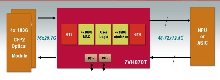 A single FPGA will support 400 Gigabit Ethernet duplex traffic. The FPGA can also support 4x100Gig MACs and 4x150Gbps Interlaken interfaces. Source: Xilinx
Why is it important?
Xilinx says its switch and router customers are more than doubling the traffic capacity of their platforms every three years. “They are looking for silicon that will support a doubling of capacity within the same form-factor and the same power budget,” says Giles Peckham, EMEA marketing director at Xilinx.
An FPGA has an advantage when compared to an application-specific standard product (ASSP) chip or an ASIC: being programmable and a volume-manufactured device, it is easier for an FPGA design to contend with changes in standards and the escalating cost of implementing chip designs in ever-finer CMOS geometries.
The Virtex-7HT will support 28 Gigabit-per-second (Gbps) transceivers (serial/ deserialiser or serdes). Used in a four-channel configuration, a 100Gbps interface can be implemented. Indeed the largest member of the Virtex-7HT family - the XC7VH870T - will have 16 x 28.05Gbps transceivers, enabling 4x100Gbps or even a 400 Gigabit Ethernet interface.
The 28Gbps transceivers will be used to interface to optical modules such as the emerging CFP2 pluggable form-factor. The CFP2 multi-source agreement is expected to be ratified in the second half of 2011 and start shipping in the second half of 2012, says Xilinx.
 “Network processors and ASICs are typically a [CMOS] process node or two behind us"
Giles Peckham, Xilinx
And with the additional 72, 13.1Gbps transceivers on-chip, the XC7VH870T will have sufficient input-output (I/O) to support bi-directional 400 Gigabit Ethernet traffic. The FPGA's lower-speed 13.1Gbps serdes are included to interface to network processors (NPUs) or ASICs that only support the lower-speed transceivers. “Network processors and ASICs are typically a [CMOS] process node or two behind us – partly because of cost - such that they end up at a technology disadvantage, as in transceiver speed,” says Peckham.
The additional 13.1Gbps transceivers - only 40 of the 72 transceivers are needed for the 400 Gigabit Ethernet port – will enable the FPGA to interface to other chips.
Xilinx says it will be at least a year and possibly 18 months before samples of the Virtex-7HT FPGA family become available. But it is making the Virtex-7HT announcement now because it has tested successfully the 28Gbps transceiver design.
 Front panel evolution from 48 SFP+ to 4 CFPs to 8 CFP2s. Source: Xilinx
What has been done
There are three devices in the Virtex-7HT family which have 4, 8 and 16, 28Gbps transceivers. Xilinx claims this is four times the transceiver count of any competing 28nm FPGA detailed to date. But Peckham admits that additional announcements from competitors are inevitable before the Virtex-7HT devices become available in 2012.
In September Altera announced that it had successfully demonstrated a 25Gbps transceiver test chip. And in November, Intel and Achronix Semiconductor formed a strategic relationship that will allow the FPGA start-up to use Intel's leading-edge 22nm CMOS manufacturing process.
The three Virtex-7HT FPGAs also come with different amounts of programmable logic cells, memory blocks and Xilinx’s XtremeDSP building blocks tailored for digital signal processing.
Xilinx says meeting the CEI-28G electrical interface jitter specification has proved challenging. At 10 Gigabit the signal period is 100 picoseconds (ps) and the jitter allowance is 35ps, while the signal period at 28Gbps is 35ps. “When you realise the jitter spec on the 10 Gigabit interface is the same as the full period in the 28 Gigabit spec – 35 picoseconds – there is quite a lot of work to be done in reducing the jitter when migrating to 28 Gigabit,” says Peckham.
Xilinx uses pre-emphasis techniques on the signals before they are transmitted across the printed circuit board to reduce loss. In addition, the FPGA maker has enhanced the noise isolation between the FPGA's digital and analogue CMOS circuitry. “The short spiky current loads in the digital circuitry can impact the noise in the analogue circuitry and increase the jitter,” says Peckham.
What next?

Xilinx has created a test vehicle 28Gbps transceiver. This allows Xilinx to validate and fine-tune the design. The rest of the FPGA design needs to be completed while another design iteration of the 28Gbps test vehicle is likely. “We have a lot of things to do yet,” he says.
Meanwhile system vendors can start to design their systems based on the FPGA family in advance of samples that are expected in the first half of 2012.
- For a video demonstration of the 28Gbps test vehicle, click here.