
Teraxion embraces silicon photonics for its products
Teraxion has become a silicon photonics player with the launch of its compact 40 and 100 Gigabit coherent receivers.
The Canadian optical component company has long been known for its fibre Bragg gratings and tunable dispersion compensation products. But for the last three years it has been developing expertise in silicon photonics and at the recent European Conference on Optical Communications (ECOC) exhibition it announced its first products based on the technology.

"You don't have this [fabless] model for indium phosphide or silica, while an ecosystem is developing around silicon photonics"
Martin Guy, Teraxion
"We are playing mainly in the telecom business, which accounts for 80% of our revenues," says Martin Guy, vice president, product management & technology at Teraxion. "It is clear that our customers are going to more integration and smaller form-factors so we need to follow our customers' requirements."
Teraxion assessed several technologies but chose silicon photonics and the fabless model it supports. "We are using all our optical expertise that we can apply to this material but use a process already developed for the CMOS industry, with the [silicon] wafer made externally," says Guy. "You don't have this [fabless] model for indium phosphide or silica, while an ecosystem is developing around silicon photonics."
The company uses hybrid integration for its coherent receiver products, with silicon implementing the passive optical functions to which the active components are coupled. Teraxion is using externally-supplied photo-detectors which are flip-chipped onto the silicon for its coherent receiver.
"We need to use the best material for the function for this high-end product," says Guy. "Our initial goal is not to have everything integrated in silicon."
Coherent receiver
A coherent receiver comprises two inputs - the received optical signal and the local oscillator - and four balanced receiver outputs. Also included in the design are two polarisation beam splitters and two 90-degree hybrid mixers.
Several companies have launched coherent receiver products. These include CyOpyics, Enablence, NEL, NeoPhotonics, Oclaro and u2t Photonics. Silicon photonics player Kotura has also developed the optical functions for a coherent receiver but has not launched a product.
One benefit of using silicon photonics, says Teraxion, is the compact optical designs it enables.
The Optical Internetworking Forum (OIF) has specified a form factor for the 100 Gigabit-per-second (Gbps) coherent receiver. Teraxion has developed a silicon photonics-based product that matches the OIF's form factor sized 40mmx32mm. This is for technology evaluation purposes rather than a commercial product. "If customers want to evaluate our technology, they need to have a compatible footprint with their design," explains Guy. This is available in prototype form and Teraxion has customers ready to evaluate the product.
Teraxion will come to market with a second 100 Gigabit coherent receiver design that is a third of the size of the OIF's form factor, measuring 23mmx18mm (0.32x the area of the OIF specification). The compact coherent receivers for 40 and 100Gbps will be available in sample form in the first quarter of 2013.
 Teraxion's OIF-specification 100 Gig coherent receiver (left) for test purposes and its compact coherent receiver product. Source: Teraxion
"We match the OIF's performance with this design but there are also other key requirements from customers that are not necessarily in the OIF specification," says Guy.
The compact 100Gbps design is of interest to optical module and system vendors but there is no one view in terms of requirements or the desired line-side form-factor that follows the 5x7-inch MSA. Indeed there are some that are interested in developing a 100 Gigabit CFP module for metro applications, says Guy.
Roadmap
Teraxion's roadmap includes further integration of the coherent receiver's design. "We are using hybrid integration but eventually we will look at having the photo-detectors integrated within the material,” says Guy.
The small size of the coherent design means there is scope for additional functionality to be included. Teraxion says that customers are interested in integrating variable optical attenuators (VOAs). The local oscillator is another optical function that can be integrated within the coherent receiver.
In 2005 Teraxion acquired Dicos Technologies, a narrow line-width laser specialist. Teraxion's tunable narrow line-width laser product - a few kiloHertz wide - is available in the lab. "The purpose of this product is not to be deployed on the line card - right now," says Guy. "We believe this type of performance will be required for next-generation 100 Gig, 400 Gig, 1 Terabit coherent communication systems where you will need a very 'clean' local oscillator."
Teraxion is also working on developing a silicon-photonics-based modulator. The company has been exploring integrating Bragg gratings within silicon waveguides for which it has applied for patents. This is several years out, says Guy, but has the potential to enable high-speed modulators suited for short-reach datacom applications.
60-second interview with .... Sterling Perrin
Heavy Reading has published a report Photonic Integration, Super Channels & the March to Terabit Networks. In this 60-second interview, Sterling Perrin, senior analyst at the market research company, talks about the report's findings and the technology's importance for telecom and datacom.

"PICs will be an important part of an ensemble cast, but will not have the starring role. Some may dismiss PICs for this reason, but that would be a mistake – we still need them."
Sterling Perrin, Heavy Reading
Heavy Reading's previous report on optical integration was published in 2008. What has changed?
The biggest change has been the rise of coherent detection, bringing electronics to prominence in the world of optics. This is a big shift - and it has taken some of the burden off photonic integration. Simply put, electronics has taken some of the job away from optics.
How important is optical Integration, for optical component players and for system vendors?
Until now, photonic integration has not been a ‘must have’ item for systems suppliers. For the most part, there have been other ways to get at lower costs and footprint reductions.
I think we are starting to see photonic integration move into the must-have category for systems suppliers, in certain applications, which means that it becomes a must-have item for the components companies that supply them.
How should one view silicon photonics and what importance does Heavy Reading attach to Cisco System's acquisition of silicon photonics' startup, Lightwire?
When we published the last [2008] report, silicon photonics was definitely within the hype cycle. We’ve seen the hype fade quite a bit – it’s now understood that just because a component is made with silicon, it’s not automatically going to be cheaper. Also, few in the industry continue to talk about a Moore’s Law for optics today. That said, there are applications for silicon photonics, particularly in data centre and short-reach applications, and the technology has moved forward.
Cisco’s acquisition of Lightwire is a good testament for how far the technology has come. This is a strategic acquisition, aimed at long-term differentiation, and Cisco believes that silicon photonics will help them get there.
"It will be interesting to watch what other [optical integration] M&A activity occurs, and how this activity affects the components players"
What are the main optical integration market opportunities?
In long haul, we already see applications for photonic integrated circuits (PICs). Certainly, Infinera’s PIC-based DTN and DTN-X systems stand out. But also, the OIF has specified photonic integration in its 100 Gigabit long haul, DWDM (dense wavelength division multiplexing) MSA (multi-source agreement) – it was needed to get the necessary size reduction.
Moving forward, there is opportunity for PICs in client-side modules as PICs are the best way to reduce module sizes and improve system density. Then, beyond 100G, to super-channel-based long-haul systems, PICs will play a big role here, as parallel photonic integration will be used to build these super-channels.
Were you surprised by any of the report's findings?
When I start researching a report, I am always hopefully for big black and white kinds of findings – this is the biggest thing for the industry or this is a dud. With photonic integration, we found such a wide array of opinions and viewpoints that, in the end, we had to place photonic integration somewhere in the middle.
It’s clear that system vendors are going to need PICs but it’s also clear that PICs alone won’t solve all the industry’s challenges. PICs will be an important part of an ensemble cast, but will not have the starring role. Some may dismiss PICs for this reason, but that would be a mistake – we still need them.
What optical integration trends/ developments should be watched over the next two years?
The year started with two major system suppliers buying PIC companies: Cisco and Lightwire and Huawei and CIP Technologies. With Alcatel-Lucent having in-house abilities, and, of course, Infinera, this should put pressure on other optical suppliers to have a PIC strategy.
It will be interesting to watch what other M&A activity occurs, and how this activity affects the components players.
The editor of Gazettabyte worked with Heavy Reading in researching photonic integration for the report.
Optical components enter an era of technology-pull
Gazettabyte asked ADVA Optical Networking, Ciena, Cisco Systems and Ovum about their impressions following the recent OFC/NFOEC 2012 exhibition and conference.
OFC/NFOEC reflections: Part 2
 "As the economy continues to navigate its way through yet another very difficult period, it was good to see so many companies innovating and introducing solutions."
Massimo Prati, Cisco Systems
Massimo Prati, Cisco Systems
For Cisco Systems, 100 Gigabit was a key focus at the show. "There were many system and component vendors, including Cisco, demonstrating newly available, economically feasible 100 Gig innovations," says Massimo Prati, vice president and general manager for Cisco.
Linking data centres was another conference theme. "Inter-data centre connectivity continues to focus on scalable and simple solutions in long-haul and metro networks connecting data centres worldwide." Cisco believes metro 100 Gigabit deployments will become prevalent in 2013 and 2014, especially if low‐cost coherent technology becomes available.
"A dedicated workshop focused on data centre architectures, held on the first day of the conference, was heavily attended," says Prati. "So certainly the link between cloud and optical is being established and is a key driver for high-speed transport networks."
Another conference theme was interconnect within the data centre, and the need for photonic integration for low‐cost, low‐power links, says Prati: "From a Cisco standpoint, several of our customers were pleasantly surprised by our recently completed acquisition of Lightwire, which develops advanced optical interconnect technology for high-speed networking applications." Lightwire is a silicon photonics startup that Cisco acquired recently for US $271 million.
What Cisco says it learned from OFC/ NFOEC was that service providers are planning 100Gbps deployments within the next 12 months and are looking at second- and third-generation solutions. "There is quite a bit of energy around future upgrades to 400 Gig and one Terabit transport solutions, but service providers continue to monitor if and how these solutions will operate within their existing fibre plants."
Prati expects more industry consolidation. "With the influx of 100 Gig solutions, it appears we may be ripe for further consolidation within the industry, particularly further down the technology food chain," he says.
He also remains optimistic about the industry's prospects.
"We believe that the excitement around high-speed, long-haul transport, combined with cloud and data centre innovation, continues to fuel a lot of new product solutions and architectures," he says. "Content providers like Google and Facebook have clearly expressed interest in optical technologies addressing their issues with bandwidth demands and need for high-speed interconnect for their data centres."
Joe Berthold, Ciena
Whereas last year there was much discussion about of the next rate for Ethernet - 400 Gig or one Terabit - this year 400 Gigabit had most mindshare, says Joe Berthold, vice president of network architecture at Ciena. "I barely heard any mention of one Terabit in the context of a contest with 400 Gigabit," he says.
 "I could hear some rumblings about alternative form factors – which might lead to fragmentation of the market"
Joe Berthold, Ciena
400 Gigabit was given a boost with the line-side transmission component announcements. Ciena announced its WaveLogic3 and Alcatel-Lucent detailed its Photonic Service Engine.
Another noteworthy development was the buzz around silicon photonics, stirred in part by Cisco's Lightwire acquisition. "Silicon photonics has passed from a technology of research interest to one that has progressed to serious development," says Berthold. "Data centre interconnects look like a promising initial application."
There was no developments at the show that surprised Berthold. But he is concerned about the potential for proliferation of 100 Gigabit client-side form factors, especially for pluggable modules.
"I am going under the assumption that there is still broad industry support for the CFP progression - from the current CFP to a CFP2 followed by a CFP4 for single-mode fiber applications over metro distances," he says.
Even though there are a variety of technologies appearing in the CFP form factor, this common physical module has helped control system development cost. "I could hear some rumblings about alternative form factors – which might lead to fragmentation of the market," he says.
Berthold is encouraged by the broad base of development efforts underway, particularly for 100Gbps transceivers, but also lower-cost 10Gbps and 40Gbps client-side modules. He notes the progress in reducing the cost of 100 Gigabit client interfaces over the next year. "Their high cost has held back adoption of 100 Gig," says Berthold. "We have had very cost effective 10 Gig multiplexing technology to fall back on, but it looks like native 100G interfaces are poised for growth."
Jörg-Peter Elbers, ADVA Optical Networking
Jörg-Peter Elbers, vice president, advanced technology at ADVA Optical Networking, was struck by the wide range of hot topics discussed at the show.
These include software-defined optics based on programmable transceivers that use advanced DSP technology and flexgrid ROADMs as the basis of a new coherent express layer. He also notes that control plane technologies are becoming an essential asset in managing network complexity when unleashing untapped network capacity.
 "Traffic and content keeps growing at exponential scale - the fundamental demand-drivers are intact"
Jörg-Peter Elbers, ADVA Optical Networking
Meanwhile, the rapid increase in end-user traffic, specifically mobile, is driving PON. As a result WDM is moving closer to the network edge, entering aggregation and access networks. He believes dense WDM-PON is gaining traction for mobile backhaul as fibre becomes the bottleneck when moving from Long Term Evolution (LTE) to the LTE-Advanced cellular technology.
Other trends to note, he says, are software-defined networking (SDN) and OpenFlow. "Originating from the campus and data centre world, network programmability is increasingly seen as key for tighter integration, more automation, and virtualisation of IT and computing services," says Elbers.
The industry increasingly sees the metro market as important to ramp up 100Gbps volumes, with different modulation solutions being promoted by vendors. These include performance reduced 100Gbps DP-QPSK (dual polarisation, quadrature phase-shift keying), 200Gbps DP-16QAM (dual polarisation, 16-quadrature amplitude modulation) and 4x28G direct-detection.
While some people expressed concerns about a fragmentation of the 100 Gig market, power consumption, footprint and cost are of primary importance in the metro, he says. "One analyst at the Ovum 100Gbps metro workshop at OFC said: 'Maybe, for a hammer everything looks like a nail…'," says Elbers. "With 4x28G optical duobinary being able to make use of 10Gbps T-XFP/SFP+, IEEE 802.3ba and CFP technologies, we believe there is a justification to differentiate."
ADVA demonstrated its 4x28Gbps optical duobinary direct-detection product at the show.
Elbers noted an interest in multi-core and few-mode fibres. "The next x10 in bandwidth is difficult to reach as additional gains from amplification, modulation, FEC and denser carrier spacing will be limited." he says. "The research community therefore is looking into new fibre types to add the spatial and modal dimensions alongside the current optimisation strategy." An area interesting to watch, but fundamental technical and economic challenges remain, he says.
He too is optimistic about the industry's prospects: "Traffic and content keeps growing at exponential scale - the fundamental demand drivers are intact." As a result, optical innovation will play an even bigger role in the future to keep pace with the bandwidth growth, he says.
Karen Liu, Ovum
"We're clearly in a technology-pull phase rather than technology-push phase with multiple system vendors doing 400Gbps-capable stuff instead of component guys showing demonstrations years in advance of system activity," says Karen Liu, principal analyst, components telecoms at Ovum.
 "Optical burst mode switching may be crossing over from rather 'pie-in-the-sky' to practical"
Karen Liu, Ovum
It is not that that the components vendors aren't making innovative products, she says, just that they are not making announcements until there is real demand. "Corning, for example, showed a fiber that has already been shipping into Lightpeak," says Liu.
What surprised Liu at the show was Huawei's optical burst transport network prototype. "Optical burst mode switching may be crossing over from rather 'pie-in-the-sky' to practical," says Liu.
She notes how there isn't as much optics-versus-electronics positioning anymore but more a case of optics working with electronics. "Huawei's OBTN is an example," says Liu. "Instead of using optical burst mode to make an all-optical network, optics is part of a hybrid design."
Liu says there are now multiple relationships between silicon and optics including the two working together instead of in competition. "In networking, the term translucent networks seems to have gained popularity."
OFC/NFOEC 2012: Technical paper highlights
 Source: The Optical Society
Novel technologies, operators' experiences with state-of-the-art optical deployments and technical papers on topics such as next-generation PON and 400 Gigabit and 1 Terabit optical transmission are some of the highlights of the upcoming OFC/NFOEC conference and exhibition, to be held in Los Angeles from March 4-8, 2012. Here is a taste of some of the technical paper highlights.
Optical networking
In Spectrum, Cost and Energy Efficiency in Fixed-Grid and Flew-Grid Networks (Paper number 1248601) an evaluation of single and multi-carrier networks at rates up to 400 Gigabit-per-second (Gbps) is made by the Athens Information Technology Center. One finding is that efficient spectrum utilisation and fine bit-rate granularity are essential if cost and energy efficiencies are to be realised.
In several invited papers, operators report their experiences with the latest networking technologies. AT&T Labs discusses advanced ROADM networks; NTT details the digital signal processing (DSP) aspects of 100Gbps DWDM systems and, in a separate paper, the challenge for Optical Transport Network (OTN) at 400Gbps and beyond, while Verizon gives an update on the status of MPLS-TP. As part of the invited papers, Finisar's Chris Cole outlines the next-generation CFP modules.
Optical access
Fabrice Bourgart of FT-Orange Labs details where the next generation PON standards - NGPON2 - are going while NeoPhotonics's David Piehler outlines the state of photonic integrated circuit (PIC) technologies for PONS. This is also a topic tackled by Oclaro's Michael Wale: PICs for next-generation optical access systems. Meanwhile Ao Zhang of Fiberhome Telecommunication Technologies discusses the state of FTTH deployments in the world's biggest market, China.
Switching, filtering and interconnect optical devices
NTT has a paper that details a flexible format modulator using a hybrid design based on a planar lightwave circuit (PLC) and lithium niobate. In a separate paper, NTT discusses silica-based PLC transponder aggregators for a colourless, directionless and contentionless ROADM, while Nistica's Tom Strasser discusses gridless ROADMs. Compact thin-film polymer modulators for telecoms is a subject tackled by GigOptix's Raluca Dinu.
One novel paper is on graphene-based optical modulators by Ming Liu, Xiang at the UC Berkeley (Paper Number: 1249064). The optical loss of graphene can be tuned by shifting its Fermi level, he says. The paper shows that such tuning can be used for a high-speed optical modulator at telecom wavelengths.
Optoelectronic Devices
CMOS photonic integrated circuits is the topic discussed by MIT's Rajeev Ram, who outlines a system-on-chip with photonic input and output. Applications range from multiprocessor interconnects to coherent communications (Paper Number: 1249068).
A polarisation-diversity coherent receiver on polymer PLC for QPSK and QAM signals is presented by Thomas Richter of the Fraunhofer Institute for Telecommunications (Paper Number: 1249427). The device has been tested in systems using 16-QAM and QPSK modulation up to 112 Gbps.
Core network
Ciena's Maurice O'Sullivan outlines 400Gbps/ 1Tbps high-spectral efficiency technology and some of the enabling subsystems. Alcatel-Lucent's Steven Korotky discusses traffic trends: drivers and measures of cost-effective and energy-efficient technologies and architectures for the optical backbone networks, while transport requirements for next-generation heterogeneous networks is the subject tackled by Bruce Nelson of Juniper Networks.
Data centre
IBM's Casimir DeCusatis presents a future - 2015-and-beyond - view of data centre optical networking. The data centre is also tackled by HP's Moray McLaren, in his paper on future computing architectures enabled by optical and nanophotonic interconnects. Optically-interconnected data centres are also discussed by Lei Xu of NEC Labs America.
Expanding usable capacity of fibre syposium
There is a special symposium at OFC/ NFOEC entitled Enabling Technologies for Fiber Capacities Beyond 100 Terabits/second. The papers in the symposium discuss MIMO and OFDM, technologies more commonly encountered in the wireless world.
Luxtera's 100 Gigabit silicon photonics chip
Luxtera has detailed a 4x28 Gigabit optical transceiver chip. The silicon photonics company is aiming the device at embedded applications such as system backplanes and high-performance computing (HPC). The chip is also being used by Molex for 100 Gigabit active optical cables. Molex bought Luxtera's active optical cable business in January 2011.

“Do I want to invest in a copper backplane for a single generation or do I switch over now to optics and have a future-proof three-generation chassis?”
Marek Tlalka, Luxtera
What has been done
To make the optical transceiver, a distributed-feedback (DFB) laser operating at 1490nm is coupled to the silicon photonics CMOS-based chip. One laser only is required to serve the four individually modulated 28Gbps transmit channels, giving the chip a 112Gbps maximum data rate. There are also four receive channels, each using a germanium-based photo-detector that is grown on-chip.
The DFB is the same laser that Luxtera uses for its 4x10Gbps and 4x14Gbps designs. What has been changed is the Mach-Zehnder waveguide-based modulators that must now operate at 28Gbps, and the electronics amplifiers at the receivers. “The chip [at 5mmx6mm] is pretty much the same size as our 4x10 and 4x14 Gig designs,” says Marek Tlalka, director of marketing at Luxtera.
 Source: Luxtera
Luxtera is announcing the 100 Gigabit chip which it is sampling to customers. Molex, for example, will package the chip and the laser to make its active optical cable products. Luxtera will package the transceiver chip and laser in a housing as an OptoPHY, a packaged product it already provides at lower speeds. The company will sell the 100Gbps OptoPHY for embedded applications such as system backplanes and HPC.
Applications
The 100GbE transceiver chip is targeted at next-generation backplane applications as well as active optical cables. And it is enterprise vendors that make switches, routers and blade servers that are considering adopting optical backplanes for their next-generation platforms, says Luxtera.
According to Tlalka, system vendors are moving their backplanes from 15Gbps to 28Gbps: “It is pretty obvious that building an electrical backplane at this data rate will be extremely challenging.”
When vendors design a new chassis, they want it to support three generations of line cards. Even if a system vendor develops a 28Gbps copper-based backplane, it will need to go optical when the backplane data rate increases to 40-50Gbps in 2-3 years’ time and 100Gbps when that speed transition occurs. “Do I want to invest in a copper backplane for a single generation or do I switch over now to optics and have a future-proof three-generation chassis?” says Tlalka.
Exascale computers, 1000x more powerful than existing supercomputers planned for the second half of the decade, is another application area. Here there is a need for 25-28Gbps links between chips, says Tlalka.
System platforms and HPC are ideal candidates for the packaged transceiver chip but longer term Luxtera is eyeing the move of optics inside chips such as ASICs. Such system-on-chip optical integration could include Ethernet switch ICs (See example switch ICs from Broadcom and Intel (Fulcrum)) and network interface cards. Another example highlighted by Tlalka is CPU-memory interfaces.
However such applications are at least five years away and there are significant hurdles to be overcome. These include resolving the business model of such designs as well as the technical challenges of coupling the ASIC to the optics and the associated mechanical design.
Standards
Luxtera's 100Gbps transceiver chip supports a variety of standards.
Operating at 25Gbps per channel, the chip supports 100GbE and Enhanced Data Rate (EDR) Infiniband. The ability to go to 28Gbps per channel means that the transceiver can also support the OTN (optical transport network) standard as well as proprietary backplane protocols that add overhead to the basic 25Gbps data rate.
In addition the chip supports the OIF's short reach and very short reach interfaces that define the interface between an ASIC and the optical module.
The chip is also suited for some of the IEEE Next Generation 100Gbps Optical Ethernet Study Group standards now in development. These interfaces will cover a reach of 30m to 2km.
400GbE and HDR Infiniband
Luxtera says that it is working on different channel ’flavours' of 100G. It is also following developments such as Infiniband Hexadecimal Data Rate (HDR) and 400GbE.
HDR will use 40Gbps channels while there is still an industry debate as to whether 400GbE will be implemented using ten channels, each at 40Gbps, or as a 16x25Gbps design.
UNIC silicon modulator
This is the silicon photonic start-up’s first announced modulator. The design has been developed in conjunction with Sun Microsystems as part of the DAPRA Ultraperformance Nanophotonic Intrachip Communications (UNIC) programme.
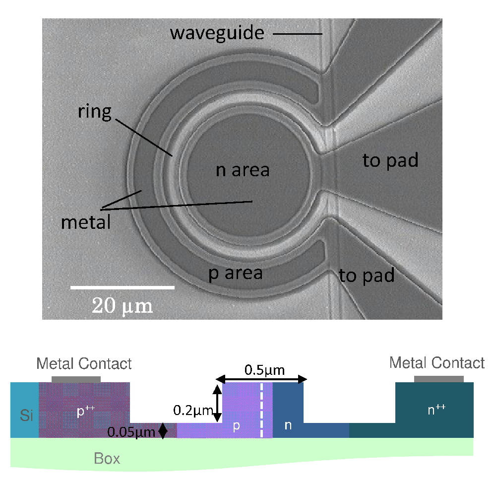 An image of the modulator and a cross-section diagram of the ring waveguide. Source: Kotura
Why is it important?
Optical components use a range of specialist, expensive materials. Silicon is one material that could transform the economics for optics. But for this to happen, the main optical functions – light generation, transmission and detection – need to be supported in silicon. To date, all the required functions except the laser itself - waveguides, modulators and photo-detectors - have been mastered and implemented in silicon.
However, the use of silicon photonics in commercial products has till now been limited. For example, Luxtera makes active optical cable that uses silicon photonics-based transceivers while Kotura has been producing silicon photonics-based VOAs for several years. Its VOA is used within reconfigurable optical add/drop multiplexers (ROADMs) and as a dimmer switch to protect optical receivers from network transients.
Kotura is also supplying its silicon-based Echelle gratings product for 40 and 100 Gigabit Ethernet (GbE) transceiver designs that require the multiplexing and demultiplexing of 4 and 10 wavelengths. The company’s gratings are also being used in Santur’s 100Gbit/s (10x10Gbit/s) transceiver design.
Kotura is in volume production of its VOAs and sampling its Ethernet gratings products, says Arlon Martin, vice-president of marketing and sales at Kotura: “The biggest interest is in 40 Gigabit Ethernet.” Given the small size of the gratings, Kotura is also seeing interest from vendors developing 40GbE transceivers in smaller form factors than the CFP module, such as the QSFP.
This will enable 1Tbit/s data rates over a single fibre to connect high-speed multi-core processor computing elements.
Arlon Martin of Kotura.
But the true potential for silicon photonics, one that promises huge volumes, is very short reach optical interconnects for use in high performance computing and within data centres. Having a low power silicon modulator means it can be integrated with other circuitry in CMOS rather than as a discrete design. Such an integrated approach ensures interconnect reliability.
Method used
There are several ways to modulate a laser. Direct modulation uses electronics to switch the laser on and off at the required rate to imprint the data onto the light. An electro-absorption modulated laser, in contrast, adds an element in front of an always-on laser that either passes or absorbs the light. Kotura’s modulator uses a third approach based on a micro-ring resonator and an adjacent waveguide.
The dimension of the ring – its circumference – dictates when optical resonance occurs. And by carefully matching the power coupling of the micro-ring and waveguide to that of the ring loss, signal attenuation– the light-off condition – is improved. The wavelength at which resonance occurs can be changed by playing with the optical properties of the ring waveguide.
Kotura and Sun have demonstrated the silicon modulator working at up to 11GHz, requiring a peak-to-peak voltage of 2V only. The modulator’s insertion loss is also an attractive 2dB though its working spectrum width is only 0.1nm.
“Our power number – 0.5mW at 10GHz - does not include the driver. But if you want to integrate a number of these on one chip, the low power consumption would enable this,” says Martin. Kotura claims the power consumption achieved is the lowest yet reported.
What next?
The modulator is one of the milestones of the DARPA UNIC programme now into the second of its five-year duration. “This [modulator] is prototype work, not a product,” says Martin, adding that Kotura has not fixed a date as to when the modulator will be commercially used.
As for how the device will ultimately be used, Kotura talks of interfaces operating between 100Gbit/s and 1 Tbit/s. Kotura is already working on an independent programme with CyOptics - the NIST Advanced Technology Programme - developing up to 1Tbit/s links using wavelength division multiplexing (WDM). Such designs use separate laser arrays - each laser at a specific wavelength – as well as gratings and photo-detectors.
In the future inexpensive light sources could generate up to 80 separate modulated lightpaths, Martin says. This will enable 1Tbit/s data rates over a single fibre to connect high-speed multi-core processor computing elements.
Is the idea similar to a broadband light source as proposed for WDM-PON? The UNIC partners have yet to reveal the programme’s detail. “Potentially on the right path,” is all Martin would say.
References:
[1] “Low Vpp, ultralow-energy, compact, high-speed silicon electro-optic modulator.” To read Kotura’s technical paper, click here.
[2] "PHOTONICS APPLIED: INTEGRATED PHOTONICS: Can optical integration solve the computational bottleneck?" OptoIQ, March 1, 2009, click here.