
Q&A with Jerry Rawls - Part 2
The concluding part of the interview with Finisar's executive chairman and company co-founder, Jerry Rawls, to mark the company's 25th anniversary.
Second and final part

Guys that are in the silicon photonics industry have a religion. It does not make any difference what the real economics are, what the real performance is, they talk with a religious fervour about what might be possible with silicon
Q: Over 25 years, what has been one of your better decisions?
Jerry Rawls: After the crash of 2001, we asked what are we going to do in the optics business? Are we going to stay in it? Is there a bright future? And if so, how are we going to respond to it?
We still believed that this was an attractive market and we had built an important brand. And, we knew we could make it more successful in the future, but we were going to have to change the way we did business.
Deciding to become vertically integrated was the key change. At that time, every other company was trying to sell their assets and remove their fixed costs. They were outsourcing manufacturing instead of bringing it in-house. Everyone wanted a variable cost business model, not a fixed cost model. We clearly went against the mainstream.
That is one of the better decisions we ever made.
Equally, with the benefit of hindsight, what do you regret?
A couple of acquisitions that we made in our early years turned out less than desirable. We were sold some technology for which we believed the probability of success was high. We bought the companies based on their technology, not necessarily on their business, and it did not pan out. One thing we learned from those experiences is that when we buy a company, we try to be much more careful about our due diligence.
Another one I regret, although I don't think it was a bad decision: We had created a division in the company called Network Tools that was the leading company in the SAN (storage area network) industry for protocol analysis.
Every company in the world that was creating SAN equipment bought our protocol analysers for Fibre Channel. That was about a $40 million-a-year business and nicely profitable. We sold it [to JDSU] in 2009 and I regret that because we started that business from scratch. It really helped create the SAN industry; it helped our customers prove their equipment interoperability.
We sold it because we had that $250 million in debt we had to pay off. We had borrowed the money and it was now due. It [2009] was still not a great time, we were trying to raise cash and one asset that had value was this division.

How would you describe the current state of the optical component industry and the main challenges it faces?
The optical component industry is in a pretty healthy place. For the most part, the larger companies are doing quite well. Our business is doing nicely. We have had four quarters in a row where revenues have grown, our profitability metrics are improving and our outlook is good. A lot of that has to do with our focus on the data centre market.
We anticipate increasing dollars spent worldwide by phone companies over the next five years
The speeds and feeds in data centres are increasing dramatically: data centres are becoming larger, the connections are faster - connections that used to be copper back in the days of Gigabit Ethernet are now at 10 Gigabits and mostly optical. That transformation of copper to optics that took place in the telephone world 35 years ago is now in full bloom in the data centres. So it is a great time to be in optics because the trends are rolling our way.
We are anticipating spending growth in the telecommunications world with an upgrade in global networks to deal with growing Internet traffic. These networks are changing to very sophisticated ROADM [reconfigurable optical add/drop multiplexer] architectures and 100 Gigabit transmission rates.
We anticipate increasing dollars spent worldwide by phone companies over the next five years. So that sector is going to become healthier and hopefully a larger percentage of our business.
I believe the optical component industry has a number of market opportunities that are going to keep it pretty healthy for some time.
It does not mean that we don't have challenges. The industry, and in particular telecommunications, is fragmented. There are a number of competitors that have very small market share. Many of these competitors are focussing their R&D efforts on the same products - the next generation of telecom equipment - and that is very inefficient. That is the main challenge that the optical industry has, that this fragmentation leads to inefficiency.
That limits the margins of the companies and the industry. It also means that pricing in the industry is at a lower level than component suppliers would like to see.
How that works out is not clear. You could say that in a fragmented industry, you would like to see more consolidation. There will be a little of that. But there are some parts of the industry where consolidation will be very slow.
For example, all of the Japanese optical suppliers are likely to stay in business for some time. Almost every big Japanese electronics company has an optical division, and they always have. None went out of business in the crash of '01 and none went out in the crash of '08 – ’09. That is because these optics divisions are small parts of giant conglomerates. This fragmentation problem is difficult to solve.
Datacom and the data centre appear to be a more interesting segment in terms of driving change than telecom. How do you view the two segments going forward?
I think both are interesting.
The data centre is interesting because of the increased density of Gigabits-per-square-inch on the faceplates of equipment, whether it is switches, storage or servers. Then there is the faster connection speeds between devices and the demand for low latency. The physical size of some of these data centres is demanding that certain connections become single mode - more like wiring a campus as opposed to multi-mode historically used in single buildings.
The datacom market is also very interesting because of a number of connections changing from copper to optical as speeds get faster. Copper transmission demands too much power through big cables at these higher speeds.
In telecom, today what is really exciting is the advent of coherent transmission systems, in particular at 100 Gigabits moving to 400 Gigabit and 1 Terabit-per-second in the next decade.
Coherent transmission is revolutionary in that by using electronics rather than optics to do signal correction for long distance fibre transmission, these signals can be much more efficient, run faster and be much less costly than they have ever been in the past.
Coupled with that is the automation of these optical networks through the extensive use of sophisticated ROADMs. With the next generation of networks, truck rolls to do provisioning and reconfigurations will be almost eliminated.
So there is a lot of excitement for us just because of what is coming to telecom networks. We have been through a lull for the last couple of years but it is a cyclical industry that tends to follow technology waves. We are entering the 100 Gigabit transmission wave and the sophisticated use of many, many ROADMs in these networks for automation.
We have designed silicon photonic chips here at Finisar and have evaluations that are ongoing
Silicon photonics is spoken of as a disruptive technology for datacom and telecom. It also promises to disrupt the component supply chain. What is Finisar's take on the technology?
As a company, we are very product focussed and we want to deliver transmission products and switching products, etc. that fulfill our customers' needs. We don't really care what the technology is. We are going to invest in technology that enables us to build the highest performing and most efficient devices that we can.
Silicon photonics is an interesting technology. We haven't used it in any of our products so far with the exception of a silicon waveguide in an integrated receiver. The most interesting thing about silicon photonics is not just to be able to make waveguides for multiplexers or demultiplexers, but to make modulators.
People have been speculating for years that we will have to use external modulators to achieve higher transmission speeds as we won’t be able to directly drive a laser fast enough.
We make VCSELs by the tens of millions. When we were making them at one Gigabit-per-second [Gbps], there were those in the industry that predicted that we would never be able to run at 2 Gbps as it would be impossible to modulate the lasers that fast. Then we did 2 Gbps, and then there were those that said it would be impossible to do 4, 8 or 10 Gigabits. Well, we are shipping devices today that are 25Gbps VCSELs that are directly modulated.
At every one of those steps there were people investing in silicon photonics companies because they could build modulators they thought would run that fast. I believe every one of those silicon photonics companies went broke.
We now have a new wave of silicon photonics companies. And because Cisco Systems happened to buy one [LightWire], there has been a lot of excitement about silicon photonics.
Well, the physics are such that it is always more efficient to directly modulate a laser - that is, to drive it with an injection of current - than it is to have a continuous wave laser where you externally modulate the light. The external modulation takes more power, more components and more cost.
Guys that are in the silicon photonics industry have a religion. It does not make any difference what the real economics are, what the real performance is, they talk with a religious fervor about what might be possible with silicon.
To date, no one has been able to make light out of silicon. That means one can make a silicon modulator and a silicon waveguide but still have to buy an indium phosphide laser to create light. Then they would have to bond that laser to the silicon substrate in a way that it efficiently launches light, is mechanically stable, and hermetic and that it will stand the rigours of all these networks. That means it can be deployed for 10 or 20 years over temperatures of 0 to 85 degrees C, and survive the qualification torture tests of high humidity, high heat and temperature cycling.
One of the things in the silicon photonics industry to date has been that the packaging - and therefore the yields - have been so difficult, such that the costs have been very high.
I promise you today that for almost every application, silicon photonics costs are higher than using traditional indium phosphide and gallium arsenide lasers and direct modulation.
We don't ignore silicon photonics as a potential technology.
We have designed silicon photonic chips here at Finisar and have evaluations that are ongoing. There are many companies that now offer silicon photonics foundry services. You can lay out a chip and they will build it for you.
We can go to a foundry; we can use their design rules and libraries and design silicon modulators and waveguides and put together a chip with as many splits and Mach-Zehnders that we want. The problem is we haven't found a place where it can be as efficient or offer the performance as using traditional lasers and free-space optics.
Our packaging has been more efficient and our output has been at a higher performance level. Remember that silicon is optically quite lossy. That means you have to launch a lot of light into it to get a little light out.
So far we just haven't found a product where we thought silicon photonics modulation was as efficient as we could build using some other technology. That is true today.
We may use silicon photonics one of these days. In fact, if we look back five or 10 years ago, when we predicted what we would need to build a 100 Gig transponder, silicon photonics was one of our alternatives, and one of the paths we went down in parallel in completing the design.
As it turns out, traditional optics and micro-optical components exceeded our own expectations.
I compare it to the disc drive industry. Twenty years ago people were predicting the demise of the disc drive industry because of solid state memory. It was thought impossible that disc drives would be around five years hence. Well, the guys in the disc industry learned how to increase the bit density and the resolution of the heads and look at the industry today. You can buy a Terabyte drive for less than a hundred dollars. The amazing technology advances they have made have kept them in the game.
What are the biggest challenges facing Finisar?
The biggest challenge we face is meeting the changes in the industry. The use of information is becoming so pervasive - video everywhere and 4G networks - that means all the kids are going to be streaming HD video to some device in their hand. And there is going to be billions of them.
Also, another challenge is managing the expectations of our customers - the equipment companies - in terms of delivering the speeds, densities and the low power performance needed to provide all this information.
It is a daunting task.
We have customers today trying to design systems that will have Terabit-per-second optical links. We don't know how we are going to get there yet but I promise you we will.
The industry in 25 years' time: Still datacom & telecom or something else by then?
In 25 years' time, datacom and telecom will be much more converged.
The data center today is becoming more like wiring a campus network than it is wiring a building as the distances become larger and the speeds faster. Today in data centers we only use point-to-point connections; we use no multiple wavelengths on fibres.
In the telephone world, everything is WDM. Today we are using mostly 96 wavelengths on a single fibre. Those 96 channels can all run at 100 Gbps – a total of nearly 10 Terabit on a single fiber. In the data center world most connections are single wavelengths, point-to-point. But in 25 years, the data centers are going to be using many of the techniques that are used in the telecom networks today in terms of making efficient use of fibres, using multiple colors of light, and being able to switch those individual colours.
For the first part, click here
Terabit interconnect to take hold in the data centre
Intel and Corning have further detailed their 1.6 Terabit interface technology for the data centre.
The collaboration combines Intel's silicon photonics technology operating at 25 Gigabit-per-fibre with Corning's ClearCurve LX multimode fibre and latest MXC connector.
 Silicon photonics wafer and the ClearCurve fibres. Source: Intel
The fibre has a 300m reach, triple the reach of existing multi-mode fibre at such speeds, and uses a 1310nm wavelength. Used with the MXC connector that supports 64 fibres, the overall capacity will be 1.6 Terabits-per-second (Tbps).
"Each channel has a send and a receive fibre which are full duplex," says Victor Krutul, director business development and marketing for silicon photonics at Intel. "You can send 0.8Tbps on one direction and 0.8Tbps in the other direction at the same time."
The link supports connections within a rack and between racks; for example, connecting a data centre's top-of-rack Ethernet switch with an end-of-row one.
James Kisner, an analyst at global investment banking firm, Jefferies, views Intel’s efforts as providing important validation for the fledgling silicon photonics market.
However, in a research note, he points out that it is unclear whether large data centre equipment buyers will be eager to adopt the multi-mode fibre solution as it is more expensive than single mode. Equally, large data centres have increasingly longer span requirements - 500m to 2km - further promoting the long term use of single mode fibre.
Rack Scale Architecture
The latest details of the silicon photonics/ ClearCurve cabling were given as part of an Intel update on several data centre technologies including its Atom C2000 processor family for microservers, the FM5224 72-port Ethernet switch chip, and Intel's Rack Scale Architecture (RSA) that uses the new cabling and connector.
Intel is a member of Facebook's Open Compute Project based on a disaggregated system design that separates storage, computing and networking. "When I upgrade the microprocessors on the motherboard, I don't have to throw away the NICs [network interface controllers] and disc drives," says Krutul. The disaggregation can be within a rack or between rows of equipment. Intel's RSA is a disaggregated design example.
The chip company discussed an RSA design for Facebook. The rack has three 100Gbps silicon photonics modules per tray. Each module has four transmit and four receive fibres, or 24 fibres per tray and per cable. “Different versions of RSA will have more or less modules depending on requirements," says Krutul. Intel has also demonstrated a 32-fibre MXC prototype connector.
Corning says the ClearCurve fibre delivers several benefits. The fibre has a smaller bend radius of 7.5mm, enabling fibre routing on a line card. The 50 micron multimode fibre face is also expanded to 180 microns using a beam expander lens. The lenses make connector alignment easier and less sensitive to dust. Corning says the MXC connector comprises seven parts, fewer than other optical connectors.
Fibre and connector standardisation are key to ensure broad use, says Daryl Inniss, vice president and practice leader, components at Ovum.
"Intel is the only 1310nm multimode transmitter and receiver supplier, and expanding this optical link into other applications like enterprise data centres may require a broader supply base," says Inniss in a comment piece. But the fact that Corning is participating in the development signals a big market in the making, he says.
Intel has not said when the silicon photonics transceiver and fibre/ connector will be generally available. "We are not discussing schedules or pricing at this time," says Krutul.
Silicon photonics: Intel's first lab venture
The chip company has been developing silicon photonics technology for a decade.
"As our microprocessors get faster, you need bigger and faster pipes in and around the servers," says Krutul. "That is a our whole goal - feeding our microprocessors."
Intel is setting up what it calls 'lab ventures', with silicon photonics chosen to be the first.
"You have a research organisation that does not do productisation, and business units that just do products," says Krutul. "You need something in between so that technology can move from pure research to product; a lab venture is an organisational structure to allow that movement to happen."
The lab ventures will be discussed more in the coming year.
Bell Labs on silicon photonics
Briefing: Silicon Photonics
Part 2: A system vendor's perspective
- Silicon photonics as a technology has its challenges
- Its biggest impact could be to shake up the industry's optical component supply chain
- Silicon photonics will not displace VCSELs

An interview with Alcatel-Lucent Bell Labs' Martin Zirngibl, domain leader for enabling physical technologies, on the merits and potential impact of silicon photonics
Martin Zirngibl admits he is skeptical when it comes to silicon photonics. "There is a lot of hype around silicon photonics but there are also some real advantages," he says. "We have a strong silicon photonics programme inside Bell Labs and I tell my folks: If you prove me wrong, I'm going to be very happy."
The skepticism stems from the technology's limitations. "There is no Moore's Law in photonics, you cannot cascade many photonic elements," says Zirngibl.
Photonic components are also analogue. Once several devices are cascaded, the signal loss accumulates. This is true for photonic integration in general, not just silicon photonics.
Another issue is that the size of an optical component such as a laser or a modulator is dictated by the laws of physics rather than lithography, used to make ever-smaller transistors with each generation of CMOS process. Zirngibl compares optical transmitters and receivers to cars: they improve with time but the fundamental size does not change.
"Silicon photonics could form an ASIC-like model and break the supply chain"
A consequence of shrinking feature size with semiconductors is that chip performance gets better with integration. Integration in photonics, in contrast, involves compromise and a tradeoff in optical performance.
However, the advantages of silicon photonics are significant. The technology can benefit from the huge investment made in the semiconductor industry. "CMOS foundries exists with 8- and 12-inch wafers," says Zirngibl. These mature processes are extremely well controlled, producing high-yielding devices. "If you match any component with that type of process, you have instant high volume and instant scalability," says Zirngibl.
Silicon photonics may require something different but if it can use these CMOS processes, the result is a free ride on all this investment, he says: "That is the real advantage.”
For Zirngibl, the impact of silicon photonics will more likely be on the industry supply chain. An optical component maker may sell its device to a packaging company that puts it in a transmitter or receiver optical sub-assembly (TOSA/ROSA). In turn, the sub-assemblies are sold to a module company which then sell the optical transceiver to an equipment vendor. Each player in the supply chain adds its own profit.
Silicon photonics promises to break the model. A system company can design its own chip and go to a silicon foundry. It could then go to a packaging company to make the module or package the device directly on a card, bypassing the module maker altogether.
"Silicon photonics could form an ASIC-like model and break the supply chain," says Zirngibl. "This worries the large module makers of the world."
"The problem with coherent is that it needs a lot of optical stuff"
Zirngibl stresses that such a change could also happen with traditional optical components. A system vendor could adopt a similar strategy with indium phosphide chips, for example. But the issue is that indium phosphide does not share the mature processes or the scale of the semiconductor industry, and as such an ASIC model is harder to achieve.
"If you can use CMOS processes for optical components then, all of a sudden, optical could become an ASIC-like supply chain," says Zirngibl. "It could cut out a lot of the module and package vendors."
That is what Cisco Systems has done with its CPAK module based on silicon photonics. "Cisco broke the supply chain model by doing an internal development of a module, they don't rely on anyone else," he says.
Challenges
Silicon photonics faces several challenges. One is silicon has no optical source. “A regular CMOS process will not product a light source." Companies are pursuing several approaches as to how best to couple a III-V source to silicon.
Another issue is that the optical performance of a silicon photonics design must match that of alternative solutions. "At the end of the day in photonics it is always about performance," says Zirngibl.
A 1dB or 2dB worse insertion loss compared with an alternative photonic design may be acceptable but it has to roughly match. "If it does not, even if the device is for free, the fact that you have a performance degradation will make you pay somewhere else [in the system]," says Zirngibl.
"We once tried access; there is nothing more cost-sensitive than fibre-to-the-home (FTTH) and we wanted to push silicon photonics for access," says Zirngibl. FTTH is highly cost-sensitive and is a volume market. But the resulting design had a 5dB worse performance than a free space equivalent. "We didn't have the slightest chance to get in: a 5dB insertion loss in access means a split ratio of 1:16 instead of 1:32 and a 3-4km reach instead of 20km."
One application where optical performance is key is long-distance transmission using coherent technology. Coherent offers significant benefits: 100 Gigabit per channel, reaches of several thousand kilometers, spectral efficiency, and the ability to correct in the digital domain for many of the transmission impairments.
"The problem with coherent is that it needs a lot of optical stuff," says Zirngibl. A coherent line card has a high power consumption and uses lot of expensive optical components. Companies are looking at silicon photonics as a way of reducing cost while shrinking the size to fit within a pluggable transceiver. The tradeoff is reach; instead of a span of 1000km-plus, achieving a few hundred kilometers would be more likely.
"For interconnect, VCSELs are not going to be displaced"
Companies such as Oclaro, and Finisar and u2t Photonics have announced developments involving indium phosphide to achieve a compact-enough design to fit within a CFP2 pluggable module.
"Silicon photonics has a modulator that can be driven with a low voltage, and that could be driven using CMOS, a real advantage," says Zirngibl. "Unfortunately, the modulator has a lot of insertion loss, so you have to solve it elsewhere."
At OFC/NFOEC 2013, Alcatel-Lucent, working with the CEA-Leti foundry, presented a long-distance laser design using silicon photonics. "We do wafer bonding on silicon - you marry indium phoshide with silicon photonics," says Zirngibl. "If you match a process that allows you to do a light source with 8-inch or 12-inch wafers, you have something that could be a winning solution."
Short-reach connections
One important question that impacts the potential silicon photonics opportunity is when does the crossover from electrical to optical occur?
If the link distance is sufficiently short, it makes sense to stay in the electrical domain. This is because going optical inevitable requires electrical-optical and optical-electrical conversions over a link. "If it is very short distance, it will always be electrical,” says Zirngibl. The issue with electrical is that as signal speeds increase to 25 Gig, losses accumulate very quickly with distance and the signal fades.
"We believe that this crossover from electrical to optical is 1 meter at 100Gbps," says Zirngibl, with the 100 Gigabit being four 25Gbps lanes.
Accordingly, for any distance above 1m, optical interconnect will be used for 100 Gig signals between boards and between systems. “The electrical I/O goes to the end of board where you have a VCSEL interconnect and goes to the next line card, where there is another VCSEL interconnect," says Zirngibl.
In such a design, getting the optics closer to the processor makes sense. "A good case for a processor with almost an optical I/O," says Zirngibl. Companies such as Arista Networks and Compass-EOS are already doing this. "The problem is that it is pretty ugly, cables coming out of the processor, and how do you slide in and out a card?" he says. "What would be really cool is a VCSEL and printed optical waveguides."
This is an area that still needs some work, he says, but there are companies developing optical PCBs such as Vario-optics.
Zirngibl believes one promising application for silicon photonics is for a coherent receiver at 100 Gig. "That is when you will see it [silicon photonics] first," he says. "There is demultiplexing, no light source is needed and you can do the detection on silicon photonics."
For short-reach interconnect, Zirngibl believes silicon photonics will not displace VCSELs.
"VCSELs are by nature an incredibly efficient, low-cost solution," he concludes. "For interconnect, VCSELs are not going to be displaced."
Part 1: Optical interconnect, click here
Part 3: Is silicon photonics an industry game-changer? click here
Arista Networks embeds optics to boost 100 Gig port density
Arista Networks' latest 7500E switch is designed to improve the economics of building large-scale cloud networks.
The platform packs 30 Terabit-per-second (Tbps) of switching capacity in an 11 rack unit (RU) chassis, the same chassis as Arista's existing 7500 switch that, when launched in 2010, was described as capable of supporting several generations of switch design.

"The CFP2 is becoming available such that by the end of this year there might be supply for board vendors to think about releasing them in 2014. That is too far off."
Martin Hull, Arista Networks
The 7500E features new switch fabric and line cards. One of the line cards uses board-mounted optics instead of pluggable transceivers. Each of the line card's ports is 'triple speed', supporting 10, 40 or 100 Gigabit Ethernet (GbE). The 7500E platform can be configured with up to 1,152 10GbE, 288 40GbE or 96 100GbE interfaces.
The switch's Extensible Operating System (EOS) also plays a key role in enabling cloud networks. "The EOS software, run on all Arista's switches, enables customers to build, manage, provision and automate these large scale cloud networks," says Martin Hull, senior product manager at Arista Networks.
Applications
Arista, founded in 2004 and launched in 2008, has established itself as a leading switch player for the high-frequency trading market. Yet this is one market that its latest core switch is not being aimed at.
"With the exception of high-frequency trading, the 7500 is applicable to all data centre markets," says Hull. "That it not to say it couldn't be applicable to high-frequency trading but what you generally find is that their networks are not large, and are focussed purely on speed of execution of their transactions." Latency is a key networking performance parameter for trading.
The 7500E is being aimed at Web 2.0 companies and cloud service providers. The Web 2.0 players include large social networking and on-line search companies. Such players have huge data centres with up to 100,000 servers.
The same network architecture can also be scaled down to meet the requirements of large 'Fortune 500' enterprises. "Such companies are being challenged to deliver private cloud as the same competitive price points as the public cloud," says Hull.
The 7500 switches are typically used in a two-tier architecture. For the largest networks, 16 or 32 switches are used on the same switching tier in an arrangement known as a parallel spine.
A common switch architecture for traditional IT applications such as e-mail and e-commerce uses three tiers of switching. These include core switches linked to distribution switches, typically a pair of switches used in a given area, and top-of-rack or access switches connected to each distribution pair.
For newer data centre applications such as social networking, cloud services and search, the computation requirements result in far greater traffic shared on the same tier of switching, referred to as east-west traffic. "What has happened is that the single pair of distribution switches no longer has the capacity to handle all of the traffic in that distribution area," says Hull.
Customers address east-west traffic by throwing more platforms together. Eight or 16 distribution switches are used instead of a pair. "Every access switch is now connected to each one of those 16 distribution switches - we call them spine switches," says Hull.
The resulting two-tier design, comprising access switches and distribution switches, requires that each access switch has significant bandwidth between itself and any other access switch. As a result, many 7500 switches - 16 or 32 - can be used in parallel at the distribution layer.
 Source: Arista Networks
"If I'm a Fortune 500 company, however, I don't need 16 of those switches," says Hull. "I can scale down, where four or maybe two [switches] are enough." Arista also offers a smaller 4-slot chassis as well as the 8 slot (11 RU) 7500E platform.
7500E specification
The switch has a capacity of 30Tbps. When the switch is fully configured with 1,152 10GbE ports, it equates to 23Tbps of duplex traffic. The system is designed with redundancy in place.
"We have six fabric cards in each chassis," says Hull, "If I lose one, I still have 25 Terabits [of switching fabric]; enough forwarding capacity to support the full line rates on all those ports." Redundancy also applies to the system's four power supplies. Supplies can fail and the switch will continue to work, says Hull.
The switch can process 14.4 billion 64-byte packets a second. This, says Hull, is another way of stating the switch capacity while confirming it is non-blocking.
The 7500E comes with four line card options: three use pluggable optics while the fourth uses embedded optics, as mentioned, based on 12 10Gbps transmit and 12 10Gbps receive channels (see table).

Using line cards supporting pluggable optics provides the customer the flexibility of using transceivers with various reach options, based on requirements. "But at 100 Gigabit, the limiting factor for customers is the size of the pluggable module," says Hull.
Using a CFP optical module, each card supports four 100Gbps ports only. The newer CFP2 modules will double the number to eight. "The CFP2 is becoming available such that by the end of this year there might be supply for board vendors to think about releasing them in 2014," says Hull. "That is too far off."
Arista's board mounted optics delivers 12 100GbE ports per line card.
The board-mounted triple-speed ports adhere to the IEEE 100 Gigabit SR10 standard, with a reach of 150m over OM4 fibre. The channels can be used discretely for 10GbE, grouped in four for 40GbE, while at 100GbE they are combined as a set of 10.
"At 100 Gig, the IEEE spec uses 20 out of 24 lanes (10 transmit and 10 receive); we are using all 24," says Hull. "We can do 12 10GbE, we can do three 40GbE, but we can still only do one 100Gbps because we have a little bit left over but not enough to make another whole 100GbE." In turn, the module can be configured as two 40GbE and four 10GbE ports, or 40GbE and eight 10GbE.
Using board-mounted optics reduces the cost of 100Gbps line card ports. A full 96 100GbE switch configuration achieves a cost of $10k/port while using existing CFP modules the cost is $30k-50k/ port, claims Arista.
Arista quotes 10GbE as costing $550 per line card port not including the pluggable transceiver. At 40GbE this scales to $2,200. For 100GbE the $10k/ port comprises the scaled-up port cost at 100GbE ($2.2k x 2.5) to which is added the cost of the optics. The power consumption is under 4W/ port when the system is fully loaded.
The company uses merchant chips rather than an in-house ASIC for its switch platform. Can't other vendors develop similar performance systems based on the same ICs? "They could, but it is not easy," says Hull.
The company points out that merchant chip switch vendors use a CMOS process node that is typically a generation ahead of state-of-the-art ASICs. "We have high-performance forwarding engines, six per line card, each a discrete system-on-chip solution," says Hull. "These have the technology to do all the Layer 2 and Layer 3 processing." All these devices on one board talk to all the other chips on the other cards through the fabric.
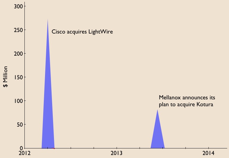
In the last year, equipment makers have decided to bring silicon photonics technology in-house: Cisco Systems has acquired Lightwire while Mellanox Technologies has announced its plan to acquire Kotura.
Arista says it is watching silicon photonics developments with keen interest. "Silicon photonics is very interesting and we are following that," says Hull. "You will see over the next few years that silicon photonics will enable us to continue to add density."
There is a limit to where existing photonics will go, and silicon photonics overcomes some of those limitations, he says.
Extensible Operating System
Arista's highlights several characteristics of its switch operating system. The EOS is standards-compliant, self-healing, and supports network virtualisation and software-defined networking (SDN).
The operating system implements such protocols as Border Gateway Protocol (BGP) and spanning tree. "We don't have proprietary protocols," says Hull. "We support VXLAN [Virtual Extensible LAN] an open standards way of doing Layer 2 overlay of [Layer] 3."
EOS is also described as self-healing. The modular operating system is composed of multiple software processes, each process described as an agent. "If you are running a software process and it is killed because it is misbehaving, when it comes back typically its work is lost," says Hull. EOS is self-healing in that should an agent need to be restarted, it can continue with its previous data.
"We have software logic in the system that monitors all the agents to make sure none are misbehaving," says Hull. "If it finds an agent doing stuff that it should not, it stops it, restarts it and the process comes back running with the same data." The data is not packet related, says Hull, rather the state of the network.
The operating system also supports network virtualisation, one aspect being VXLAN. VXLAN is one of the technologies that allows cloud providers to provide a customer with server resources over a logical network when the server hardware can be distributed over several physical networks, says Hull. "Even a VLAN can be considered as network virtualisation but VXLAN is the most topical."
Support for SDN is an inherent part of EOS from its inception, says Hull. “EOS is open - the customers can write scripts, they can write their own C-code, or they can install Linux packages; all can run on our switches." These agents can talk back to the customer's management systems. "They are able to automate the interactions between their systems and our switches using extensions to EOS," he says.
"We encompass most aspects of SDN," says Hull. "We will write new features and new extensions but we do not have to re-architect our OS to provide an SDN feature."
Arista is terse about its switch roadmap.
"Any future product would improve performance - capacity, table sizes, price-per-port and density," says Hull. "And there will be innovation in the platform's software.
Mellanox to acquire silicon photonics player Kotura
 Source: Gazettabyte
Mellanox Technologies has announced its intention to acquire silicon photonics player, Kotura, for $82 million.
The acquisition will enable Mellanox to deliver 100 Gigabit Infiniband and Ethernet interconnect in the coming two years. lt will also provide Kotura with the resources needed to bring its 100 Gigabit QSFP to market. Mellanox will also gain Kotura's optical engine for use in active optical cables and new mid-plane platform designs, as well as future higher speed interfaces.
The news is also significant for the optical component industry. Kotura is one of the three established merchant silicon photonics players - the others being LightWire and Luxtera - that have spent years developing their technologies.
LightWire was acquired by Cisco Systems in March 2012 for US $271 million and now Mellanox plans to acquire Kotura. The two equipment vendors recognise the value of the technology, bringing it in-house to reduce system interconnect costs and as a long term differentiator for their equipment and ASIC designs. Mellanox, as a silicon photonics player, will compete with Intel, with its own silicon photonics technology, and Cisco Systems.
Kotura has been using its technology to sell telecom products such as variable optical attenuators and multiplexers. The start-up recently announced its 100 Gig QSFP that uses wavelength division multiplexing (WDM) transmitter and receiver chips. The product is to become available in 2014.
In an interview last year, Kotura's CTO, Mehdi Asghari, discussed a roadmap showing how its 100 Gigabit silicon photonics technology could scale to 400 Gigabit and eventually 1.6 Terabit.
"Our devices are capable of running at 40 or 50 Gigabit-per-second (Gbps), depending on the electronics. The electronics is going to limit the speed of our devices. We can very easily see going from four channels at 25Gbps to 16 channels at 25Gbps to provide a 400 Gigabit solution," Asghari told Gazettabyte.
Kotura also discussed how the line rate could be increased to 50Gbps either using a non-return-to-zero (NRZ) line rate or using a multi-level modulation such as pulse amplitude modulation (PAM).
"To get to 1.6 Terabit transceivers, we envisage something running at 40Gbps times 40 channels or 50Gbps times 32 channels. We already have done a single receiver chip demonstrator that has 40 channels, each at 40Gbps," said Asghari.
"These things in silicon are not a big deal. The III-V guys really struggle with yield and cost. But you can envisage scaling to that level of complexity in a silicon platform."
Silicon photonics will not replace existing VCSEL or indium phosphide-based transceiver designs. But there is no doubting silicon photonics is emerging as a key optical technology and the segment is heating up.
If the early start-ups are being acquired, there have been more recent silicon photonics players entering the marketplace such as Aurrion, Skorpios Technologies and Teraxion. There are also internal developments among equipment players such as Alcatel-Lucent, HP Labs and IBM. Indeed Kotura has worked closely with Oracle (Sun Microsystems)
Further acquisitions of silicon photonic players should be expected as companies start designing next generation, denser systems and adopt 100 Gigabit and faster interfaces.
Equally, established optical component and module companies will likely enter quietly (and not so quietly) the marketplace adding silicon photonics to their technology toolkits when the timing is right.
Trends to watch
Two industry trends are underway regarding silicon photonics.
The first is system vendors wanting to own the technology to reduce their costs while recognising a need to control and understand the technology as they tackle more complex equipment designs.
The other, what at first glance is a contrarian trend, is the democratisation of silicon photonics.
The technology is slowly passing from the select few to become more generally available for industry use. For this to happen, the relevant design tools need to mature as do third-party fabrication plants that will manufacture the silicon photonics designs.
Appendix:
On June 4th, 2013, Mellanox announced a definitive agreement to acquire chip company IPtronics for $47.5 million as it builds out its in-house technologies for optical interconnect. Click here
Futher reading:
Avago to acquire CyOptics, click here
OFC/NFOEC 2013 industry reflections - Final part
Gazettabyte spoke with Jörg-Peter Elbers, vice president, advanced technology at ADVA Optical Networking about the state of the optical industry following the recent OFC/NFOEC exhibition.
"There were many people in the OFC workshops talking about getting rid of pluggability and the cages and getting the stuff mounted on the printed circuit board instead, as a cheaper, more scalable approach"
Jörg-Peter Elbers, ADVA Optical Networking
Q: What was noteworthy at the show?
A: There were three big themes and a couple of additional ones that were evolutionary. The headlines I heard most were software-defined networking (SDN), Network Functions Virtualisation (NFV) and silicon photonics.
Other themes include what needs to be done for next-generation data centres to drive greater capacity interconnect and switching, and how do we go beyond 100 Gig and whether flexible grid is required or not?
The consensus is that flex grid is needed if we want to go to 400 Gig and one Terabit. Flex grid gives us the capability to form bigger pipes and get those chunks of signals through the network. But equally it allows not only one interface to transport 400 Gig or 1 Terabit as one chunk of spectrum, but also the possibility to slice and dice the signal so that it can use holes in the network, similar to what radio does.
With the radio spectrum, you allocate slices to establish a communication link. In optics, you have the optical fibre spectrum and you want to get the capacity between Point A and Point B. You look at the spectrum, where the holes [spectrum gaps] are, and then shape the signal - think of it as software-defined optics - to fit into those holes.
There is a lot of SDN activity. People are thinking about what it means, and there were lots of announcements, experiments and demonstrations.
At the same time as OFC/NFOEC, the Open Networking Foundation agreed to found an optical transport work group to come up with OpenFlow extensions for optical transport connectivity. At the show, people were looking into use cases, the respective technology and what is required to make this happen.
SDN starts at the packet layer but there is value in providing big pipes for bandwidth-on-demand. Clearly with cloud computing and cloud data centres, people are moving from a localised model to a cloud one, and this adds merit to the bandwidth-on-demand scenario.
This is probably the biggest use case for extending SDN into the optical domain through an interface that can be virtualised and shared by multiple tenants.
"This is not the end of III-V photonics. There are many III-V players, vertically integrated, that have shown that they can integrate and get compact, high-quality circuits"
Network Functions Virtualisation: Why was that discussed at OFC?
At first glance, it was not obvious. But looking at it in more detail, much of the infrastructure over which those network functions run is optical.
Just take one Network Functions Virtualisation example: the mobile backhaul space. If you look at LTE/ LTE Advanced, there is clearly a push to put in more fibre and more optical infrastructure.
At the same time, you still have a bandwidth crunch. It is very difficult to have enough bandwidth to the antenna to support all the users and give them the quality of experience they expect.
Putting networking functions such as cacheing at a cell site, deeper within the network, and managing a virtualised session there, is an interesting trend that operators are looking at, and which we, with our partnership with Saguna Networks, have shown a solution for.
Virtualising network functions such as cacheing, firewalling and wide area network (WAN) optimisation are higher layer functions. But as you do that, the network infrastructure needs to adapt dynamically.
You need orchestration that combines the control and the co-ordination of the networking functions. This is more IT infrastructure - server-based blades and open-source software.
Then you have SDN underneath, supporting changes in the traffic flow with reconfiguration of the network infrastructure.
There was much discussion about the CFP2 and Cisco's own silicon photonics-based CPAK. Was this the main silicon photonics story at the show?
There is much interest in silicon photonics not only for short reach optical interconnects but more generally, as an alternative to III-V photonics for integrated optical functions.
For light sources and amplification, you still need indium phosphide and you need to think about how to combine the two. But people have shown that even in the core network you can get decent performance at 100 Gig coherent using silicon photonics.
This is an interesting development because such a solution could potentially lower cost, simplify thermal management, and from a fab access and manufacturing perspective, it could be simpler going to a global foundry.
But a word of caution: there is big hype here too. This is not the end of III-V photonics. There are many III-V players, vertically integrated, that have shown that they can integrate and get compact, high-quality circuits.
You mentioned interconnect in the data centre as one evolving theme. What did you mean?
The capacities inside the data centre are growing much faster than the WAN interconnects. That is not surprising because people are trying to do as much as possible in the data centre because WAN interconnect is expensive.
People are looking increasingly at how to integrate the optics and the server hardware more closely. This is moving beyond the concept of pluggables all the way to mounted optics on the board or even on-chip to achieve more density, less power and less cost.
There were many people in the OFC workshops talking about getting rid of pluggability and the cages and getting the stuff mounted on the printed circuit board instead, as a cheaper, more scalable approach.
"Right now we are running 28 Gig on a single wavelength. Clearly with speeds increasing and with these kind of developments [PAM-8, discrete multi-tone], you see that this is not the end"
What did you learn at the show?
There wasn't anything that was radically new. But there were some significant silicon photonics demonstrations. That was the most exciting part for me although I'm not sure I can discuss the demos [due to confidentiality].
Another area we are interested in revolves around the ongoing IEEE work on short reach 100 Gigabit serial interfaces. The original objective was 2km but they have now honed in on 500m.
PAM-8 - pulse amplitude modulation with eight levels - is one of the proposed solutions; another is discrete multi-tone (DMT). [With DMT] using a set of electrical sub-carriers and doing adaptive bit loading means that even with bandwidth-limited components, you can transmit over the required distances. There was a demo at the exhibition from Fujitsu Labs showing DMT over 2km using a 10 Gig transmitter and receiver.
This is of interest to us as we have a 100 Gigabit direct detection dense WDM solution today and are working on the product evolution.
We use the existing [component/ module] ecosystem for our current direct detect solution. These developments bring up some interesting new thoughts for our next generation.
So you can go beyond 100 Gigabit direct detection?
Right now we are running 28 Gig on a single wavelength. Clearly with speeds increasing and with these kind of developments [PAM-8, DMT], you see that this is not the end.
Part 1: Software-defined networking: A network game-changer, click here
Part 2: OFC/NFOEC 2013 industry reflections, click here
Part 3: OFC/NFOEC 2013 industry reflections, click here
Part 4: OFC/NFOEC industry reflections, click here
Avago to acquire CyOptics
- Avago to become the second largest optical component player
- Company gains laser and photonic integration technologies
- The goal is to grow data centre and enterprise market share
- CyOptics achieved revenues of $210M in 2012
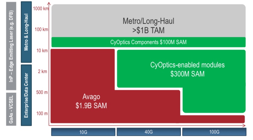 How the acquisition of CyOptics will expand Avago's market opportunities. SAM is the serviceable addressable market and TAM is the total addressable market. Source: Avago
Avago Technologies has announced its plan to acquire optical component player, CyOptics. The value of the acquisition, at US $400M, is double CyOptics' revenues in 2012.
CyOptics' sales were $210M last year, up 21 percent from the previous year. Avago's acquisition will make it the optical component industry's second largest company, behind Finisar, according to market research firm, Ovum. The deal is expected to be completed in the third quarter of the year.
The deal will add indium phosphide and planar lightwave circuit (PLC) technologies to Avago's vertical-cavity surface-emitting laser (VCSEL) and optical transceiver products. In particular, Avago will gain edge laser technology and photonic integration expertise. It will also inherit an advanced automated manufacturing site as well as entry into new markets such as passive optical networking (PON).
Avago stresses its interest in acquiring CyOptics is to bolster its data centre offerings - in particular 40 and 100 Gigabit data centre and enterprise applications - as well as benefit from the growing PON market.
The company has no plans to enter the longer distance optical transmission market beyond supplying optical components.

Significance
Ovum views the acquisition as a shift in strategy. Avago is known as a short distance interconnect supplier based on its VCSEL technology.
"Avago has seen that there are challenges being solely a short-distance supplier, and there are opportunities expanding its portfolio and strategy," says Daryl Inniss, Ovum's vice president and practice leader components.
Such opportunities include larger data centres now being built and their greater use of single-mode fibre that is becoming an attractive alternative to multi-mode as data rates and reach requirements increase.
"Avago's revenues can be lumpy partly because they have a few really large customers," says Inniss.
Another factor motivating the acquisition is that short-distance interconnect is being challenged by silicon photonics. "In the long run silicon photonics is going to win," he says.
What Avago will gain, says Inniss, is one of the best laser suppliers around. And its acquisition will impact adversely other optical module players. "CyOptics is a supplier to several transceiver vendors," says Inniss. "The outlook, two or three years' hence, is decreased business as a merchant supplier."
Inniss points out that CyOptics will represent the second laser manufacturer acquisition this year, following NeoPhotonics's acquisition of Lapis Semiconductor which has 40 Gigabit-per-second (Gbps) electro-absorption modulator lasers (EMLs).
These acquisitions will remove two merchant EML suppliers, given that CyOptics is a strong 10Gbps EML player, and lasers are a key technological asset.
See also:
For a 2011 interview with CyOptics' CEO, click here
OFC/NFOEC 2013 industry reflections - Part 4
Gazettabyte asked industry figures for their views after attending the recent OFC/NFOEC show.
"Spatial domain multiplexing has been a hot topic in R&D labs. However, at this year's OFC we found that incumbent and emerging carriers do not have a near-term need for this technology. Those working on spatial domain multiplexing development should adjust their efforts to align with end-users' needs"
T.J. Xia, Verizon
T.J. Xia, distinguished member of technical staff, Verizon
Software-defined networking (SDN) is an important topic. Looking forward, I expect SDN will involve the transport network so that all layers in the network are controlled by a unified controller to enhance network efficiency and enable application-driven networking.
Spatial domain multiplexing has been a hot topic in R&D labs. However, at this year's OFC we found that incumbent and emerging carriers do not have a near-term need for this technology. Those working on spatial domain multiplexing development should adjust their efforts to align with end-users' needs.
Several things are worthy to watch. Silicon photonics has the potential to drop the cost of optical interfaces dramatically. Low-cost pluggables such as CFP2, CFP4 and QSFP28 will change the cost model of client connections. Also, I expect adaptive, DSP-enabled transmission to enable high spectral efficiencies for all link conditions.
Andrew Schmitt, principal analyst, optical at Infonetics Research
The Cisco CPAK announcement was noteworthy because the amount of attention it generated was wildly out of proportion to the product they presented. They essentially built the CFP2 with slightly better specs.
"It was very disappointing to see how breathless people were about this [CPAK] announcement. When I asked another analyst on a panel if he thought Cisco could out-innovate the entire component industry he said yes, which I think is just ridiculous."
Cisco has successfully exploited the slave labour and capital of the module vendors for over a decade and I don't see why they would suddenly want to be in that business.
The LightWire technology is much better used in other applications than modules, and ultimately the CPAK is most meaningful as a production proof-of-concept. I explored this issue in depth in a research note for clients.
It was very disappointing to see how breathless people were about this announcement. When I asked another analyst on a panel if he thought Cisco could out-innovate the entire component industry he said yes, which I think is just ridiculous.
There were also some indications surrounding CFP2 customers that cast doubt on the near-term adoption of the technology, with suppliers such as Sumitomo Electric deciding to forgo development entirely in favour of CFP4 and/ or QSFP.
I think CFP2 ultimately will be successful outside of enterprise and data centre applications but there is not a near-term catalyst for adoption of this format, particularly now that Cisco has bowed out, at least for now.
SDN is a really big deal for data centres and enterprise networking but its applications in most carrier networks will be constrained to only a few areas relative to multi-layer management.
Within carrier networks, I think SDN is ultimately a catalyst for optical vendors to potentially add value to their systems, and a threat to router vendors as it makes bypass architectures easier to implement.
"Pluggable coherent is going to be just huge at OFC/NFOEC 2014"
Optical companies like ADVA Optical Networking, Ciena and Infinera are pushing the envelope here and the degree to which optical equipment companies are successful is dependent on who their customers are and how hungry these customers are for solutions.
Meanwhile, pluggable coherent is going to be just huge at OFC/NFOEC 2014, followed by QSFP/ CFP4 prototyping and more important production planning and reliability. Everyone is going to use different technologies to get there and it will be interesting to see what works best.
I also think the second half of 2013 will see an increase in deployment of common equipment such as amplifiers and ROADMs.
Magnus Olson, director hardware engineering, Transmode
Two clear trends from the conference, affecting quite different layers of the optical networks, are silicon photonics and SDN.
"If you happen to have an indium phosphide fab, the need for silicon photonics is probably not that urgent. If you don't, now seems very worthwhile to look into silicon photonics"
Silicon photonics, deep down in the physical layer, is now emerging rapidly from basic research to first product realisation. Whereas some module and component companies barely have taken the step from lithium niobate modulators to indium phospide, others have already advanced indium phosphide photonic integrated circuits (PICs) in place.
If you happen to have an indium phosphide fab, the need for silicon photonics is probably not that urgent. If you don't, now seems very worthwhile to look into silicon photonics.
Silicon photonics is a technology that should help take out the cost of optics for 100 Gigabit and beyond, primarily for short distance, data centre applications.
SDN, on the other hand, continues to mature. There is considerable momentum and lively discussion in the research community as well as within the standardisation bodies that could perhaps help SDN to succeed where Generalized Multi-Protocol Label Switching (GMPLS) failed.
Ongoing industry consolidation has reduced the number of companies to meet and discuss issues with to a reasonable number. The larger optical module vendors all have full portfolios and hence the consolidation would likely slow down for awhile. The spirit at the show was quite optimistic, in a very positive, sustainable way.
As for emerging developments, the migration of form factors for 100 Gigabit, from CFP via CFP2 to CFP4 and beyond, is important to monitor and influence from a wavelength-division multiplexing (WDM) vendor point of view.
We should learn from the evolution of the SFP+, originally invented with purely grey data centre applications. Once the form factor is well established and mature, coloured versions start to appear.
If not properly taken into account from the start in the multi-source agreement (MSA) work with respect to, for example, power classes, it is not easy to accommodate tunable dense WDM versions in these form factors. Pluggable optics are crucial for cost as well as flexibility, on both the client side and line side.
Shai Rephaeli, vice president of interconnect products, Mellanox
At OFC, many companies demonstrated 25 Gigabit-per-second (Gbps) prototypes and solutions, both multi mode and single mode.
Thus, a healthy ecosystem for the 100 Gigabit Ethernet (GbE) and EDR (Enhanced Data Rate) InfiniBand looks to be well aligned with our introduction of new NIC (network interface controller)/ HCA (Infiniband host channel adaptor) and switch systems.
However, a significant increase in power consumption compared to current 10Gbps and 14Gbps product is observed. This requires the industry to focus heavily on power optimisation and thermal solutions.
"One development to watch is 1310nm and 1550nm VCSELs"
Standardisation for 25Gbps single mode fibre solutions is a big challenge. All the industry leaders have products at some level of development, but each company is driving its own technology. There may be a real interoperability barrier, considering the different technologies: WDM/ 1310nm, parallel and pulse-amplitude modulation (PAM) which, itself, may have several flavours: 4-levels, 8-levels and 16-levels.
One development to watch is 1310nm and 1550nm VCSELs, which can bring the data centre/ multi-mode fibre volume and prices into the mid-reach market. This technology can be important for the new large-scale data centres, requiring connections significantly longer than 100m.
Part 1: Software-defined networking: A network game-changer, click here
Part 2: OFC/NFOEC 2013 industry reflections, click here
Part 3: OFC/NFOEC 2013 industry reflections, click here
Part 5: OFC/NFEC 2013 industry reflections, click here
OFC/NFOEC 2013 industry reflections - Part 3

Joe Berthold, vice president of network architecture, Ciena
The two topics that received the most attention, judging from session attendance and discussion in the hallways, were silicon photonics and software-defined networking (SDN). I predict that next year those who wish to capitalise on this popularity wave will be submitting papers on SDN-enabled silicon photonics.
More seriously, though, there remains vigorous debate about the relative importance of III-V integrated optics and silicon photonics, and I look forward to seeing how this evolves in the marketplace.
"Some of the SDN-related talks from the global research and education community were very good. They have been pioneers in making high capacity optical networks dynamic, and we have much to learn from them as they have several years experience building and operating SDNs, even before the term existed."
With respect to SDN and service providers, it is going to be several years before we see a true, SDN-enabled network as there are many other issues that need to be addressed.
This is one of the reasons Ciena is taking a lead role in the Open Networking Foundation's investigation of applying OpenFlow or the like at the optical layers. I thought some of the SDN-related talks from the global research and education community were very good. They have been pioneers in making high capacity optical networks dynamic, and we have much to learn from them as they have several years experience building and operating SDNs, even before the term existed.
"One of the most interesting commercial developments to watch in the coming years related to 100 Gig is the work that has begun on pluggable coherent analogue optical modules"
There was also quite a bit of buzz about 100 Gig deployments. It was nice to hear one of the industry analysts refer to 2013 as the year of 100 Gig as this is an area where Ciena has been quite successful.
I did not see or hear of any dramatic advances reported at the conference. What I did see, in talks and on the show floor, was a broad base of technology development that will lead to increased system density and lower cost and power.
On the client side, many companies showed 100 Gig CFP2 modules, and there was quite a bit of talk and demonstrations of technology building blocks that will lead to even smaller size.
Another optical networking topic that means many different things to different people was flexible grids and flexible transmission formats. From speaking with a number of network operators, it seems there is an appreciation for the future-proofing benefit of flexible grid ROADMs, but a recognition that the spectral efficiency gains to be had are quite limited, especially in a ROADM mesh network. So they are emerging as a nice-to-have feature but not a must-have-at-any-price feature.
Another 'flex' concept is flex-transceivers. The flavour of flex-transceivers that seem by most I spoke with to be practical are those that maintain a fixed baud rate but vary modulation format, say from BPSK to QPSK, 8PSK, 16QAM and perhaps beyond, to fit different distance applications.
I think one of the most interesting commercial developments to watch in the coming years related to 100 Gig is the work that has begun on pluggable coherent analogue optical modules, likely to emerge in a CFP2 form factor. I view this as a major next step the industry will take to reduce the cost and increase the density of coherent interfaces on switches and transmission systems.
The OIF did the industry a great service in pulling together a set of interoperable building blocks that form the photonic foundation of 100 Gig solutions today. The next step is to integrate these pieces and place them in a pluggable module. There is yet no formal project with this goal, but discussions are underway.
Watch this space...
Karen Liu, principal analyst components, Ovum.
There was a real sense of openness to new directions even as a lot of short-term activity continues to focus on getting 100 Gig to full maturity. Instead of pitching their favourite directions, some people actually solicited more ideas.
"One trend to watch is the battle between VCSELs and silicon photonics"
Directions that seemed promising but unformed last year got a bit firmed up. Connections are being made from the application down to the device technology. What had been wacky ideas previously are being taken seriously:
- Optical circuit switching looks like it will have a place in conjunction with Ethernet switching.
- Spatial division multiplexing is the hot research topic. I like the work that Bell Labs is doing, particularly where the add/drop increment ties together multiple cores of the same wavelength so compensation algorithms can take advantage of similar environmental history. This is moving past the physics, to thinking about network architecture.
- Monolithic integration of electronics with photonics. Early stages still and primarily around the drivers. But as this is motivated by power consumption, it seems like a solid direction that will have legs.
One trend to watch is the battle between VCSELs (vertical-cavity surface-emitting lasers) and silicon photonics. Conventional wisdom was that VCSELS were for multi-mode and silicon photonics for single-mode but both have crossed over into the other's space.
 Martin Guy, vice-president of product management and technology Teraxion
There were several noteworthy developments. In particular, silicon photonics has started to show its promises as new products are introduced:
- Cisco announced its 100 Gig CPAK transceiver following the Lightwire acquisition
- Kotura showed its 100 Gig WDM QSFP package with only 3.5 W of power consumption.
- Luxtera demonstrated a 100 Gig QSFP package using four fibre pairs, each [fibre] carrying 25Gbps.
- Teraxion introduced its small form factor coherent receiver based on silicon photonics
Silicon photonics was also largely discussed at the technical conference and very impressive results were demonstrated. Most notably, Cisco and Alcatel-Lucent presented results on silicon photonic modulators for metro and long-haul coherent systems with performance comparable to lithium niobate.
Tunable laser technologies on silicon photonics were also presented by companies such as Skorpios and Aurrion during the post-deadline sessions.
"Cisco and Alcatel-Lucent presented results on silicon photonic modulators for metro and long-haul coherent systems with performance comparable to lithium niobate."
All those new silicon photonics technologies could eventually become key building blocks of future highly-integrated transceivers.
Pluggable coherent modules will be a big market opportunity and it is all about density and low power consumption.
At the show, Oclaro demonstrated key milestones to bring to market a CFP2 coherent module by mid-2014 while this product is on the roadmap of all other major transceiver vendors.
From Teraxion’s perspective, our recent acquisition of Cogo Optronics Canada for high-speed modulators is directly in line with this market trend at the modules level where performance, size and low power consumption are key requirements.
Paul Brooks, product line manager for high-speed test solutions, JDSU
The growing confidence in second-generation 100 Gig CFP2s was evident at the show. Many companies, including JDSU, demonstrated robust second-generation 100 Gig modules which will drive confidence across the whole 100 Gig ecosystem to allow cost efficient 100 Gig clients. Our ONT CFP2 test solution was well received and we spent a lot of time demonstrating the features that will enable successful CFP2 deployment.
"Many companies are openly discussing 400 Gig and beyond, the bandwidth demand is there but considerable technology challenges need to be address"
One thing enforced at the show is the continued importance of innovation in test and measurement solutions required by our customers as we move to 100 Gig+ systems.
Many companies are openly discussing 400 Gig and beyond, the bandwidth demand is there but considerable technology challenges need to be address. The intellectual horsepower present at the show allows fruitful and engaging discussions on key topics.
See also:
Part 1: Software-defined networking: A network game-changer, click here
Part 2: OFC/NFOEC industry reflections, click here
Part 4: OFC/NFOEC industry reflections, click here
Part 5: OFC/NFEC 2013 industry reflections, click here
OFC/NFOEC 2013 product round-up - Part 1
Part 1: Client-side transceivers
- First CFP2 single-mode and multi-mode transceiver announcements
- Cisco Systems unveils its CPAK module
- 100 Gigabit QSFPs from Kotura and Luxtera
- CFP2 and 40km CFP 10x10 MSA modules
- Infiniband FDR and 'LR4 superset' QSFPs
The recent OFC/NFOEC exhibition and conference held in Anaheim, California, saw a slew of optical transceiver announcements. The first CFP2 client-side products for single-mode and multi-mode fibre were unveiled by several companies, as was Cisco Systems' in-house CPAK transceiver.
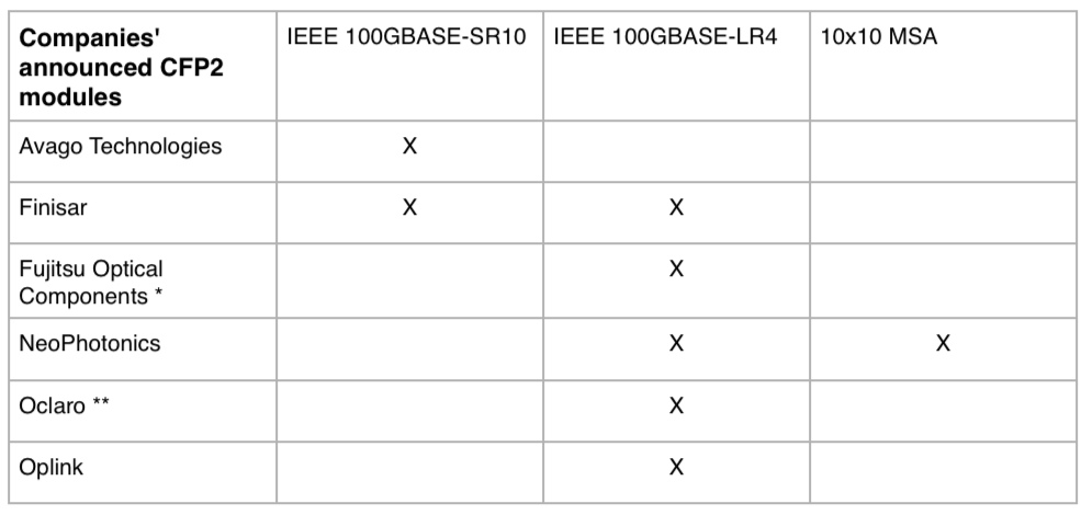
The CFP2 is the pluggable form factor that follows the first generation CFP. The CFP MSA announced the completion of the CFP2 specification at the show, while several vendors including Avago Technologies, Finisar, Fujitsu Optical Components, NeoPhotonics, Oclaro and Oplink Communications detailed their first CFP2 products.
The 40 and 100 Gigabit CFP2 is half the size of the CFP, enabling at least a doubling of the CFP2 transceivers on a faceplate compared to four CFPs (see table below). The CFP2 is also future-proofed to support 200 and 400Gbps (See first comment at bottom of CFP2 story).
Another difference between the CFP and the CFP2 is that the CFP2 uses a 4x25Gbps electrical interface. Accordingly, the CFP2 does not need the 'gearbox' IC that translates between ten, 10 Gigabit-per-second (Gbps) lanes to four, 25Gbps electrical lanes that interface to the 4x25/28Gbps optics. Removing the gearbox IC saves space and reduces the power consumption by several watts.
The industry has long settled on the SFP+ at 10Gbps while the QSFP has become the 40Gbps form factor of choice. With 100Gbps still in its infancy, transceiver vendors are pursuing several client-side interfaces. Much work will be needed to reduce the size, power consumption and cost of 100Gbps interfaces before the industry settles on a single pluggable form factor for the single-mode and multi-mode standards.
CFP2 announcements
Finisar demonstrated two CFP2 modules, one implementing the IEEE 100GBASE-LR4 10km standard and the other, the IEEE 100GBASE-SR10 100m multi-mode standard. The company is using directly-modulated, distributed feedback (DFB) lasers for its CFP2 LR4. In contrast, the CFP module uses more expensive, electro-absorption modulator lasers (EMLs). Finisar demonstrated interoperability between the two LR4 modules, an EML-based CFP and a DFB-based CFP2, at the show.
* An ER4 CFP2 is under development
** Oclaro disclosed indium phosphide components for a future CFP2 line side pluggable
Using directly modulated lasers also reduces the power consumption, says Finisar. Overall, the CFP2 LR4 consumes 7W compared to a 24W first-generation CFP-based LR4.
"We can migrate these [directly modulated laser] designs to a single quad 28 Gig photonic integrated circuit TOSA," says Rafik Ward, Finisar's vice president of marketing. "Likewise on the receive [path], there will be a quad 28 Gig ROSA." The TOSA refers to a transmitter optical sub-assembly while the ROSA is the receiver equivalent. Ward says the CFP2s will be in production this year.
Several module and chip makers took part in the Optical Internetworking Forum's (OIF) multi-vendor demonstration of its 4x25 Gigabit chip-to-module electrical interface, the CEI-28G-VSR. The demonstration included CFP2 LR4s from Finisar and from Oclaro as well as Luxtera's 100Gbps shorter reach module in a QSFP28. Oclaro's CFP2 is expected to be in production in the third quarter of 2013.
Another standard implemented in the CFP2 is the 100GBASE-SR10 multi-mode standard. Avago Technologies and Finisar both detailed CFP2 SR10 modules. The SR10 uses 10 VCSELs, each operating at 10Gbps. The SR10 can be used as a 100Gbps interface or as 10 independent 10Gbps channels.
The CFP2 SR10 can be interfaced to 10 Gigabit Ethernet (GbE) SFP+ modules or combinations of 10GbE SFP+ and 40GbE QSFPs. "What people are looking for using the CFP2 multi-mode module is not only for the 100 Gig Ethernet application but interoperability with 40 Gig Ethernet as well as 10 Gig Ethernet modules," says I Hsing Tan, Ethernet segment marketing manager in the fibre optics product division at Avago.
The SR10 electrical interface specification supports retiming and non-retiming options. The Avago CFP2 module includes clock data recovery ICs that can be used for retiming if needed or bypassed. The result is that Avago's CFP2 SR10 consumes 4-6W, depending on whether the clock data recovery chips are bypassed or used.
Meanwhile, NeoPhotonics became the first company to announce the 10x10 MSA in a CFP2.
NeoPhotonics has not detailed the power consumption but says the 10x10Gbps CFP2 is lower than the CFP since all of the chips - photonic and electrical - are a newer generation and much work has gone into reducing the power consumption.
"Demand is quite strong for the 10x10 solution," says Ferris Lipscomb, vice president of marketing at NeoPhotonics. "The CFP2 version is being developed, and we expect strong demand there as well."
The key advantage of the 10x10-based solution over a 4x25Gbps design is cost, according to NeoPhotonics. "10x10 enjoys the volume and maturity of 10 Gig, and thus the cost advantage," says Lipscomb. "We believe the 10x10 CFP2 will follow the trend of the 10x10 MSA CFP and will offer a significant cost advantage over CFP2 LR4-based solutions."
Cisco's CPAK
Cisco finally showed its in-house silicon photonics-based CPAK transceiver at OFC/NFOEC. The CPAK is the first product to be announced following Cisco's acquisition of silicon photonics player, LightWire.

Cisco says the CPAK is more compact than the CFP2 transceiver with the company claiming that 12 or more transceivers will fit on a faceplate. "While the industry is leapfrogging the CFP with the CFP2, our CPAK leapfrogs the CFP2 because it is much more efficient from a size and power consumption perspective," says Sultan Dawood, a marketing manager at Cisco.
Vendors backing the CFP2 stress that the CPAK is only slighter smaller than the MSA module. "The CFP2 and the CPAK are both interim form factors pending when the CFP4 becomes available." says Avago's Tan. "Any product [like the CFP2] governed by an MSA is going to see strong market adoption."
 Cisco's CPAK transceiver Source: Cisco
The CFP4 specification is still being worked on but 16 CFP4s will fit on a faceplate and the transceiver is scheduled for the second half of 2014.
At OFC, Cisco demonstrated the CPAK implementing the 100GBASE-LR4 and -SR10 standards. The CPAK transceiver will be generally available in the summer of 2013, says Cisco.
CFP
Oplink Communication and hybrid integration specialist, Kaiam, showed a 100Gbps 10x10 MSA CFP implementing a 40km extended reach.
The 10x10 40km CFP is for connecting data centres and for broadband backhaul applications. The CFP electro-absorption modulator lasers coupled to a wavelength multiplexer make up the TOSA while the ROSA comprises avalanche photodiode receivers and a demultiplexer. Samples will be available in the second quarter of 2013, with production starting in the third quarter.
Source Photonics announced a second-generation 100GBASE-LR4 CFP with a power consumption of 12-14W.
Meanwhile, Effdon Networks detailed its first 100Gbps product, a CFP with a reach of 80km. Until now 100Gbps CFPs have been limited largely to 10km LR4 while the first 100Gbps CFPs with a reach of 80km or greater being 4x25Gbps direct-detection designs that can include specialist ICs.
100 Gig QSFP
Luxtera and Kotura, both detailed 100 Gigabit QSFPs that use their respective silicon photonics technology. The Kotura design uses two chips, has a reach of 2km and is a four-channel wavelength-division multiplexing (WDM) design while the Luxtera design is a four-channel integrated transceiver that uses a single laser and is tailored for 500m although Luxtera says it can achieve a 2km reach.
40 Gigabit Ethernet and Infiniband FDR
Avago Technologies announced that its eSR4 40 Gigabit Ethernet (GbE) QSFP+ has a reach of up to 550m, beyond the reach specified by the IEEE 40GBASE-SR4 standard. The eSR4 supports 40GbE or four independent 10GbE channels. When used as a multi-channel 10GbE interface, the QSFP+ interfaces to various 10GbE form factors such as X2, XFP and SFP+, It can also interface to a 100GbE CFP2, as mentioned.
Avago first announced the eSR4 QSFP+ with a reach of 300m over OM3 multi-mode fibre and 400m over OM4 fibre. The eSR4 now extends the reach to a guaranteed 550m when used with specific OM4 fibre from fibre makers Corning, Commscope and Panduit.
The extended reach is needed to address larger data centres now being build, as well as support flatter switch architectures that use two rather than three tiers of switches, and that have greater traffic flowing between switches on the same tier.
Avago says data centre managers are moving to deploy OM4 fibre. "The end user is going to move from OM3 to OM4 fibre for future-proofing purposes," says Tan. "The next-generation 32 Gig Fibre Channel and 100 Gigabit Ethernet are focussing on OM4 fibre."
Meanwhile, ColorChip showed its 56Gbps QSFP+ implementing the FDR (Fourteen Data Rate) 4x Infiniband standard as part of a Mellanox MetroX long-haul system demonstration at the show.
Finisar also demonstrated a 40Gbps QSFP using four 1310nm VCSELs. The result is a QSFP with a 10km reach that supports a 40Gbps link or four, 10Gbps links when used in a 'breakout' mode. The existing 40GBASE-LR4 standard supports a 40Gbps link only. Finisar's non-standard implementation adds a point-to-multipoint configuration.
"A single form factor port can be used not only for 40 Gig but also can enable higher density 10 Gig applications than what you can do with SFP+," says Ward.
Kaiam detailed a 40Gbps QSFP+ ER4 transceiver having a 40km reach. The QSFP+ transceiver has the equivalent functionality of four DML-based SFP+s fixed on a coarse WDM grid, and includes a wavelength multiplexer and de-multiplexer.
For OFC/NFOEC 2013 - Part 2, click here
Further reading
LightCounting: OFC/NFOEC review: news from the show floor, click here
Ovum: Cisco hits both show hot buttons with silicon photonics for 100G, click here