
Rockley Photonics eyes multiple markets
Andrew Rickman, founder and CEO of silicon photonics start-up, Rockley Photonics, discusses the new joint venture with Hengtong Optic-Electric, the benefits of the company’s micron-wide optical waveguides and why the timing is right for silicon photonics.
 Andrew Rickman
The joint venture between Rockley Photonics and Chinese firm Hengtong Optic-Electric is the first announced example of Rockley’s business branching out.
The start-up’s focus has been to apply its silicon photonics know-how to data-centre applications. In particular, Rockley has developed an Opto-ASIC package that combines optical transceiver technology with its own switch chip design. Now it is using the transceiver technology for its joint venture.
“It was logical for us to carve out the pieces generated for the Opto-ASIC and additionally commercialise them in a standard transceiver format,” says Andrew Rickman, Rockley’s CEO. “That is what the joint venture is all about.”
Rockley is not stopping there. Rickman describes the start-up as a platform business, building silicon photonics and electronics chipsets for particular applications including markets other than telecom and datacom.
Joint venture
Hengtong and Rockley have set up the $42 million joint venture to make and sell optical transceivers.
Known for its optical fibre cables, Hengtong is also a maker of optical transceivers and owns 75.1 percent of the new joint venture. Rockley gains the remaining 24.9 percent share in return for giving Hengtong its 100-gigabit QSFP transceiver designs. The joint venture also becomes a customer of Rockley’s, buying its silicon photonics and electronics chips to make the QSFP modules.
“Hengtong is one of the world’s largest optical fibre cable manufacturers, is listed on the Shanghai stock market, and sells extensively in China and elsewhere into the data centre market,” says Rickman. “It is a great conduit, a great sales channel into these customers.”
The joint venture will make three 100-gigabit QSFP-based products: a PSM4 and a CWDM4 pluggable module and an active optical cable. Rickman expects the joint venture to make other module designs and points out that Rockley participates in the IEEE standards work for 400 gigabits and is one of the co-founders of the 400-gigabit CWDM8 MSA.
Rockley cites several reasons why the deal with Hengtong makes sense. First, a large part of the bill of materials used for active optical cables is the fibre itself, something which the vertically integrated Hengtong can provide.
China also has a ‘Made in China 2025’ initiative that encourages buying home-made optical modules. Teaming with Hengtong means Rockley can sell to the Chinese telecom operators and internet content players.
In addition, Hengtong is already doing substantial business with all of the global data centres as a cable, patch panel and connector supplier, says Rickman:“So it is an immediate sales channel into these companies without having to break into these businesses as a qualified supplier afresh.”
A huge amount of learning happened and then what Rockley represented was the opportunity to start all over again with a clean sheet of paper but with all that experience
Bigger is Best?
At the recent SPIE Photonics West conference held in San Francisco, Rickman gave a presentation entitled Silicon Photonics: Bigger is Better. His talk outlined the advantages of Rockley’s use of three-micron-wide optical waveguides, bucking the industry trend of using relatively advanced CMOS processes to make silicon photonics components.
Rickman describes as seductive the idea of using 45nm CMOS for optical waveguides.“These things exist and work but people are thinking of them in the same physics that have driven microelectronics,” he says. Moving to ever-smaller feature sizes may have driven Moore’s Law but using waveguide dimensions that are smaller than the wavelength of light makes things trickier.
To make his point, he plots the effective index of a waveguide against its size in microns. The effective index is a unitless measure - a ratio of a phase delay in a unit length of a waveguide relative to the phase delay in a vacuum. “Once you get below one micron, you get a waveguide that is highly polarisation-dependent and just a small variation in the size of the waveguide has a huge variation in the effective index,” says Rickman.
Such variations translate to inaccuracies in the operating wavelength. This impacts the accuracy of circuits, for example, arrayed-waveguide gratings built using waveguides to multiplex and demultiplex light for wavelength-division multiplexing (WDM).
“Above one micron is where you want to operate, where you can manufacture with a few percent variation in the width and height of a waveguide,” says Rickman.“But the minute you go below one micron, in order to hit the wavelength registration that you need for WDM, you have got to control the [waveguide’s] film thickness and line thickness to fractions of a percent.” A level of accuracy that the semiconductor industry cannot match, he says.
A 100GHz WDM channel equates to 0.8nm when expressed using a wavelength scale. “In our technology, you can easily get a wavelength registration on a WDM grid of less than 0.1nm,” says Rickman. “Exactly the same manufacturing technology applied to smaller waveguides is 25 times worse - the variation is 2.5nm.”
Moreover, WDM technology is becoming increasingly important in the data centre. The 100-gigabit PSM4 uses a single wavelength, the CWDM4 uses four, while the newer CWDM8 MSA for 400 gigabit uses eight wavelengths. “In telecom, 90-plus wavelengths can be used; the same thing will come to pass in the years to come in data centre devices,” he says.
Rockley also claims it has a compact modulator that is 50 times smaller than competing modulators despite them being implemented using nanometer feature sizes.
We set out to generate a platform that would be pervasive across communications, new forms of advanced computing, optical signal processing and a whole range of sensor applications
Opto-ASIC reference design
Rockley’s first platform technology example is its Opto-ASIC reference design. The design integrates silicon photonics-based transceivers with an in-house 2 billion transistor switch chip all in one package. Rockley demonstrated the technology at OFC 2017.
“If you look around, this is something the industry says is going to happen but there isn't a single practical instantiation of it,” says Rickman who points out that, like the semiconductor industry, very often a reference design needs to be built to demonstrate the technology to customers.“So we built a complete reference design - it is called Topanga - an optical-packaged switch solution,” he says.
Despite developing a terabyte-class packet processor, Rockley does not intend to compete with the established switch-chip players. The investment needed to produce a leading edge device and remain relevant is simply too great, he says.
Rockley has demonstrated its in-package design to relevant companies. “It is going very well but nothing we can say publicly,” says Rickman.
New Markets
Rockley is also pursuing opportunities beyond telecom and datacom.
“We set out to generate a platform that would be pervasive across communications, new forms of advanced computing, optical signal processing and a whole range of sensor applications,” says Rickman.
Using silicon photonics for sensors is generating a lot of interest. “We see these markets starting to emerge and they are larger than the data centre and communications markets,” he says. “A lot of these things are not in the public domain so it is very difficult to report on.”
Moreover, the company’s believes its technology gives it an advantage for such applications. “When we look across the other application areas, we don’t see the small waveguide platforms being able to compete,” says Rickman. Such applications can use relatively high power levels that exceed what the smaller waveguides can handle.
Rockley is sequencing the markets it will address. “We’ve chosen an approach where we have looked at the best match of the platform to the best opportunities and put them in an order that makes sense,” says Rickman.
Rockley Photonics represent Rickman’s third effort to bring silicon photonics to the marketplace.Bookham Technology, the first company he founded, build different prototypes in several different areas but the market wasn't ready. In 2005 he joined start-up Kotura as a board member. “A huge amount of learning happened and then what Rockley represented was the opportunity to start all over again with a clean sheet of paper but with all that experience,” says Rickman.
Back in 2013, Rockley saw certain opportunities for its platform approach and what has happened since is that their maturity and relevance has increased dramatically.
“Like all things it is always down to timing,” says Rickman. “The market is vastly bigger and much more ready than it was in the Bookham days.”
Micro QSFP module to boost equipment port densities
 Nathan Tracy
The μQSFP will support both copper and optical cabling, and will have an improved thermal performance, benefitting interfaces and platforms.
“There is always a quest for greater port density or aggregate bandwidth,” says Nathan Tracy, technologist at TE Connectivity and chair of the μQSFP MSA.
The challenge for the module makers is to provide denser form factors to increase overall system traffic. “As we go to higher densities, we are also increasing the thermal load,” says Tracy. “And so now it is a mechanical and a thermal [design] problem, and both need to be solved jointly.”
The thermal load is increased since the μQSFP supports interfaces that consume up to 3.5 W - like the QSFP - while having the width of the smaller SFP rated at 1.5 W.
“We are limited in the directions we can pull the heat out,” says Tracy. “If we are going to enable a higher density form factor that has the same width as an SFP but it is going to have the functionality of a QSFP, now we have a problem.”
This requires the MSA engineers to develop new ways to rid the μQSFP of its heat.
If we are going to enable a higher density form factor that has the same width as an SFP but it is going to have the functionality of a QSFP, now we have a problem
Heat transfer and other challenges
The volume and surface area of a module determine the overall thermal capacity or thermal density. The module can be modelled as an electrical circuit, with heat flow equivalent to current, while each interface has a thermal resistance.
There are three interfaces - thermal resistances - associated with a module: between the heat source and the module case, the case and the heat sink, and the heat sink and ambient air. These three thermal resistances are in series and the goal is to reduce them to ensure greater heat flow.
The module’s circuitry generates heat and the interface between the circuitry and the module’s case is one of the thermal resistances. “You are going to have a heat source in the module and no matter what you do, there is going to be some thermal resistance from that source to the module housing,” says Tracy.
You have to get good signal integrity through that electrical interface because we are working at 25 gigabit-per-second (Gbps) data rates today and we know 50 Gbps data rates are coming
The second thermal resistance - one that the µQSFP eliminates - is between the module housing and the heat sink. Sliding a module into its cage puts it into contact with the heat sink. But the contact between the two surfaces is imperfect, making heat extraction harder. Building the heat sink into the μQSFP module avoids using the sliding design.
The remaining thermal resistance is between the heat sink and the cooling air blown through the equipment. This thermal resistance between the heat sink's metal fin structure and the air flow exists however good the heat sink design, says Tracy.
Other design challenges include achieving signal integrity when cramming the four electrical lanes across the µQSFP’s smaller width, especially when its support 25 Gbit/s lanes and likely 50 Gbit/s in future, says Tracy.
And the module's optical interface must also support duplex LC and MPO connectors to interoperate with existing cabling.
“It is all a balancing act,” says Tracy.
Applications
The μQSFP is aimed at platforms such as 4.8 and 6.4 Tbps capacity switches. The QSFP is used for current 3.2 Tbps platforms but greater port densities will be needed for these next-generation platforms. The size of the μQSFP means 48 ports will fit in the space 36 QSFPs currently occupy, while 72 μQSFPs will fit on a line card if three rows are used.
The μQSFP may also find use outside the data centre for longer, 100 km reaches. “Today you can buy SFP modules that go 100 km,” says Tracy. “With this form factor, we are creating the capability to go up to four lanes in the same width as an SFP and, at the same time, we are improving the thermal performance significantly over what an SFP can do.”
The Micro QSFP group is not saying when the µQSFP MSA will be done. But Tracy believes the μQSFP would be in demand were it available now. Its attraction is not just the greater port density, but how the µQSFP would aid systems engineers in tackling their thermal design challenges.
The pluggable form factor will allow air to flow from the face plate and through the module to where ICs and other circuitry reside. Moreover, since 32 μQSFP ports will take up less face-plate area than 32 QSFPs, perforations could be added, further improving airflow.
“If you look at the QSFP or SFP, it does not allow airflow through the cage from the front [plate] to the back,” says Tracy.
The μQSFP MSA founding members are Avago Technologies, Broadcom, Brocade, Cisco, Dell, Huawei, Intel, Lumentum (formerly JDSU), Juniper Networks, Microsoft, Molex, and TE Connectivity.
OIF demonstrates its 25 Gig interfaces are ready for use
The Open Internetworking Forum (OIF) has demonstrated its specified 25 and 28 Gigabit-per-second (Gbps) electrical interfaces working across various vendors' 100 Gigabit modules and ICs.
 "The infrastructure over the backplane is maturing to the point of 25 Gig; you don't need special optical backplanes" John Monson, Mosys
"The ecosystem is maturing," says John Monson, vice president of marketing at Mosys, one of the 11 firms participating in the demonstrations. "The demos are not just showing the electrical OIF interfaces but their functioning between multiple vendors, with optical standards running across them at 100 Gig."
The demonstrations - using the CFP2, QSFP and CPAK optical modules and the 28Gbps CEI-28G-VSR module-to-chip electrical interface - set the stage for higher density 400 and 800 Gigabit line cards, says Monson. The CEI-28G-VSR is specified for up to 10dB of signal loss, equating to some 4 to 6 inches of trace on a high-quality material printed circuit board.
Higher density system backplanes are also ready using the OIF's CEI-25G-LR interface. "Until I get backplanes capable of high rates, there are just too many pins at 10 Gig to support 800 Gig and Terabit [line card] solutions," says Monson.
The ECOC demonstrations include two 100Gbps modules linked over fibre. "You have two CFP2 modules, from different vendors, running at 4x28Gbps OTN [Optical Transport Network] rates over 10km," says Monson.
On the host side, the CEI-28G-VSR interface sits between a retimer inside the CFP2 module and a gearbox chip that translates between 25Gbps and the 10Gbps lanes that link a framer or a MAC IC on the line card.
The demonstrations cover different vendors' gearbox ICs talking to different optical module makers' CFP2s as well as Cisco's CPAK. "We are mixing and matching quite a bit in these demos," says Monson.
The OIF has already started work for the next-generation electrical interfaces that follow the 25 and 28 Gigabit ones
There is also a demo of a QSFP+ module driving active copper cable and one involving two 100 Gigabit SR10 modules and a gearbox IC. Three further demos involve the CEI-25G-LR backplane interface. Lastly, there is a demo involving the thermal modelling of a line card hosting eight slots of the CDFP 400Gbps optical module MSA.
The OIF's CEI-25G-LR is specificed for up to 25dB of loss. The IEEE P802.3bj 100 Gbps Backplane and Copper Cable Task Force is specifying an enhanced backplane electrical interface that supports 35dB of loss using techniques such as forward error correction.
"What the demos say is that the electrical interfaces, at 25 Gig, can be used not just for a 4-6 inch trace, but also high-density backplanes," says Monson. As a result line card density will increase using the smaller form factor 100Gbps optical modules. It also sets the stage for 400 Gig individual optics, says Monson: "The infrastructure over the backplane is maturing to the point of 25 Gig; you don't need special optical backplanes."
Meanwhile, standards work for 400 Gigabit Ethernet is still at an early stage, but proposals for 56Gbps links have been submitted for consideration. "Such a rate would double capacity and reduce the number of pins required on the ASSPs and ASICs," says Monson.
As to how the electrical interface for 400 Gigabit Ethernet will be implemented, it could be 16x25Gbps or 8x50Gbps lanes and will also be influenced by the chosen optical implementation. The OIF has already started work for the next-generation electrical interfaces that follow the 25 and 28 Gigabit ones.
The 11 companies and the two test and measurement companies taking part, as well as the demonstrations, are detailed in an OIF White Paper, click here.
Effdon Networks extends the 10x10 MSA to 80km
Effdon Networks has demonstrated a 100 Gigabit CFP module with an 80km reach; a claimed industry first. The company has also developed the Qbox, a 1 rack unit (1RU) extended reach platform capable of 400-800 Gigabit-per-second (Gbps) with a reach of 80-200km.
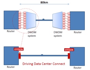 Effdon's CFP does not require the use of external DWDM multiplexing/ demultiplexing and can be added directly onto a router. Source: Effdon Networks
Available 100 Gigabit CFP modules have so far achieved 10km. Now with the Effdon module a 80km reach has been demonstrated that uses 10Gbps optics and no specialist silicon.
Effdon's design is based on the 10x10 MSA (multi-source agreement). "We have managed to resolve the technology barriers - using several techniques - to get to 80km," says Eitan Efron, CEO of Effdon Networks.
There is no 100 Gigabit standard for 80km. The IEEE has two 100 Gigabit standards: the 10km long reach 100GBASE-LR4 and the 40km extended reach 100GBASE-ER4.
Meanwhile, the 100 Gigabit 10x10 MSA based on arrays of 10, 10 Gigabit lasers and detectors, has three defined reaches: 2km, 10km and 40km. At the recent OFC/NFOEC exhibition, Oplink Communication and hybrid integration specialist, Kaiam, showed the 10x10 MSA CFP achieving 40km.
Effdon has not detailed how it has achieved 80km but says its designers have a systems background. "All the software that you need for managing wavelength-division multiplexing (WDM) systems is in our device," says Efron. "Basically we have built a system in a module."
These system elements include component expertise and algorithmic know-how. "Algorithms and software; this is the main IP of the company," says Efron. "We are using 40km components and we are getting 80km."
100 Gigabit landscape
Efron says that while there are alternative designs for 100 Gigabit transmission at 80km or more, each has challenges.
A 100Gbps coherent design achieves far greater reaches but is costly and requires a digital signal processor (DSP) receiver ASIC that consumes tens of watts. No coherent design has yet been implemented using a pluggable module.
Alternative CFP-based 100Gbps direct-detection designs based on a 4x28Gbps architecture exist. But their 28Gbps lanes experience greater dispersion that make achieving 80km a challenge.
MultiPhy's MP1100Q DSP chip counters dispersion. The chip used in a CFP module achieves a 55km point-to-point reach using on-off keying and 800km for dense WDM metro networks using duo-binary modulation.
Finisar and Oclaro also offer 100Gbps direct detection CFP modules for metro dense WDM using duo-binary modulation but without a receiver DSP. ADVA Optical Networking is one system vendor that has adopted such 100Gbps direct-detect modules. Another company developing a 4x28Gbps direct detect module is Oplink Communications.
But Effdon points out that its point-to-point CFP achieves 80km without using an external DWDM multiplexer and demultiplexer - the multiplexing/demultiplexing of the wavelengths is done within the CFP - or external amplification and dispersion compensation. As a result, the CFP plugs straight into IP routers and data centre switches.
"What they [data centre managers] want is what they have today at 10 Gig: ZR [80km] optical transceivers," says Efron

Market demand
"We see a lot of demand for this [80km] solution," says Efron. The design, based on 10 Gigabit optics, has the advantage of using mature high volume components while 25Gbps component technology is newer and available in far lower volumes.
"This [cost reduction associated with volume] will continue; we see 10 Gig lasers going into servers, base stations, data centre switches and next generation PON," says Efron. "Ten Gigabit optical components will remain in higher volume than 25 Gig in the coming years."
The 10x10 MSA CFP design can also be used to aggregate multiple 10 Gig signals in data centre and access networks. This is an emerging application and is not straightforward for the more compact, 4x25Gbps modules as they require a gearbox lane-translation IC.
Reach extension
Effdon Networks' Qbox platform provides data centre managers with 400-800Gbps capacity while offering a reach up to 200km. The box is used with data centre equipment that support CXP or QSFP modules but not the CFP. The 1RU box thus takes interfaces with a reach of several tens of meters to deliver extended transmission.
Qbox supports eight client-side ports - either 40 or 100 Gbps - and four line-facing ports at speeds of 100Gbps or 200Gbps for a reach of 80 to 200km. In future, the platform will deliver 400Gbps line speeds, says Efron.
Samples of the 80km CFP and Qbox are available for selected customers, says Effdon, while general availability of the products will start in the fourth quarter of 2013.

OFC/NFOEC 2013 product round-up - Part 1
Part 1: Client-side transceivers
- First CFP2 single-mode and multi-mode transceiver announcements
- Cisco Systems unveils its CPAK module
- 100 Gigabit QSFPs from Kotura and Luxtera
- CFP2 and 40km CFP 10x10 MSA modules
- Infiniband FDR and 'LR4 superset' QSFPs
The recent OFC/NFOEC exhibition and conference held in Anaheim, California, saw a slew of optical transceiver announcements. The first CFP2 client-side products for single-mode and multi-mode fibre were unveiled by several companies, as was Cisco Systems' in-house CPAK transceiver.
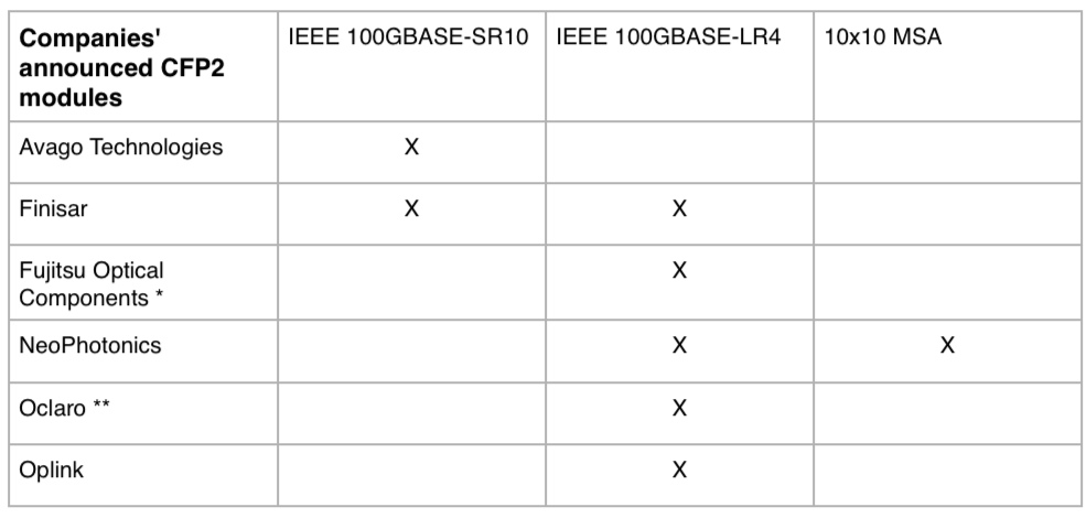
The CFP2 is the pluggable form factor that follows the first generation CFP. The CFP MSA announced the completion of the CFP2 specification at the show, while several vendors including Avago Technologies, Finisar, Fujitsu Optical Components, NeoPhotonics, Oclaro and Oplink Communications detailed their first CFP2 products.
The 40 and 100 Gigabit CFP2 is half the size of the CFP, enabling at least a doubling of the CFP2 transceivers on a faceplate compared to four CFPs (see table below). The CFP2 is also future-proofed to support 200 and 400Gbps (See first comment at bottom of CFP2 story).
Another difference between the CFP and the CFP2 is that the CFP2 uses a 4x25Gbps electrical interface. Accordingly, the CFP2 does not need the 'gearbox' IC that translates between ten, 10 Gigabit-per-second (Gbps) lanes to four, 25Gbps electrical lanes that interface to the 4x25/28Gbps optics. Removing the gearbox IC saves space and reduces the power consumption by several watts.
The industry has long settled on the SFP+ at 10Gbps while the QSFP has become the 40Gbps form factor of choice. With 100Gbps still in its infancy, transceiver vendors are pursuing several client-side interfaces. Much work will be needed to reduce the size, power consumption and cost of 100Gbps interfaces before the industry settles on a single pluggable form factor for the single-mode and multi-mode standards.
CFP2 announcements
Finisar demonstrated two CFP2 modules, one implementing the IEEE 100GBASE-LR4 10km standard and the other, the IEEE 100GBASE-SR10 100m multi-mode standard. The company is using directly-modulated, distributed feedback (DFB) lasers for its CFP2 LR4. In contrast, the CFP module uses more expensive, electro-absorption modulator lasers (EMLs). Finisar demonstrated interoperability between the two LR4 modules, an EML-based CFP and a DFB-based CFP2, at the show.
* An ER4 CFP2 is under development
** Oclaro disclosed indium phosphide components for a future CFP2 line side pluggable
Using directly modulated lasers also reduces the power consumption, says Finisar. Overall, the CFP2 LR4 consumes 7W compared to a 24W first-generation CFP-based LR4.
"We can migrate these [directly modulated laser] designs to a single quad 28 Gig photonic integrated circuit TOSA," says Rafik Ward, Finisar's vice president of marketing. "Likewise on the receive [path], there will be a quad 28 Gig ROSA." The TOSA refers to a transmitter optical sub-assembly while the ROSA is the receiver equivalent. Ward says the CFP2s will be in production this year.
Several module and chip makers took part in the Optical Internetworking Forum's (OIF) multi-vendor demonstration of its 4x25 Gigabit chip-to-module electrical interface, the CEI-28G-VSR. The demonstration included CFP2 LR4s from Finisar and from Oclaro as well as Luxtera's 100Gbps shorter reach module in a QSFP28. Oclaro's CFP2 is expected to be in production in the third quarter of 2013.
Another standard implemented in the CFP2 is the 100GBASE-SR10 multi-mode standard. Avago Technologies and Finisar both detailed CFP2 SR10 modules. The SR10 uses 10 VCSELs, each operating at 10Gbps. The SR10 can be used as a 100Gbps interface or as 10 independent 10Gbps channels.
The CFP2 SR10 can be interfaced to 10 Gigabit Ethernet (GbE) SFP+ modules or combinations of 10GbE SFP+ and 40GbE QSFPs. "What people are looking for using the CFP2 multi-mode module is not only for the 100 Gig Ethernet application but interoperability with 40 Gig Ethernet as well as 10 Gig Ethernet modules," says I Hsing Tan, Ethernet segment marketing manager in the fibre optics product division at Avago.
The SR10 electrical interface specification supports retiming and non-retiming options. The Avago CFP2 module includes clock data recovery ICs that can be used for retiming if needed or bypassed. The result is that Avago's CFP2 SR10 consumes 4-6W, depending on whether the clock data recovery chips are bypassed or used.
Meanwhile, NeoPhotonics became the first company to announce the 10x10 MSA in a CFP2.
NeoPhotonics has not detailed the power consumption but says the 10x10Gbps CFP2 is lower than the CFP since all of the chips - photonic and electrical - are a newer generation and much work has gone into reducing the power consumption.
"Demand is quite strong for the 10x10 solution," says Ferris Lipscomb, vice president of marketing at NeoPhotonics. "The CFP2 version is being developed, and we expect strong demand there as well."
The key advantage of the 10x10-based solution over a 4x25Gbps design is cost, according to NeoPhotonics. "10x10 enjoys the volume and maturity of 10 Gig, and thus the cost advantage," says Lipscomb. "We believe the 10x10 CFP2 will follow the trend of the 10x10 MSA CFP and will offer a significant cost advantage over CFP2 LR4-based solutions."
Cisco's CPAK
Cisco finally showed its in-house silicon photonics-based CPAK transceiver at OFC/NFOEC. The CPAK is the first product to be announced following Cisco's acquisition of silicon photonics player, LightWire.

Cisco says the CPAK is more compact than the CFP2 transceiver with the company claiming that 12 or more transceivers will fit on a faceplate. "While the industry is leapfrogging the CFP with the CFP2, our CPAK leapfrogs the CFP2 because it is much more efficient from a size and power consumption perspective," says Sultan Dawood, a marketing manager at Cisco.
Vendors backing the CFP2 stress that the CPAK is only slighter smaller than the MSA module. "The CFP2 and the CPAK are both interim form factors pending when the CFP4 becomes available." says Avago's Tan. "Any product [like the CFP2] governed by an MSA is going to see strong market adoption."
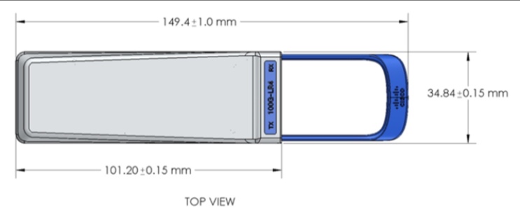 Cisco's CPAK transceiver Source: Cisco
The CFP4 specification is still being worked on but 16 CFP4s will fit on a faceplate and the transceiver is scheduled for the second half of 2014.
At OFC, Cisco demonstrated the CPAK implementing the 100GBASE-LR4 and -SR10 standards. The CPAK transceiver will be generally available in the summer of 2013, says Cisco.
CFP
Oplink Communication and hybrid integration specialist, Kaiam, showed a 100Gbps 10x10 MSA CFP implementing a 40km extended reach.
The 10x10 40km CFP is for connecting data centres and for broadband backhaul applications. The CFP electro-absorption modulator lasers coupled to a wavelength multiplexer make up the TOSA while the ROSA comprises avalanche photodiode receivers and a demultiplexer. Samples will be available in the second quarter of 2013, with production starting in the third quarter.
Source Photonics announced a second-generation 100GBASE-LR4 CFP with a power consumption of 12-14W.
Meanwhile, Effdon Networks detailed its first 100Gbps product, a CFP with a reach of 80km. Until now 100Gbps CFPs have been limited largely to 10km LR4 while the first 100Gbps CFPs with a reach of 80km or greater being 4x25Gbps direct-detection designs that can include specialist ICs.
100 Gig QSFP
Luxtera and Kotura, both detailed 100 Gigabit QSFPs that use their respective silicon photonics technology. The Kotura design uses two chips, has a reach of 2km and is a four-channel wavelength-division multiplexing (WDM) design while the Luxtera design is a four-channel integrated transceiver that uses a single laser and is tailored for 500m although Luxtera says it can achieve a 2km reach.
40 Gigabit Ethernet and Infiniband FDR
Avago Technologies announced that its eSR4 40 Gigabit Ethernet (GbE) QSFP+ has a reach of up to 550m, beyond the reach specified by the IEEE 40GBASE-SR4 standard. The eSR4 supports 40GbE or four independent 10GbE channels. When used as a multi-channel 10GbE interface, the QSFP+ interfaces to various 10GbE form factors such as X2, XFP and SFP+, It can also interface to a 100GbE CFP2, as mentioned.
Avago first announced the eSR4 QSFP+ with a reach of 300m over OM3 multi-mode fibre and 400m over OM4 fibre. The eSR4 now extends the reach to a guaranteed 550m when used with specific OM4 fibre from fibre makers Corning, Commscope and Panduit.
The extended reach is needed to address larger data centres now being build, as well as support flatter switch architectures that use two rather than three tiers of switches, and that have greater traffic flowing between switches on the same tier.
Avago says data centre managers are moving to deploy OM4 fibre. "The end user is going to move from OM3 to OM4 fibre for future-proofing purposes," says Tan. "The next-generation 32 Gig Fibre Channel and 100 Gigabit Ethernet are focussing on OM4 fibre."
Meanwhile, ColorChip showed its 56Gbps QSFP+ implementing the FDR (Fourteen Data Rate) 4x Infiniband standard as part of a Mellanox MetroX long-haul system demonstration at the show.
Finisar also demonstrated a 40Gbps QSFP using four 1310nm VCSELs. The result is a QSFP with a 10km reach that supports a 40Gbps link or four, 10Gbps links when used in a 'breakout' mode. The existing 40GBASE-LR4 standard supports a 40Gbps link only. Finisar's non-standard implementation adds a point-to-multipoint configuration.
"A single form factor port can be used not only for 40 Gig but also can enable higher density 10 Gig applications than what you can do with SFP+," says Ward.
Kaiam detailed a 40Gbps QSFP+ ER4 transceiver having a 40km reach. The QSFP+ transceiver has the equivalent functionality of four DML-based SFP+s fixed on a coarse WDM grid, and includes a wavelength multiplexer and de-multiplexer.
For OFC/NFOEC 2013 - Part 2, click here
Further reading
LightCounting: OFC/NFOEC review: news from the show floor, click here
Ovum: Cisco hits both show hot buttons with silicon photonics for 100G, click here
Kotura demonstrates a 100 Gigabit QSFP
 “QSFP will be the long-term winner at 100 Gig; the same way QSFP has been a high volume winner at 40 Gig”
Arlon Martin, Kotura
The device is aimed at plugging the gap between vertical-cavity surface-emitting laser (VCSEL) -based 100GBASE-SR10 designs that have span 100m, and the CFP-based 100GBASE-LR4 that has a 10km reach.
“It is aimed at the intermediate space, which the IEEE is looking at a new standard for," says Arlon Martin, vice president of marketing at Kotura.
The device is similar to Luxtera's 100 Gigabit-per-second (Gbps) QSFP, also detailed at the OFC/NFOEC 2013 exhibition, and is targeting the same switch applications in the data centre. “Where we differ is our ability to do wavelength-division multiplexing (WDM) on a chip,” says Martin. Kotura also uses third-party electronics such as laser drivers and transimpedance amplifiers (TIA) whereas Luxtera develops and integrates its own.
The Kotura QSFP uses four wavelengths, each at 25Gbps, that operate around 1550nm. “We picked 1550nm because that is where a lot of the WDM applications are," says Martin. “There are also some customers that want more than four channels.” The company says it is also doing development work at 1310nm.
Although Kotura's implementation doesn't adhere to an IEEE standard - the standard is still work in progress - Martin points out that the 10x10 MSA is also not an IEEE standard, yet is probably the best selling client-side 100Gbps interface.
Optical component and module vendors including Avago Technologies, Finisar, Oclaro, Oplink, Fujitsu Optical Components and NeoPhotonics all announced CFP2 module products at OFC/NFOEC 2013. The CFP2 is the next pluggable form factor on the CFP MSA roadmap and is approximately half the size of the CFP.
The advent of the CFP2 enables eight 100Gbps pluggable modules on a system's front panel compared to four CFPs. But with the QSFP, up to 24 modules can be fitted while 48 are possible when mounted double sidedly - ’belly-to-belly’ - across the panel. “QSFP will be the long-term winner at 100 Gig; the same way QSFP has been a high volume winner at 40 Gig,” says Martin.
The QSFP uses 28Gbps pins, which is also called the QSFP28, but Kotura refers to it 100Gbps product as a QSFP. The design consumes 3.5W and uses two silicon photonic chips. Kotura says 80 percent of the total power consumption is due to the electronics.
One of the two chips is the silicon transmitter which houses the platform for the four lasers (gain chips) combined as a four-channel array. Each is an external cavity laser where part of the cavity is within the indium phosphide device and the rest in the silicon photonics waveguide. The gain chips are flip-chipped onto the silicon. The transmitter also includes a grating that sets each laser's wavelength, four modulators, and a WDM multiplexer to combine the four wavelengths before transmission on the fibre.
 Kotura's 4x25 Gig transmitter and receiver chips. Source: Kotura
The receiver chip uses a four-channel demultiplexer with each channel fed to a germanium photo-detector. Two chips are used as it is easier to package each as a transmitter optical sub-assembly (TOSA) or receiver optical sub-assembly (ROSA), says Martin. The 100Gbps QSFP will be generally available in 2014.
Disruptive system design
The recent Compass-EOS IP router announcement is a welcome development, says Kotura, as it brings the optics inside the system - an example of mid-board optics - as opposed to the front panel. Compass-EOS refers to its novel icPhotonics chip combining a router chip and optics as silicon photonics but in practice it is an integrated optics design. The 168 VCSELs and 168 photodetectors per chip is massively parallel interconnect, says Martin.
“The advantage, from our point of view of silicon photonics, is to do WDM on the same fibre in order to reduce the amount of cabling and interconnect needed,” he says. At 100 Gigabit this reduces the cabling by a factor of four and this will grow with more 25Gbps wavelength channels used to 10x or even 40x eventually.
“What we want to do is transition from the electronics to the optical domain as close to those large switching chips as possible,” says Martin. “Pioneers [like Compass-EOS] demonstrating that style of architecture are to be welcomed."
Kotura says that every company that is building large switching and routing ASICs is looking at various interface options. "We have talked to quite a few of them,” says Martin.
One solution suited to silicon photonics is to place the lasers on the front panel while putting the modulation, detection and WDM devices - packaged using silicon photonics - right next to the ASICs. This way the laser works at the cooler room temperature while the rest of the circuitry can be at the temperature of the chip, says Martin.
OFC/NFOEC 2013 to highlight a period of change
Next week's OFC/NFOEC conference and exhibition, to be held in Anaheim, California, provides an opportunity to assess developments in the network and the data centre and get an update on emerging, potentially disruptive technologies.
 Source: Gazettabyte
Several networking developments suggest a period of change and opportunity for the industry. Yet the impact on optical component players will be subtle, with players being spared the full effects of any disruption. Meanwhile, industry players must contend with the ongoing challenges of fierce competition and price erosion while also funding much needed innovation.
The last year has seen the rise of software-defined networking (SDN), the operator-backed Network Functions Virtualization (NFV) initiative and growing interest in silicon photonics.
SDN has already being deployed in the data centre. Large data centre adopters are using an open standard implementation of SDN, OpenFlow, to control and tackle changing traffic flow requirements and workloads.
Telcos are also interested in SDN. They view the emerging technology as providing a more fundamental way to optimise their all-IP networks in terms of processing, storage and transport.
Carrier requirements are broader than those of data centre operators; unsurprising given their more complex networks. It is also unclear how open and interoperable SDN will be, given that established vendors are less keen to enable their switches and IP routers to be externally controlled. But the consensus is that the telcos and large content service providers backing SDN are too important to ignore. If traditional switching and routers hamper the initiative with proprietary add-ons, newer players will willing fulfill requirements.
Optical component players must assess how SDN will impact the optical layer and perhaps even components, a topic the OIF is already investigating, while keeping an eye on whether SDN causes market share shifts among switch and router vendors.
The ETSI Network Functions Virtualization (NFV) is an operator-backed initiative that has received far less media attention than SDN. With NFV, telcos want to embrace IT server technology to replace the many specialist hardware boxes that take up valuable space, consume power, add to their already complex operations support systems (OSS) while requiring specialist staff. By moving functions such as firewalls, gateways, and deep packet inspection onto cheap servers scaled using Ethernet switches, operators want lower cost systems running virtualised implementations of these functions.
The two-year NFV initiative could prove disruptive for many specialist vendors albeit ones whose equipment operate at higher layers of the network, removed from the optical layer. But the takeaway for optical component players is how pervasive virtualisation technology is becoming and the continual rise of the data centre.
Silicon photonics is one technology set to impact the data centre. The technology is already being used in active optical cables and optical engines to connect data centre equipment, and soon will appear in optical transceivers such as Cisco Systems' own 100Gbps CPAK module.
Silicon photonics promises to enable designs that disrupt existing equipment. Start-up Compass-EOS has announced a compact IP core router that is already running live operator traffic. The router makes use of a scalable chip coupled to huge-bandwidth optical interfaces based on 168, 8 Gigabit-per-second (Gbps) vertical-cavity surface-emitting lasers (VCSELs) and photodetectors. The Terabit-plus bandwidth enables all the router chips to be connected in a mesh, doing away with the need for the router's midplane and switching fabric.
The integrated silicon-optics design is not strictly silicon photonics - silicon used as a medium for light - but it shows how optics is starting to be used for short distance links to enable disruptive system designs.
Some financial analysts are beating the drum of silicon photonics. But integrated designs using VCSELs, traditional photonic integration and silicon photonics will all co-exist for years to come and even though silicon photonics is expected to make a big impact in the data centre, the Compass-EOS router highlights how disruptive designs can occur in telecoms.
Market status
The optical component industry continues to contend with more immediate challenges after experiencing sharp price declines in 2012.
The good news is that market research companies do not expect a repeat of the harsh price declines anytime soon. They also forecast better market prospects: The Dell'Oro Group expects optical transport to grow through 2017 at a compound annual growth rate (CAGR) of 10 percent, while LightCounting expects the optical transceiver market to grow 50 percent, to US $5.1bn in 2017. Meanwhile Ovum estimates the optical component market will grow by a mid-single-digit percent in 2013 after a contraction in 2012.
In the last year it has become clear how high-speed optical transport will evolve. The equipment makers' latest generation coherent ASICs use advanced modulation techniques, add flexibility by trading transport speed with reach, and use super-channels to support 400 Gigabit and 1 Terabit transmissions. Vendors are also looking longer term to techniques such as spatial-division multiplexing as fibre spectrum usage starts to approach the theoretical limit.
Yet the emphasis on 400 Gigabit and even 1 Terabit is somewhat surprising given how 100 Gigabit deployment is still in its infancy. And if the high-speed optical transmission roadmap is now clear, issues remain.
OFC/NFOEC 2013 will highlight the progress in 100 Gigabit transponder form factors that follow the 5x7-inch MSA, 100 Gigabit pluggable coherent modules, and the uptake of 100 Gigabit direct-detection modules for shorter reach links - tens or hundreds of kilometers - to connect data centres, for example.
There is also an industry consensus regarding wavelength-selective switches (WSSes) - the key building block of ROADMs - with the industry choosing a route-and-select architecture, although that was already the case a year ago.
There will also be announcements at OFC/NFOEC regarding client-side 40 and 100 Gigabit Ethernet developments based on the CFP2 and CFP4 that promise denser interfaces and Terabit capacity blades. Oclaro has already detailed its 100GBASE-LR4 10km CFP2 while Avago Technologies has announced its 100GBASE-SR10 parallel fibre CFP2 with a reach of 150m over OM4 fibre.
The CFP2 and QSFP+ make use of integrated photonic designs. Progress in optical integration, as always, is one topic to watch for at the show.
PON and WDM-PON remain areas of interest. Not so much developments in state-of-the-art transceivers such as for 10 Gigabit EPON and XG-PON1, though clearly of interest, but rather enhancements of existing technologies that benefit the economics of deployment.
The article is based on a news analysis published by the organisers before this year's OFC/NFOEC event.
OneChip Photonics targets the data centre with its PICs
OneChip Photonics is developing integrated optical components for the IEEE 40GBASE-LR4 and 100GBASE-LR4 interface standards.
The company believes its photonic integrated circuits (PICs) will more than halve the cost of the 40 and 100 Gigabit 10km-reach interfaces, enough for LR4 to cost-competitively address shorter reach applications in the data centre.

"I think we can cut the price [of LR4 modules] by half or better”
Andy Weirich, OneChip Photonics
The products mark an expansion of the Canadian startup's offerings. Until now OneChip has concentrated on bringing PIC-based passive optical network (PON) transceivers to market.
LR4 PICs
The startup is developing separate LR4 transmitter and receiver PICs. The 40 and 100GBASE-LR4 receivers are due in the third quarter of 2012, while the transmitters are expected by the year end.
The 40GBASE-LR4 receiver comprises a wavelength demultiplexer - a 4-channel arrayed waveguide grating (AWG) - and four photo-detectors operating around 1300nm. A spot-size converter - an integrated lens - couples the receiver's waveguide's mode field to the connecting fibre.
"[Data centre operators] are saying that they are having to significantly bend out of shape their data centre architecture to accommodate even 300m reaches”
The 40GBASE-LR4 transmitter PIC comprises four directly-modulated distributed feedback (DFB) lasers while the 100GBASE-LR4 use four electro-absorption modulator DFB lasers. Different lasers for the two PICs are required since the four wavelengths at 100 Gig, also around 1300nm, are more tightly spaced: 5nm versus 20nm. "They are much closer together than the 40 Gig version,” says Andy Weirich, OneChip Photonics' vice president of product line management.
Another consequence of the wider wavelength spacings is that the 40 Gig transmitter uses four discrete lasers. “Because the 40 Gig wavelengths are much further apart, putting all the lasers on the one die is problematic," says Weirich. The 40GBASE-LR4 design thus uses five indium phosphide components: four lasers and the AWG, while the 40GBASE-LR4 receiver and the two 100GBASE-LR4 devices are all monolithic PICs.
Both LR4 transmitter designs also include monitor photo-diodes for laser control
Lower size and cost
OneChip says the resulting PICs are tiny, measuring less than 3mm in length. “We think the PICs will enable the packaging of LR4 in a QSFP,” says Weirich. 40GBASE-LR4 products already exists in the QSFP form factor but the 100GBASE-LR4 uses a CFP module.
The startup expects module makers to use its receiver chips once they become available rather than wait for the receiver-transmitter PIC pair. "Reducing the size of one half the solution is possibly good enough to fit the whole hybrid design - the PIC for the receive and discretes for the transmit - into a QSFP,” says Weirich.
The PICs are expected to reduce significantly the cost of LR4 modules. "I think we can cut the price by half or better,” says Weirich. “Right now the LR4 is far too expensive to be used for data centre interconnect.” OneChip expects its LR4 PICs to be cost-competitive with the 2km reach 10x10 MSA interface.
Meanwhile, short-reach 40 and 100 Gig interfaces use VCSEL technology and multi-mode fibre to address 100m reach requirements. In larger data centres this reach is limiting. Extended reach - 300-400m - multimode interfaces have emerged but so far these are at 40 Gig only.
"[Data centre operators] are saying that they are having to significantly bend out of shape their data centre architecture to accommodate even 300m reaches,” says Weirich. “They really want more than that.”
OneChip believes interfaces distances of 200m-2km is underserved and it is this market opportunity that it is seeking to address with its LR4 designs.
Roadmap
Will OneChip integrate the design further to product a single PIC LR4 transceiver?
"It can be put into one chip but it is not clear that there is an economic advantage,” says Weirich. Indeed one PIC might even be more costly than the two-PIC chipset.
Another factor is that at 100 Gig, the 25Gbps electronics present a considerable signal integrity design challenge. “It is very important to keep the electronics very close to the photo-detectors and the modulators,” he says. “That becomes more difficult if you put it all on the one chip.” The fabrication yield of a larger single PIC would also be reduced, impacting cost.
OneChip, meanwhile, has started limited production of its PON optical network unit (ONU) transceivers based on its EPON and GPON PICs. The company's EPON transceivers are becoming generally available while the GPON transceivers are due in two months’ time.
The company has yet to decide whether it will make its own LR4 optical modules. For now OneChip is solely an LR4 component supplier.
Further reading:
See OFC/ NFOEC 2012 highlights, the Kotura story in the Optical Engines section
Challenges, progress & uncertainties facing the optical component industry
In recent years the industry has moved from direct detection to coherent transmission and has alighted on a flexible ROADM architecture. The result is a new level in optical networking sophistication. OFC/NFOEC 2012 will showcase the progress in these and other areas of industry consensus as well as shining a spotlight on issues less clear.
Optical component players may be forgiven for the odd envious glance towards the semiconductor industry and its well-defined industry dynamics.
The semiconductor industry has Moore’s Law that drives technological progress and the economics of chip-making. It also experiences semiconductor cycles - regular industry corrections caused by overcapacity and excess inventory. The semiconductor industry certainly has its challenges but it is well drilled in what to expect.
Optical challenges
The optical industry experienced its own version of a semiconductor cycle in 2010-11 - strong growth in 2010 followed by a correction in 2011. But such market dynamics are irregular and optical has no Moore's Law.
Optical players must therefore work harder to develop components to meet the rapid traffic growth while achieving cost efficiencies, denser designs and power savings.
Such efficiencies are even more important as the marketplace becomes more complex due to changes in the industry layers above components. The added applications layer above networks was highlighted in the OFC/NFOEC 2012 news analysis by Ovum’s Karen Liu. The analyst also pointed out that operators’ revenues and capex growth rates are set to halve in the years till 2017 compared to 2006-2010.
Such is the challenging backdrop facing optical component players.
Consensus
Coherent has become the defacto standard for long-haul high-speed transmission. Optical system vendors have largely launched their 100Gbps systems and have set their design engineers on the next challenge: addressing designs for line rates beyond 100Gbps.
Infinera detailed its 500Gbps super-channel photonic integrated circuit last year. At OFC/NFOEC it will be interesting to learn how other equipment makers are tackling such designs and what activity and requests optical component vendors are seeing regarding the next line rates after 100Gbps.
Meanwhile new chip designs for transport and switching at 100Gbps are expected at the show. AppliedMicro is sampling its gearbox chip that supports 100 Gigabit Ethernet and OTU4 optical interfaces. More announcements should be expected regarding merchant 100Gbps digital signal processing ASIC designs.
An architectural consensus for wavelength-selective switches (WSSes) - the key building block of ROADMs - are taking shape with the industry consolidating on a route-and-select architecture, according to analysts.
Gridless - the ROADM attribute that supports differing spectral widths expected for line rates above 100Gbps - is a key characteristic that WSSes must support, resulting in more vendors announcing liquid crystal on silicon designs.
Client-side 40 and 100 Gigabit Ethernet (GbE) interfaces have a clearer module roadmap than line-side transmission. After the CFP comes the CFP2 and CFP4 which promise denser interfaces and Terabit capacity blades. Module form factors such as the QSFP+ at 40GbE and in time 100GbE CFP4s require integrated photonic designs. This is a development to watch for at the show.
Others areas to note include tunable-laser XFPs and even tunable SFP+, work on which has already been announced by JDS Uniphase.
Lastly, short-link interfaces and in particular optical engines is another important segment that ultimately promises new system designs and the market opportunity that will unleash silicon photonics.
Optical engines can simplify high-speed backplane designs and printed circuit board electronics. Electrical interfaces moving to 25Gbps is seen as the threshold trigger when switch makers decide whether to move their next designs to an optical backplane.
The Optical Internetworking Forum will have a Physical and Link Layer (PLL) demonstration to showcase interoperability of the Forum’s Common Electrical Interface (CEI) 28Gbps Very Short Reach (VSR) chip-to-module electrical interfaces, as well as a demonstration of the CEI-25G-LR backplane interface.
Companies participating in the interop include Altera, Amphenol, Fujitsu Optical Components, Gennum, IBM, Inphi, Luxtera, Molex, TE Connectivity and Xilinx.
Altera has already unveiled a FGPA prototype that co-packages 12x10Gbps transmitter and receiver optical engines alongside its FPGA.
Uncertainties
OFC/NFOEC 2012 also provides an opportunity to assess progress in sectors and technology where there is less clarity. Two sectors of note are next-generation PON and the 100Gbps direct-detect market.
For next-generation PON, several ideas are being pursued, faster extensions of existing PON schemes such as a 40Gbps version of the existing time devision multiplexing PON schemes, 40G PON based on hybrid WDM and TDM schemes, WDM-PON and even ultra dense WDM-PON and OFDM-based PON schemes.
The upcoming show will not answer what the likely schemes will be but will provide an opportunity to test what the latest thinking is.
The same applies for 100 Gigabit direct detection.
There are significant cost advantages to this approach and there is an opportunity for the technology in the metro and for data centre connectivity. But so far announcements have been limited and operators are still to fully assess the technology. Further announcements at OFC/NFOEC will highlight the progress being made here.
The article has been written as a news analysis published by the organisers before this year's OFC/NFOEC event.
40 Gigabit Ethernet QSFPs boost port density and reach
 "For the larger data centres being built today, reach is becoming more and more important"
I Hsing Tan, Avago
Avago’s eSR4 QSFP+ transceiver extends the reach of 40GbE over multimode fibre beyond the IEEE 40GBASE-SR4 specification, to 300m over OM3 and 400m over OM4 multimode fibre.
Reflex Photonics’ 40GbE QSFP also achieves 300m over OM3 fibre and while it has not tested the transceiver over OM4 fibre, the company is using the same optics that it uses for its CFP which meets 450m over OM4.
“This [QSFP] is aimed at large data centres operated by the likes of a Google or a Facebook,” says Robert Coenen, vice president, sales and marketing at Reflex Photonics. Such data centres can have link requirements of 1000m. “The more reach you can give over multimode fibre, the more money they [data centre operators] can save.”
The eSR4, like Avago's already announced iSR4 (interoperable SR4) 40GbE QSFP+ transceiver, supports either 40GbE or four independent 10GbE channels. When used as a multichannel 10GbE interface, the QSFP+ can interface to various 10GbE form factors such as X2, XFP and SFP+, says Avago.
The iSR4 also increases the faceplate port density of equipment from 48, 10 Gigabit Ethernet (GbE) SFP+ ports to up to 44 QSFP+ 40GbE ports. Avago says that one equipment vendor has already announced a card with 36 QSFP+ ports. The iSR4 QSFP+ also reduces the overall Gigabit/Watt power consumption to 37.5mW/Gbps compared to 100mW /Gbps for the SFP+. The eSR4 has half the power consumption, which puts it around 50mW/Gbps.
But the iSR4 matches the reach of the IEEE 40GBASE-SR4 40GbE standard: 100m for OM3 and 150m for OM4-based fibre. "This [reduced reach at 40GbE] creates an issue for data centre operations," says I Hsing Tan, Ethernet segment marketing manager in the fiber optics product division at Avago. "They require additional investment to redo all the wiring in current 10GbE infrastructure to support a shorter reach."
With the extended reach 40GbE QSFPs the reach associated with 10GbE interfaces on OM3 and OM4 multimode fibre is now restored.
The iSR4 module is available now, says Avago, while the eSR4 will be available from mid-2012. Reflex’s Coenen says it will have samples of its 40GbE QSFP, which also supports 40GbE and 4x10GbE, by May 2012.
What has been done
For Avago's iSR4 QSFP+ to operate as four, 10GbE channels, it has to comply with the 10GBASE-SR optical standard. That is because 10GBASE-SR supports a maximum receive power of -1dBm whereas the 40GBASE-SR4 has a maximum output power of 2.4dBm. The transmitter power of the iSR4 has thus been reduced. "We force the output of the transmitter down to -1dBm," says Tan.
To achieve the greater reach, the eSR4 uses a VCSEL design with a tighter spectral width. Other parameters include the optical modulation amplitude power and the wavelength. These affect the resulting fibre dispersion. “Once you control the spectral width, you can design the other two to meet the specs," says Tan.
The Avago 40GbE QSFP+ modules use an integrated 4- channel VCSEL array and a 4-channel photo-detector array.
Significance
The 40GbE short reach interfaces play an important role in the data centre. As servers move from using 1GbE to 10GbE interfaces, the uplink from aggregation 'top-of-rack' switches must also scale from 10GbE to higher speeds of 40GbE or 100GbE.
However existing 100GbE interfaces make use of the CFP module which is relatively large and expensive. And although the 100GbE standard has a clear roadmap leading to CFP2 and CFP4 modules, half and a quarter of the size of the CFP, respectively, these are not yet available.
40GbE QSFP+ transceivers do exist and offer the equipment faceplate density improvement vendors want.
The QSFP+ also benefits existing 10GbE designs by supporting nearly 4x the number of 10GbE on a card. Thus a new blade supporting up to 44, 40GbE QSFP+ transceivers can interface to up to 176 10GbE transceivers, a near fourfold capacity increase.
According to Avago, between 10% and 20% of interface requirements in the data centre are beyond 150m. Without the advent of extended reach 40GbE modules, data centre operators would need to deploy single mode fibre and a 40GBASE-LR4 module, it says. And while that can be fitted inside a QSFP, its power consumption is up to 3.5W, compared to the 1.5W of the QSFP+ eSR4. "The cost of the LR4 is also increased by at least a factor of three," says Tan.
Avago says that some 95% of all fibre in the data centre is multimode fibre. As for OM3 and OM4 deployments the ratio is 80% to 20%, respectively.