
How CPO enables disaggregated computing

A significant shift in cloud computing architecture is emerging as start-up Drut Technologies introduces its scalable computing platform. The platform is attracting attention from major banks, telecom providers, and hyperscalers.
At the heart of this innovation is a disaggregated computing system that can scale to 16,384 accelerator chips, enabled by pioneering use of co-packaged optics (CPO) technology.
“We have all the design work done on the product, and we are taking orders,” says Bill Koss, CEO of Drut (pictured).
System architecture
The start-up’s latest building block as part of its disaggregated computing portfolio is the Photonic Resource Unit 2500 (PRU 2500) chassis that hosts up to eight double-width accelerator chips. The chassis also features Drut’s interface cards that use co-package optics to link servers to the chassis, link between the chassis directly or, for larger systems, through optical or electrical switches.
The PRU 2500 chassis supports various vendors’ accelerator chips: graphics processing units (GPUs), chips that combine general processing (CPU) and machine learning engines, and field programmable gate arrays (FPGAs).
Drut has been using third-party designs for its first-generation disaggregated server products. More recently the start-up decided to develop its own PRU 2500 chassis as it wanted to have greater design flexibility and be able to support planned enhancements.
Koss says Drut designed its disaggregated computing architecture to be flexible. By adding photonic switching, the topologies linking the chassis, and the accelerator chips they hold, can be combined dynamically to accommodate changing computing workloads.
Up to 64 racks – each rack hosting eight PRU 2500 chassis or 64 accelerator chips – can be configured as a 4096-accelerator chip disaggregated compute cluster. Four such clusters can be networked together to achieve the full 16,384 chip cluster. Drut refers to its compute cluster concept as the DynamicXcelerator virtual POD architecture.

The architecture can also be interfaced to an enterprise’s existing IT resources such as Infiniband or Ethernet switches. “This set-up has scaling limitations; it has certain performance characteristics that are different, but we can integrate existing networks to some degree into our infrastructure,” says Koss.
PRU-2500
The PRU 2500 chassis is designed to support the PCI Express 5.0 protocol. The chassis supports up to 12 PCIe 5.0 slots, including eight double-width slots to host PCIe 5.0-based accelerators. The chassis comes with two or four tFIC 2500 interface cards, discussed in the next section.
The remaining four of the 12 PCIe slots can be used for single-width PCIe 5.0 cards or Drut’s rFIC-2500 remote direct memory access (RDMA) network cards for optical-based accelerator-to-accelerator data transfers.
Also included in the PRU 2500 chassis are two large Broadcom PEX89144 PCIe 5.0 switch chips. Each PEX chip can switch 144 PCIe 5.0 lanes for a total bandwidth of 9.2 terabits-per-second (Tbps).

Co-packaged optics and photonic switching
The start-up is a trailblazer in adopting co-packaged optics. Due to the input-output requirements of its interface cards, Drut chose to use co-packaged optics since traditional pluggable modules are too bulky and cannot meet the bandwidth density requirements of the cards.
There are two types of interface cards. The iFIC 2500 is added to the host while the tFIC 2500 is part of the PRU 2500 chassis, as mentioned. Both cards are a half-length PCIe Gen 5.0 card and each has two variants: one with two 800-gigabit optical engines to support 1.6Tbps of I/O and one with four engines for 3.2Tbps I/O. It should be noted that these cards are used to carry PCIe 5.0 lanes, each lane operating at 32 gigabits-per-second (Gbps) using non-return-to-zero (NRZ) signalling.
The cards interface to the host server and connect to their counterparts in other PRU 2500 chassis. This way, the server can interface with as accelerator resources across multiple PRU 2500s.
Drut uses co-packaged optics engines due to their compact size and superior bandwidth density compared to traditional pluggable optical modules. “Co-package optics give us a high amount of density endpoints in a tiny physical form factor,” says Koss.
The co-packaged optics engines include integrated lasers rather than using external laser sources. Drut has already sourced the engines from one supplier and is also waiting on sources from two others.
“The engines are straight pipes – 800 gigabits to 800 gigabits,” says Koss. “We can drop eight lasers anywhere, like endpoints on different resource modules.”

Drut also uses a third-party’s single-mode-fibre photonic switch. The switch can be configured from 32×32 up to 384×384 ports. Drut will talk more about the photonic switching aspect of its design later this year.
The final component that makes the whole system work is Drut’s management software, which oversees the system’s traffic requirements and the photonic switching. The complete system architecture is shown below.

More development
Koss says being an early adopter of co-package optics has proven to be a challenge.
The vendors are still at the stage of ramping up volume manufacturing and resolving quality and yield issues. “It’s hard, right?” he says,
Koss says WDM-based co-packaged optics are 18 to 24 months away. Further out, he still foresees photonic switching of individual wavelengths: “Ultimately, we will want to turn those into WDM links with lots of wavelengths and a massive increase in bandwidth in the fibre plant.”
Meanwhile, Drut is already looking at its next PRU chassis design to support the PCIe 6.0 standard, and that will also include custom features driven by customer needs.
The chassis could also feature heat extraction technologies such as water cooling or immersion cooling, says Koss. Drut could also offer a PRU filled with CPUs or a PRU stuffed with memory to offer a disaggregated memory pool.
“A huge design philosophy for us is the idea that you should be able to have pools of GPUs, pools of CPUs, and pools of other things such as memory,” says Koss. “Then you compose a node, selecting from the best hardware resources for you.”
This is still some way off, says Koss, but not too far out: “Give us a couple of years, and we’ll be there.”
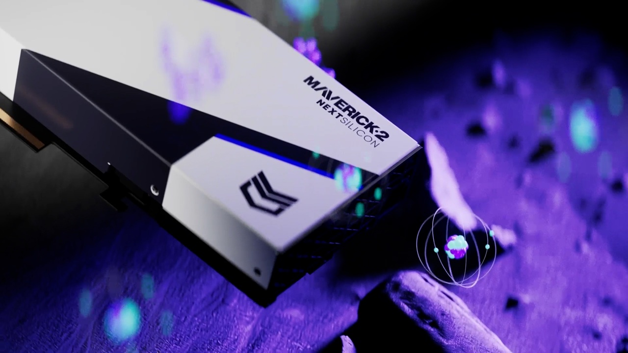
NextSilicon’s Maverick-2 locks onto bottleneck code
- NextSilicon has developed a novel chip that adapts its hardware to accelerate high-performance computing applications.
- The Maverick-2 is claimed to have up to 4x the processing performance per watt of graphics processing units (GPUs) and 20x that of high-performance general processors (CPUs).
After years of work, the start-up NextSilicon has detailed its Maverick-2, what it claims is a new class of accelerator chip.
A key complement to the chip is NextSilicon’s software, which parses the high-performance computing application before mapping it onto the Maverick-2.
“CPUs and GPUs treat all the code equally,” says Brandon Draeger, vice president of marketing at NextSilicon. “Our approach looks at the most important, critical part of the high-performance computing application and we focus on accelerating that.”
With the unveiling of the Maverick-2 NextSilicon has exited its secrecy period.
Founded in 2017, the start-up has raised $303 million in funding and has 300 staff. The company is opening two design centres—in Serbia and Switzerland—with a third planned for India. The bulk of the company’s staff is located in Israel.
High-performance computing and AI
High-performance computing simulates complex physical processes such as drug design and weather forecasting. Such computations require high-precision calculations and use 32-bit or 64-bit floating-point arithmetic. In contrast, artificial intelligence (AI) workloads have more defined computational needs, and can use 16-bit and fewer floating-point formats. Using these shorter data formats results in greater parallelism per clock cycle.
Using NextSilicon’s software, a high-performance computing workload written in such programming languages as C/C++, Fortran, OpenMP, or Kokkos, is profiled to identify critical flows. These are code sections that run most frequently and benefit from acceleration.
“We look at the most critical part of the high-performance computing application and focus on accelerating that,” says Draeger.
This is an example of the Pareto principle: a subset of critical code (the principle’s 20 per cent) that runs most (80 per cent) of the time. The goal is to accelerate these most essential code segments.
The Maverick-2
These code flows are mapped onto the Maverick-2 processor and replicated hundreds or thousands of times, depending on their complexity and the on-chip resources available.
However, this is just the first step. “We run telemetry with the application,” says Draeger. “So, when the chip first runs, the telemetry helps us to size and identify the most likely codes.” The application’s mapping onto the hardware is then refined as more telemetry data is collected, further improving performance.
“In the blink of an eye, it can reconfigure what is being replicated and how many times,” says Draeger. “The more it runs, the better it gets.”
 Source: NextSilicon
The time taken is a small fraction of the overall run time (see diagram). “A single high-performance computing simulation can run for weeks,” says Draeger. “And if something significant changes within the application, the software can help improve performance or power efficiency.”
NextSilicon’s software saves developers months of effort when porting applications ported onto a high-performance computing accelerator, it says.
NextSilicon describes the Maverick-2 as a new processor class, which it calls an Intelligent Compute Accelerator (ICA). Unlike a CPU or GPU, it differentiates the code and decides what is best to speed up. The configurable hardware of the Maverick-2 is thus more akin to a field-programmable gate array (FPGA). But unlike an FPGA, the Maverick-2’s hardware adapts on the fly.
Functional blocks and specifications
The Maverick-2 is implemented using a 5nm CMOS process and is based on a dataflow architecture. Its input-output (I/O) includes 16 lanes of PCI Express (PCIe 5.0) and a 100 Gigabit Ethernet interface. The device features 32 embedded cores in addition to the main silicon logic onto which the flows are mapped. The chip’s die is surrounded by four stacks of high-bandwidth memory (HBM3E), providing 96 gigabytes (GB) of high-speed storage.
NextSilicon is also developing a dual-die design – two Maverick-2s combined – designed with the OCP Acceleration Module (OAM) packaged form factor in mind. The OAM variant, arriving in 2025, will use HBM3E memory for an overall store capacity of 192 gigabytes (GB) (see diagram).
 Source: NextSilicon
The OCP, the open-source industry organisation, has developed an open-source Universal Base Board (OBB) specification that hosts up to eight such OAMs or, in this case, Maverick-2s. NextSilicon is aiming to use the OAM dual-die design for larger multi-rack platforms.
The start-up says it will reveal the devices’ floating-point operations per second (FLOPS) processing performance and more details about the chip’s architecture in 2025.
 Source: NextSilicon

Partners
NextSilicon has been working with vendor Penguin Solutions to deliver systems that integrated their PCI Express modules based on its first silicon, the Maverick-1, a proof-of-concept design. Sandia National Laboratories led a consortium of US labs, including Lawrence Livermore National Laboratory and Los Alamos National Laboratory, in trialling the first design.
“We’re currently sampling dozens of customers across national labs and commercial environments. That’s been our focus,” says Draeger. “We have early-adopter programs that will be available at the start of 2025 with Dell Technologies and Penguin Solutions, where customers can get engaged with an evaluation system.”
Volume production is expected by mid-2025.
Next steps
AI and high-performance computing are seen as two disparate disciplines, but Draeger says AI is starting to interact with the latter in exciting ways.
Customers may pre-process data sets using machine-learning techniques before running a high-performance computing simulation. This is referred to as data cleansing.
A second approach is the application of machine-learning to the simulation’s results for post-processing analysis. Here, the simulation results are used to improve AI models that aim to approximate what a simulation is doing, to deliver results deemed ‘good enough’. Weather forecasting is one application example.
An emerging approach is to run small AI models in parallel with the high-performance simulation. “It offers a lot of promise for longer-running simulations that can take weeks, to ensure that the simulation is on track,” says Draeger.
Customers welcome anything that speeds up the results or provides guidance while the calculations are taking place.
NextSilicon is focussing on HPC but is eyeing data centre computing.
“We’re starting with HPC because that market has many unique requirements, says Draeger. “If we can deliver performance benefits to high-performance computing customers then AI is quite a bit simpler.”
There is a need for alternative accelerator chips that are flexible, power efficient, and can adapt in whatever direction a customer’s applications or workloads take them, says Draeger.
NextSilicon is betting that its mix of software and self-optimising hardware will become increasingly important as computational needs evolve.

PCI Express back on track with latest specifications
Richard Solomon and Scott Knowlton are waiting for me in the lobby of a well-known Tel-Aviv hotel overseeing the sunlit Mediterranean Sea.
 Richard SolomonSolomon, vice chair of the PCI Special Interest Group (PCI-SIG), and Knowlton, its marketing working group co-chair, are visiting Israel to deliver a training event addressing the PCI Express (PCIe) high-speed serial bus standard.
With over 750 member companies, PCI-SIG conducts several training events around the world each year. The locations are chosen where there is a concentration of companies and engineers undertaking PCIe designs. “These are chip, board and systems architects,” says Solomon.
PCI-SIG has hit its stride after a prolonged quiet period. The group completed the PCIe 4.0 standard in 2017, seven years after it launched PCIe 3.0. The PCIe 4.0 doubles the serial bus speed and with the advent of PCIe 5.0, it will double again.
“We were late with PCIe 4.0,” admits Solomon. But with the introduction of the PCIe 5.0 standard in the first quarter of 2019, the serial bus’ speed progression will be back on track. “PCIe 5.0 is where the industry needs it to be.”
The latest training event is addressing the transition to PCIe 5.0. “User implementation stuff; the PHY, controller and verification IP,” says Knowlton. Verification IP refers to the protocols and interfaces needed to verify a PCIe 5.0-enabled chip design.
Markets
PCIe is used in a range of industries. In the cloud, the serial bus is used for servers and storage.
For servers, PCIe has been adopted by general-purpose microprocessors and more specialist devices such as FPGAs, graphics processing units and AI hardware.
The technology is also being used by enterprises, with PCIe switch silicon adopted in data centres to enable server redundancy and failover.
PCIe 5.0 is where the industry needs it to be
PCIe is also being used for storage and in particular solid-state drives (SSDs). That is because PCIe 4.0 transfers data at 16 gigabit-per-second (Gbps) per lane and can be scaled in parallel, typically in a by-four (x4) or a by-16 (x16) lane configuration.
The proportion of the SSDs that use PCIe is expected to grow from a quarter in 2018 to over three quarters in 2022, according to Forward Insights. Meanwhile, IDC forecasts that the SSD market will grow at a compound annual growth rate of 15 percent from 2016 to 2021.
PCIe is also employed within mobile handsets and for the Internet of Things designs. PCI-SIG attributes its adoption for these applications due to its speed and lane-width flexibility as well as its power efficiency.
 Source: PCI-SIG
Bus specifications
The PCIe bus uses point-to-point communications. The standard uses a simple duplex scheme - serial transmissions in both directions that is referred to as a lane. The bus can be bundled in a variety of lane configurations - x1, x2, x4, x8, x12, x16 and x32 - although x2, x12 and x32 are rarely, if ever, used in practice.
 Scott KnowltonThe first two iterations of PCIe, versions 1.0 and 2.0, delivered 2.5 and 5 gigatransfers-per-second (GT/s) per lane per direction, respectively.
A transfer refers to an encoded bit. The first two PCIe versions use an 8b/10b encoding scheme such that for every ten-bit payload sent, only 8 bits are data. This is why the data transfer rates per lane per direction are 2Gbps and 4Gbps (250 and 500 gigabytes-per-second), respectively (see table).
With PCIe 3.0, the decision was made to increase the transfer rate to 8GT/s per lane based on the assumption that no equalisation would be needed to counter inter-symbol interference at that speed, says Solomon. However, equalisation was needed in the end but that explains why PCIe 3.0 adopted 8GT/s and not 10GT/s.
Another PCIe 3.0 decision was to move to a 128b/130b scheme to reduce the encoding overhead from 20 percent to just over 1 percent. This is why the transfer rate and bit rate are almost equal from the PCIe 3.0 standard onwards (see table).
The recent PCIe 4.0 specification doubles the transfer rate from 8GT/s to 16GT/s while PCIe 5.0 will achieve 32GT/s per lane per direction.
When more than one lane is used, the encoded data is distributed across the lanes. A PCIe controller is used at each end of a lane to make sense of the bits. Meanwhile, a PCIe switch, a separate chip, can be used when fan out is needed to distribute the point-to-point links.
Compliance testing and design issues
Compliance testing of PCIe 4.0 will only occur in the beginning of 2019 even though it was standardised in 2017. Solomon says that this length of time is actually one of PCI-SIG's shorter periods. It takes time to refine the exact electrical testing to be used, he sys, and there is only so much that can be done until the silicon arrives.
Given that there are now 28Gbps and 56Gbps serialiser-deserialiser (serdes) technologies available, why were the PCIe 4.0 and PCIe 5.0 lane speeds not faster? Solomon says the latest PCIe standards were chosen to be multiples of the PCIe 3.0’s 8GT/s lane speed to ensure backward compatibility.
That said, designing systems using PCIe 4.0 and PCIe 5.0 signalling speeds is a challenge. Printed circuit boards need to be multi-layer and used higher-quality materials while retimer ICs are needed to achieve signal distances of 20 inches.
Solomon stresses that not all systems required such signal reaches; the dense electronics being developed for automotives that use AI techniques to make sense of their environment being one such example.
And with that, Solomon apologises and gets up: “I have a session to present”.