
The long arm of PCI Express
- Optical is being added as a second physical medium to the PCI Express (PCIe) data transfer protocol.
- PCI Express is an electrical standard, but now the Peripheral Component Interconnect Special Interest Group (PCI-SIG) has created a working group to standardise PCIe’s delivery optically.
- PCI-SIG is already developing copper cabling specifications for the PCI Express 5.0 and 6.0 standards.
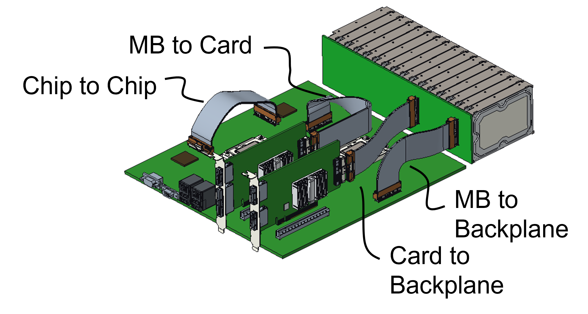
Since each generation of PCIe doubles the data transfer rate, PCI-SIG member companies want copper cabling to help with the design of high-speed PCIe interconnects on a printed circuit board (PCB), between PCBs, and between racks (see diagram).
“We’ve seen a lot of interest over recent months for an optical cable that will support PCI Express,” says Al Yanes, PCI-SIG president and chairperson.
He cites the trends of the decreasing cost and size of optics and how silicon photonics enables the adding of optics alongside ASICs.
“We have formed a workgroup to deliver an optical cable,” says Yanes. “There are many applications, but one is a longer-distance reach for PCI Express.”
“It is a void in the market [the lack of optical support for PCIe], and it needs to be filled,” says Bill Koss, CEO of Drut Technologies. “These efforts tend to take longer than estimated, so better to start sooner.”
Drut has developed a PCIe over photonics solution as part of its photonic direct connect fabric for the data centre.
The data centre is going photonic, says Koss, so there is a need for such working standards as photonics get closer to processors.
The PCIe protocol
PCIe is used widely across many industries.
In the data centre, PCIe is used by general-purpose microprocessors and accelerator chips, such as FPGAs, graphics processing units and AI hardware, to connect to storage and network interface cards.
The PCIe bus uses point-to-point communications based on a simple duplex scheme – serial transmissions in both directions which is referred to as a lane.
The bus can be bundled in various lane configurations – x1, x2, x4, x8, x12, x16 and x32 – with x4, x8 and x16 the configurations most used.
The first two PCIe versions, 1.0 and 2.0, delivered 2.5 and 5 giga transfers-per-second (GT/s) per lane per direction, respectively.
A transfer refers to an encoded bit. The first two PCIe versions use an 8b/10b encoding scheme such that for every ten-bit payload sent, 8 bits are data. This is why the data transfer rates per lane per direction are 2Gbps and 4Gbps (250 and 500 gigabytes per second), respectively.
With PCIe 3.0, the decision was made to increase the transfer rate to 8GT/s per lane, which assumed that no equalisation would be needed to counter inter-symbol interference at that speed. However, equalisation was required, which explains why PCIe 3.0 adopted 8GT/s and not 10GT/s.
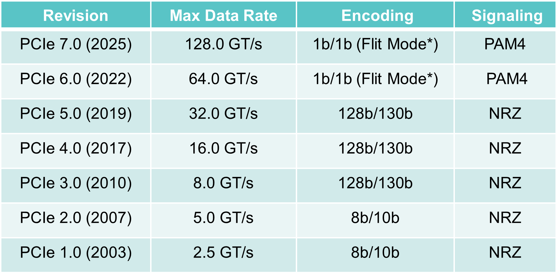
Another PCIe 3.0 decision was to move to a 128b/130b scheme to reduce the encoding overhead from 20 per cent to over 1 per cent. Now the transfer and bit rates are almost equal from the PCIe 3.0 standard onwards.
PCIe 4.0 doubles the transfer rate from 8GT/s to 16GT/s, while PCIe 5.0 is 32GT/s per lane per direction.
Since then, PCIe 6.0 has been specified, supporting 64GT/s per lane per direction. PCIe 6.0 is the first standard for 4-level pulse amplitude modulation (PAM4) signalling.
Now the PCIe 7.0 specification work is at version 0.3. PCIe 7.0 uses PAM-4 to deliver 128GT/s per lane per direction. The standard is expected to be completed in 2025, with industry adoption in 2027.
Optical cabling for PCIe
The PCI Express 5.0 and 6.0 copper cabling specifications are expected by the year-end. The expected distance using copper cabling and retimers is 5-6m.
The reach of an optical PCIe standard will ‘go a lot further’ than that, but how far is to be determined.
Yanes says optical cables for PCIe will also save space: “An optical cable is not as bulky nor as thick as a copper cable.”
Whether the optical specification work will support all versions of PCIe is to be determined.
“There’s some interest to support them all; the copper solution supports all the negotiations,” says Yanes. “It’s something that needs to be discussed, but, for sure, it will be the higher speeds.”
The working group will decide what optical options to specify. “We know that there are some basic things that we need to do to PCI Express technology to make it support optics,” says Yanes.
The working group aims to make the specification work generic enough that it is ‘optical friendly’.
“There are many optical techniques in the industry, and there is discussion as to which of these optical techniques is going to be the winner in terms of usage,” says Yanes. “We want our changes to make PCI Express independent of that discussion.”
The organisation will make the required changes to the base specification of PCIe to suit optical transmission while identifying which optical solutions to address and build.
PCI-SIG will use the same Flit Mode and the same link training, for example, while the potential specification enhancements include coordinating speed transitions to match the optics, making side-band signals in-band, and making the specification more power-efficient given the extended reach.
Pluggable optical modules, active optical cables, on-board optics, co-packaged optics and optical input-output are all optical solutions being considered.
An optical solution for PCIe will also benefit technologies such as Compute Express Link (CXL) and the Non-Volatile Memory Express (NVMe) protocols implemented over PCIe. CXL, as it is adopted more broadly, will likely drive new uses that will need such technology.
The PCIe optical working group will complete the specifications in 12-18 months. Yanes says a quicker working solution may be offered before then.

PCI-SIG releases the next PCI Express bus specification

The Peripheral Component Interconnect Express (PCIe) 6.0 specification doubles the data rate to deliver 64 giga-transfers-per-second (GT/s) per lane.
For a 16-lane configuration, the resulting bidirectional data transfer capacity is 256 gigabytes-per-second (GBps).
“We’ve doubled the I/O bandwidth in two and a half years, and the average pace is now under three years,” says Al Yanes, President of the Peripheral Component Interconnect – Special Interest Group (PCI-SIG).
The significance of the specification’s release is that PCI-SIG members can now plan their products.
Users of FPGA-based accelerators, for example, will know that in 12-18 months there will be motherboards running at such rates, says Yanes
Applications
The PCIe bus is used widely for such applications as storage, processors, artificial intelligence (AI), the Internet of Things (IoT), mobile, and automotive.
In servers, PCIe has been adopted for storage and by general-purpose processors and specialist devices such as FPGAs, graphics processor units (GPUs) and AI hardware.
The CXL standard enables server disaggregation by interconnecting processors, accelerator devices, memory, and switching, with the protocol sitting on top of the PCIe physical layer. The NVM Express (NVMe) storage standard similarly uses PCIe.
“If you are on those platforms, you know you have a healthy roadmap; this technology has legs,” says Yanes.
A focus area for PCI-SIG is automotive which accounts for the recent membership growth; the organisation now has 900 members. PCI-SIG has also created a new workgroup addressing automotive.
Yanes attributes the automotive industry’s interest in PCIe due to the need for bandwidth and real-time analysis within cars. Advanced driver assistance systems, for example, use a variety of sensors and technologies such as AI.
PCIe 6.0
The PCIe bus uses a dual simplex scheme – serial transmissions in both directions – referred to as a lane. The bus can be configured in several lane configurations: x1, x2, x4, x8, x12, x16 and x32, although x2, x12 and x32 are rarely used.
PCIe 6.0’s 64GT/s per lane is double that of PCIe 5.0 that is already emerging in ICs and products.
IBM’s latest 7nm POWER10 16-core processor, for example, uses the PCIe 5.0 bus as part of its I/O, while the latest data processing units (DPUs) from Marvell (Octeon 10) and Nvidia (BlueField 3) also support PCIe 5.0.
To achieve the 64GT/s transfer rates, the PCIe bus has adopted 4-level pulse amplitude modulation (PAM-4) signalling. This requires forward error correction (FEC) to offset the bit error rates of PAM-4 while minimising the impact on latency. And low latency is key given the PCIe PHY layer is used by such protocols as CXL that carry coherency and memory traffic. (see IEEE Micro article.)
The latest specification also adopts flow control unit (FLIT) encoding. Here, fixed 256-byte packets are sent: 236 bytes of data and 20 bytes of cyclic redundancy check (CRC).
Using fixed-length packets simplifies the encoding, says Yanes. Since the PCIe 3.0 specification, 128b/130b encoding has been used for clock recovery and the aligning of data. Now with the fixed-sized packet of FLIT, no encoding bits are needed. “They know where the data starts and where it ends,” says Yanes.
Silicon designed for PCIe 6.0 will also be able to use FLITs with earlier standard PCIe transfer speeds.
Yanes says power-saving modes have been added with the release. Both ends of a link can agree to make lanes inactive when they are not being used.
Status and developments
IP blocks for PCIe 6.0 already exist while demonstrations and technology validations will occur this year. First products using PCIe 6.0 will appear in 2023.
Yanes expects PCIe 6.0 to be used first in servers with accelerators used for AI and machine learning, and also where 800 Gigabit Ethernet will be needed.
PCI-SIG is also working to develop new cabling for PCIe 5.0 and PCIe 6.0 for sectors such as automotive. This will aid the technology’s adoption, he says
Meanwhile, work has begun on PCIe 7.0.
“I would be ecstatic if we can double the data rate to 128GT/s in two and a half years,” says Yanes. “We will be investigating that in the next couple of months.”
One challenge with the PCIe standard is that it borrows the underlying technology from telecom and datacom. But the transfer rates it uses are higher than the equivalent rates used in telecom and datacom.
So, while PCI 6.0 has adopted 64GT/s, the equivalent rate used in telecom is 56Gbps only. The same will apply if PCI-SIG chooses 128GT/s as the next data rate given that telecom uses 112Gbps.
Yanes notes, however, that telecom requires much greater reaches whereas PCIe runs on motherboards, albeit ones using advanced printed circuit board (PCB) materials.

Waiting for buses: PCI Express 6.0 to arrive on time

- PCI Express 6.0 (PCIe 6.0) continues the trend of doubling the speed of the point-to-point bus every 3 years.
- PCIe 6.0 uses PAM-4 signalling for the first time to achieve 64 giga-transfers per second (GT/s).
- Given the importance of the bus for interconnect standards such as the Compute Express Link (CXL) that supports disaggregation, the new bus can’t come fast enough for server vendors.
The PCI Express 6.0 specification is expected to be completed early next year.
So says Richard Solomon, vice-chair of the PCI Special Interest Group (PCI-SIG) which oversees the long-established PCI Express (PCIe) standard, and that has nearly 900 member companies.
The first announced products will then follow later next year while IP blocks supporting the 6.0 standard exist now.
When the work to develop the point-to-point communications standard was announced in 2019, developing lanes capable of 64 giga transfers-per-second (GT/s) in just two years was deemed ambitious, especially given 4-level pulse amplitude modulation (PAM-4) would be adopted for the first time.
But Solomon says the global pandemic may have benefitted development due to engineers working from home and spending more time on the standard. Demand from applications such as storage and artificial intelligence (AI)/ machine learning have also been driving factors.
Applications
The PCIe standard uses a dual simplex scheme – serial transmissions in both directions – referred to as a lane. The bus can be configured in several lane configurations: x1, x2, x4, x8, x12, x16 and x32, although x2, x12 and x32 are rarely used in practice.
PCIe 6.0’s transfer rate of 64GT/s is double that of the PCIe 5.0 standard that is already being adopted in products.
The PCIe bus is used for storage, processors, AI, the Internet of Things (IoT), mobile, and automotive especially with the advent of advanced driver assistance systems (ADAS). “Advanced driver assistance systems use a lot of AI; there is a huge amount of vision processing going on,” says Solomon.
For cloud applications, the bus is used for servers and storage. For servers, PCIe has been adopted by general-purpose processors and more specialist devices such as FPGAs, graphics processor units (GPUs) and AI hardware.
IBM’s latest 7nm POWER10 16-core processor, for example, is an 18-billion transistor device. The chip uses the PCIe 5.0 bus as part of its input-output.
In contrast, IoT applications typically adopt older generation PCIe interfaces. “It will be PCIe at 8 gigabit when the industry is on 16 and 32 gigabit,” says Solomon.
PCIe is being used for IoT because of it being a widely adopted interface and because PCIe devices interface like memory, using a load-store approach.
The CXL standard – an important technology for the data centre that interconnects processors, accelerator devices, memory, and switching – also makes use of PCIe, sitting on top of the PCIe physical layer.

PCIe roadmap
The PCIe 4.0 came out relatively late but then PCI-SIG quickly followed with PCIe 5.0 and now the 6.0 specification.
The PCIe 6.0 specification built into the schedule an allowance for some slippage while still being ready for when the industry would need the technology. But even with the adoption of PAM-4, the standard has kept to the original ambitious schedule.
PCIe 4.0 incorporated an important change by extending the number of outstanding commands and data. Before the 4.0 specification, PCIe allowed for up to 256 commands to be outstanding. With PCIe 4.0 that was tripled to 768.
To understand why this is needed, a host CPU system may support several add-in cards. When a card makes a read request, it may take the host a while to service the request, especially if the memory system is remote.
A way around that is for the add-in card to issue more commands to hide the latency.
“As the bus goes faster and faster, the transfer time goes down and the systems are frankly busier,” says Solomon. “If you are busy, I need to give you more commands so I can cover that latency.”
The PCIe technical terms are tags, a tag identifying each command, and credits which refers to how the bus takes care of flow control.
“You can think of tags as the sheer number of outstanding commands and credits as more as the amount of overall outstanding data,” says Solomon.
Both tags and credits had to be changed to support up to 768 outstanding commands. And this protocol change has been carried over into PCI 5.0.
In addition to the doubling in transfer rate to 32GT/s, PCI 5.0 requires an enhanced link budget of 36dB, up from 28dB with the PCIe 4.0. “As the frequency [of the signals] goes up, so does the loss,” says Solomon.
PCI 6.0
Moving from 32GT/s to 64GT/s and yet keep ensuring the same typical distances requires PAM-4.
More sophisticated circuitry at each end of the link is needed as well as a forward-error correction scheme which is a first for a PCI express standard implementation.
One advantage is that PAM-4 is already widely used for 56 and 112 gigabit-per-second high-speed interfaces. “That is why it was reasonable to set an aggressive timescale because we are leveraging a technology that is out there,” says Solomon. Here, PAM-4 will be operated at 64Gbps.
The tags and credits have again been expanded for PCI 6.0 to support 16,384 outstanding commands. “Hopefully, it will not be needed to be extended again,” says Solomon.
PCIe 6.0 also supports FLITs – a network packet scheme – that simplifies data transfers. FLITs are introduced with PCIe 6.0, but silicon designed for PCIe 6.0 could use FLITs at lower transfer speeds. Meanwhile, there are no signs of PCI Express needing to embrace optics as the interface speeds continue to advance.
“There is a ton of complexity and additional stuff we have to do to move to 6.0; optical would add to that,” says Solomon. “As long as people can do it on copper, they will keep doing it on copper.”
PCI-SIG is not yet talking about PCIe 7.0 but Solomon points out that every generation has doubled the transfer rate.

PCI Express back on track with latest specifications
Richard Solomon and Scott Knowlton are waiting for me in the lobby of a well-known Tel-Aviv hotel overseeing the sunlit Mediterranean Sea.
 Richard SolomonSolomon, vice chair of the PCI Special Interest Group (PCI-SIG), and Knowlton, its marketing working group co-chair, are visiting Israel to deliver a training event addressing the PCI Express (PCIe) high-speed serial bus standard.
With over 750 member companies, PCI-SIG conducts several training events around the world each year. The locations are chosen where there is a concentration of companies and engineers undertaking PCIe designs. “These are chip, board and systems architects,” says Solomon.
PCI-SIG has hit its stride after a prolonged quiet period. The group completed the PCIe 4.0 standard in 2017, seven years after it launched PCIe 3.0. The PCIe 4.0 doubles the serial bus speed and with the advent of PCIe 5.0, it will double again.
“We were late with PCIe 4.0,” admits Solomon. But with the introduction of the PCIe 5.0 standard in the first quarter of 2019, the serial bus’ speed progression will be back on track. “PCIe 5.0 is where the industry needs it to be.”
The latest training event is addressing the transition to PCIe 5.0. “User implementation stuff; the PHY, controller and verification IP,” says Knowlton. Verification IP refers to the protocols and interfaces needed to verify a PCIe 5.0-enabled chip design.
Markets
PCIe is used in a range of industries. In the cloud, the serial bus is used for servers and storage.
For servers, PCIe has been adopted by general-purpose microprocessors and more specialist devices such as FPGAs, graphics processing units and AI hardware.
The technology is also being used by enterprises, with PCIe switch silicon adopted in data centres to enable server redundancy and failover.
PCIe 5.0 is where the industry needs it to be
PCIe is also being used for storage and in particular solid-state drives (SSDs). That is because PCIe 4.0 transfers data at 16 gigabit-per-second (Gbps) per lane and can be scaled in parallel, typically in a by-four (x4) or a by-16 (x16) lane configuration.
The proportion of the SSDs that use PCIe is expected to grow from a quarter in 2018 to over three quarters in 2022, according to Forward Insights. Meanwhile, IDC forecasts that the SSD market will grow at a compound annual growth rate of 15 percent from 2016 to 2021.
PCIe is also employed within mobile handsets and for the Internet of Things designs. PCI-SIG attributes its adoption for these applications due to its speed and lane-width flexibility as well as its power efficiency.
 Source: PCI-SIG
Bus specifications
The PCIe bus uses point-to-point communications. The standard uses a simple duplex scheme - serial transmissions in both directions that is referred to as a lane. The bus can be bundled in a variety of lane configurations - x1, x2, x4, x8, x12, x16 and x32 - although x2, x12 and x32 are rarely, if ever, used in practice.
 Scott KnowltonThe first two iterations of PCIe, versions 1.0 and 2.0, delivered 2.5 and 5 gigatransfers-per-second (GT/s) per lane per direction, respectively.
A transfer refers to an encoded bit. The first two PCIe versions use an 8b/10b encoding scheme such that for every ten-bit payload sent, only 8 bits are data. This is why the data transfer rates per lane per direction are 2Gbps and 4Gbps (250 and 500 gigabytes-per-second), respectively (see table).
With PCIe 3.0, the decision was made to increase the transfer rate to 8GT/s per lane based on the assumption that no equalisation would be needed to counter inter-symbol interference at that speed, says Solomon. However, equalisation was needed in the end but that explains why PCIe 3.0 adopted 8GT/s and not 10GT/s.
Another PCIe 3.0 decision was to move to a 128b/130b scheme to reduce the encoding overhead from 20 percent to just over 1 percent. This is why the transfer rate and bit rate are almost equal from the PCIe 3.0 standard onwards (see table).
The recent PCIe 4.0 specification doubles the transfer rate from 8GT/s to 16GT/s while PCIe 5.0 will achieve 32GT/s per lane per direction.
When more than one lane is used, the encoded data is distributed across the lanes. A PCIe controller is used at each end of a lane to make sense of the bits. Meanwhile, a PCIe switch, a separate chip, can be used when fan out is needed to distribute the point-to-point links.
Compliance testing and design issues
Compliance testing of PCIe 4.0 will only occur in the beginning of 2019 even though it was standardised in 2017. Solomon says that this length of time is actually one of PCI-SIG's shorter periods. It takes time to refine the exact electrical testing to be used, he sys, and there is only so much that can be done until the silicon arrives.
Given that there are now 28Gbps and 56Gbps serialiser-deserialiser (serdes) technologies available, why were the PCIe 4.0 and PCIe 5.0 lane speeds not faster? Solomon says the latest PCIe standards were chosen to be multiples of the PCIe 3.0’s 8GT/s lane speed to ensure backward compatibility.
That said, designing systems using PCIe 4.0 and PCIe 5.0 signalling speeds is a challenge. Printed circuit boards need to be multi-layer and used higher-quality materials while retimer ICs are needed to achieve signal distances of 20 inches.
Solomon stresses that not all systems required such signal reaches; the dense electronics being developed for automotives that use AI techniques to make sense of their environment being one such example.
And with that, Solomon apologises and gets up: “I have a session to present”.
PCIe 3.0 and USB 3.0 to link mobile chip
- Both protocols to run on the MIPI Alliance's M-PHY transceiver
- Goal is to exploit existing PCIe and USB driver and application software while benefitting from the low power M-PHY
- OcuLink cable based on PCIe 3.0 promises up to 32 Gigabit
 Source: Gazzetabyte
At first glance the Peripheral Component Interconnect Express (PCIe) bus has little in common with the Universal Serial Bus (USB) interface.
PCIe is a multi-lane bus standard used to move heavy data payloads over computing backplanes while USB is a consumer electronics interface. Yet certain areas of overlap are appearing.
The PCI Special Interest Group (PCI-SIG) is looking to get PCIe adopted within mobile devices - tablets and smartphones - for chip-to-chip communication, an application already performed by the 480Mbps USB 2.0 High-Speed Inter-Chip (HSIC) standard.
PCI-SIG is also developing the OcuLink external copper cable for storage and consumer applications.
PCIe is a point-to-point link that can also be switched, and is used to connect processors, processors to co-processors and for storage. Now, USB 3.0 and PCIe 3.0 are set to play an embedded role within mobile devices.
Handsets use the Mobile Industry Processor Interface (MIPI) Alliance's interfaces centred on the handset's mobile application processor, with several MIPI point-to-point interfaces defined to link to the handset's baseband processor, display and camera sensor.
Two physical (PHY) devices - D-PHY or the M-PHY - are used by MIPI. The M-PHY is the faster of the two (up to 5.8Git/s compared to the D-PHY's 1Gbit/s). It is the M-PHY transceiver that is used in links between the handset’s application processor to the radio, display and camera sensor. And it is the M-PHY that will run the USB 3.0-based SuperSpeed InterChip (SSIC) - the follow-on to HSIC - and PCIe 3.0.
The motivation is to benefit from the huge amount of software drivers and applications developed for USB and PCIe, while taking advantage of M-PHY's lower power consumption than the USB's or PCIe's own transceivers.
M-PHY runs at 1.25-1.45Gbps while two faster versions are in development: 2.5-2.9Gbps and up to 5.8Gbps.
A PHY adaptor layer, known as the PIPE 3.0-to-M-PHY bridge, translates the USB protocol onto M-PHY. The same strategy is being pursued by the PCI-SIG using a logical PHY to run PCIe 3.0 on M-PHY.
The PCI-SIG group hopes to have the PCIe 3.0 mobile specification completed in the first quarter of 2013.
Meanwhile, the OcuLink cable will initially be a copper cable interface designed as a compact, low cost interface that will support one, two and four lanes of PCIe 3.0. Two versions are planned: a passive and an active copper cable before a fibre-based version will be developed.
Uses of OcuLink will include connecting to storage devices and to audiovisual equipment.
A more detailed article on PCIe and USB for mobile will appear in an upcoming article for New Electronics