
Has coherent optical transmission run its course?
Feature: Coherent's future
Three optical systems vendors share their thoughts about coherent technology and the scope for further improvement as they look two generations ahead to symbol rates approaching 100 gigabaud
Optical transmission using coherent detection has made huge strides in the last decade. The latest coherent technology with transmitter-based digital signal processing delivers 25x the capacity-reach of 10-gigabit wavelengths using direct-detection, according to Infinera.
Since early 2016, the optical systems vendors Infinera, Ciena and Nokia have all announced new coherent digital signal processor (DSP) designs. Each new generation of coherent DSP improves the capacity that can be transmitted over an optical link. But given the effectiveness of the latest coherent systems, has most of the benefits already been achieved?
 Source: Infinera
“It is getting harder and harder,” admits Kim Roberts, vice president, WaveLogic science at Ciena. “Unlike 10 years ago, there are no factors of 10 available for improvement.”
Non-linear Shannon limit
It is the non-linear Shannon limit that defines how much information can be sent across a fibre, a function of the optical signal-to-noise ratio.
 Kim Roberts of CienaThe limit is based on the work of famed mathematician and information theorist, Claude Shannon. Shannon's work was based on a linear communication channel with added Gaussian noise. Optical transport over a fibre is a more complex channel but the same Shannon bound applies, although assumptions for the non-linearities in the fibre must be made.
Roberts stresses that despite much work, the industry still hasn't figured out just what the upper limit is over a fibre for a given optical signal-to-noise ratio.
It is getting harder and harder. Unlike 10 years ago, there are no factors of 10 available for improvement.
"There are papers that show that with this method and this method, you can do this much," says Roberts. "And there are other papers that show that as the power goes up, there is no theoretical limit until you melt the fibre."
These are theoretical things, he says, but the key is that the headroom available remains unknown. What is known is that the theoretical limit remains well ahead of practical systems. Accordingly, systems performance can be improved using a combination of techniques and protocols coupled with advances in electro-optics.
Design goals
A key goal when designing a new optical transmission system is to increase the data sent for a given cost i.e. decrease the cost-per-bit. This is an ongoing requirement as the service providers contend with ever growing network traffic.
Another challenge facing engineers is meeting the demanding power, density and thermal constraints of their next-generation optical transport system designs.
One way to reduce the cost-per-bit is to up the symbol rate to increase the data sent over a wavelength. Traditional 100-gigabit and 200-gigabit dense wavelength-division multiplexing (DWDM) systems use 32-35 gigabaud (GBaud). The latest coherent DSPs already support more than one baud rate: Nokia’s PSE-2s coherent DSP supports 33Gbaud or 45Gbaud while Ciena’s WaveLogic Ai chipset supports 35Gbaud or 56Gbaud.
Having a choice of baud rates coupled with the various modulation scheme options means the same number of bits can be sent over a range of optical reaches. The more complex the modulation scheme, the closer the points are in a constellation and the harder it is to correctly detect the data at the receiver in the presence of noise. Accordingly, using the combination of a simpler modulation scheme and a higher baud rate allows the same data to be sent further.
Capacity-reach is what matters: how much capacity you can extract for a given reach
Nokia's 1.4-billion transistor PSE-2s supports two 200 gigabit-per-second (Gbps) formats: polarisation-multiplexing, 16-ary quadrature amplitude modulation (PM-16QAM) at 33Gbaud, or using PM-8QAM at 45Gbaud. The 200-gigabit wavelength has an optical reach of some 800km using 16-QAM at 33Gbaud but this rises to 1,600km when PM-8QAM at 45Gbaud is used. Alternatively, using 45Gbaud and PM-16QAM, more data can be sent: 250 gigabits-per-wavelength over 800km.
 Nokia's Randy EisenachCoherent systems designers are not stopping there. “The next higher baud rate the industry is targeting is 61-68 Gbaud,” says Randy Eisenach, senior product marketing manager, optical networks at Nokia.
Operating at the higher gigabaud range - Infinera talks of 65-70Gbaud - a single transmitter-receiver pair sends twice the amount of data of traditional 32-35Gbaud systems using the same modulation format. But the higher-baud rates require the electro-optics to operate twice as fast. The analogue-to-digital and digital-to-analogue converters of the coherent DSP must sample at twice the baud rate - at least 130 billion samples-per-second. A 65-70Gbaud rate also requires silicon implemented using a more advanced and expensive CMOS process mode - 16nm instead of 28nm. In turn, the optical modulator and drivers need to work well at these higher rates.
“The optical networking industry is well on its way to solving these engineering and component issues in the next year or so,” says Eisenach.
The capacity-per-wavelength also goes up with baud rate. For shorter reach links, 400-600 gigabits-per-wavelength are possible at 65-70Gbaud and, according to Pravin Mahajan, Infinera’s director of product and corporate marketing, power consumption in terms of watts-per-gigabit will improve by some 2.5x.
 Pravin Mahajan of InfineraAnd the system vendors are not stopping there: the next baud rate hike after 65-70Gbaud will be in the region of 80-100 Gbaud. The coherent DSPs that will support such data rates will need to be implemented using 7nm CMOS process (see table).
“Capacity-reach is what matters: how much capacity you can extract for a given reach,” says Mahajan. “These successive generations [of faster baud rates] all keep moving that curve upwards.”
DSP features
In addition to the particular baud rates chosen by the vendors for their DSP designs, each includes unique features.
Instead of modulating the data onto a single carrier, Infinera’s FlexCoherent DSP uses multiple Nyquist sub-carriers spread across a channel. The number of subs-carriers varies depending on the link. The benefit of the approach, says Infinera, is that it allows a lowering of the baud rate used which increases the tolerance to non-linear channel impairments experienced during optical transmission.
The FlexCoherent DSP also supports enhanced soft-decision forward-error correction (SD-FEC) including the processing of two channels that need not be contiguous. This is possible as the FlexCoherent DSP is dual-channel which particularly benefits long-haul and subsea applications, claims Infinera. By pairing two channels, the FEC codes can be shared. Pairing a strong channel with a weak one and sharing the codes allows some of the strength of the strong signal to be used to bolster the weaker one, extending its reach or even allowing a more advanced modulation scheme to be used.
Infinera has just announced that by using Nyquist sub-carriers and the FEC gain sharing technologies, its customer, Seaborn Networks, is able delivering 11.8 terabits of capacity over a 10,600km submarine link.
Nokia’s PSE-2s DSP has sufficient processing performance to support two coherent channels. Each channel can implement a different modulation format if desired, or the two can be tightly coupled to form a super-channel. Using 45Gbaud and PM-16QAM, two 250-gigabit channels can be implemented to enable a 500-gigabit muxponder card. The PSE-2s can also implement 400-gigabit wavelength but that is the only format where only one channel can be supported by the PSE-2s.
Ciena’s WaveLogic Ai, meanwhile, uses advanced coding schemes such that it no longer mentions particular modulation schemes but rather a range of line rates in 50-gigabit increments.
Coding schemes with names such as set-partition QPSK, matrix-enhanced PM-BPSK, and 8D-2QAM, have already started to appear in the vendors’ coherent DSPs.
“Vendors use a lot of different terms essentially for the same thing: applying some type of coding to symbols to improve performance,” says Eisenach.
There are two main coding approaches: constellation shaping, also known as probabilistic shaping, and multi-dimensional coding. Combining the two - probabilistic shaping and multi-dimensional coding - promises enhanced performance in the presence of linear and non-linear transmission impairments. These are now detailed.
Probabilistic shaping
The four constellation points of QPSK modulation are equidistant from the origin. With more advanced modulation schemes such as 16-QAM, the constellation points differ in their distance from the origin and hence have different energies. Points in the corners of the constellation, furthest from the origin, have the most energy since a point’s power is the square of the distance from the origin.
 Here the origin is at the centre of the square 64-QAM constellation. With probabilistic shaping, more of the points closer to the origin are chosen with the resulting data rate going down. Source: Nokia
Probabilistic shaping uses the inner constellation points more than the outer points, thereby reducing the overall average energy and this improves the signal-to-noise ratio. To understand why, Ciena points out that the symbol error rate at the receiver is dominated by the distance between neighbouring points of the constellation. Reduced the average energy still keeps the distance between the points the same, but when gain is applied to restore the signal’s power levels, the effect is to increase the distance between points. “It means we have better separation between the points, we’ve expanded everything,” says Roberts.
Using probabilistic shaping delivers a maximum 1.53dB of improvement in a linear transmission channel. “That is the theoretical limit,” says Roberts. “In a non-linear world, we get a greater benefit from shaping beyond just shaping the noise.”
Probabilistic shaping also has another benefit: it allows the number of bits sent per symbol to be defined.
Using standard modulation schemes such as 64-QAM with no constellation shaping, 6 bits-per-symbol are sent. Using shaping and being selective in what points are used, fewer bits are sent and they don’t need to be integer values. “I can send 5.7, 5.6, 5.3, even 5.14 bits-per symbol,” says Roberts. “Until I get to 5 bits, and then I have a choice: do I use more shaping or do I start with 32-QAM, which is 5 bits-per-symbol.”
 Technology A shows today's coherent DSPs: operating at 30-35Gbaud and delivering 100, 150 and 200Gbps capacities per wavelength. Technology B is Ciena's WaveLogic A. Operating at 56Gbaud, it delivers up to 400Gbps per wavelength in 50Gbps. Technology C will continue this trend. Operating around 70Gbaud, up to 600Gbps per wavelength will be possible in even finer speed increments of 25Gbps. Is this Ciena's next WaveLogic? Source: Ciena
This is very useful as it allows fine control of the data sent such that operators can squeeze just enough data to suit the margins available on a particular fibre link. “You don't have to choose between 100-gigabit and 200-gigabit wavelengths,” says Roberts. "You can use smaller jumps and that sometimes means sending more capacity.”
Three things are needed to fine-tune a link in this way. One is a coherent DSP that can deliver such variable increments on a wavelength using probabilistic shaping. Also needed is a flexible client signalling scheme such as the OIF’s Flexible Ethernet (FlexE) protocol, a protocol mechanism to vary the Ethernet payload for transmission. Lastly, intelligent networking software is required to determine what is happening in the network and the margins available to assess how much data can be squeezed down a link.
Ciena says it has not implemented probabilistic shaping in its latest WaveLogic Ai coherent DSP. But given the Ai will be a family of devices, the technique will feature in upcoming coherent DSPs.
Nokia published a paper at the OFC event held earlier this year showing the use of probabilistic shaping over a transatlantic link. Using probabilistic-shaped 64-QAM (PS-64QAM), a spectral efficiency of 7.46b/s/Hz was achieved over the 5,523km link. This equates to 32 terabits of capacity over the fibre, more than 2.5x the 12 terabits of the existing DWDM system that uses 100Gbps PM-QPSK.
Advanced coding
Multi-dimensional coding is another technique used to improve optical transmission. A 16-QAM constellation is a two-dimensional (2D) representation in one polarisation, says Roberts. But if both polarisations of light are considered as one signal then it becomes a 4D, 256-point (16x16) symbol. This can be further extended by including the symbols in adjacent time slots. This forms an 8D representation.
Non-linear compensation has been an interesting research topic. Nokia continues to investigate the topic and implementation methods but the benefits appear small for most real-world applications
The main two benefits of multi-dimensional coding are better noise performance and significantly better performance in the presence of non-linear impairments.
Nokia’s PSE-2s uses coding for its set-partition QPSK (SP-QPSK). Standard PM-QPSK uses amplitude and phase modulation, resulting in a 4-point constellation. With SP-QPSK, only three of the four constellation points are used for each symbol. A third fewer constellation points means less data is transported but the benefit of SP-QPSK is extended reach due to the greater Euclidean distance between the symbol points created by carefully mapping the sequence of symbols. This results in 2.5dB of extra gain compared to PM-QPSK, for a reach beyond 5,000km.
Using the PSE-2’s 45Gbaud symbol rate, the fewer constellation points of SP-QPSK can be compensated for to achieve the same overall 100Gbps capacity as PM-QPSK at 33Gbaud.
Infinera’s FlexCoherent uses what it calls matrix-enhanced PM-BPSK, a form of averaging that adds 1dB of gain. “Any innovation that adds gain to a link, the margin that you give to operators, is always welcome,” says Mahajan.
Ciena’s WaveLogic 3 Extreme coherent DSP supports the multi-dimension coding scheme 8D-2QAM to improve reach or capacity of long-reach spans.
Such techniques mean vendors have a wealth of available choices available. It is also why Ciena has stopped referring to modulation schemes and talks about its WaveLogic Ai at 35Gbaud supporting 100-250Gbps data rates in 50-gigabit increments while at 56Gbaud, the WaveLogic Ai delivers 100-400Gbps optical channels in 50-gigabit steps.
Probabilistic shaping and multi-dimensional coding are distinct techniques but combining the two means the shaping can be done across dimensions.
Design engineers thus have various techniques to keep improving performance and there are other directions too.
Forward-error correction is about 2dB from the theoretical limit and with improved design Ciena’s Roberts expects 1dB can be reclaimed.
In turn, signal processing techniques could be applied at the transmitter to compensate for expected non-linear effects. “Non-linear compensation has been an interesting research topic,” says Eisenach. “Nokia continues to investigate the topic and implementation methods but the benefits appear small for most real-world applications.”
So is there much scope for further overall improvement?
“There is still a lot more juice left," says Mahajan.
“It [coherent transmission improvement] is getting harder and harder,” adds Roberts. “It is taking more mathematics and more and more CMOS gates, but Moore’s law is providing lots of CMOS gates.”
This is an updated and extended version of an article that first appeared in Optical Connections magazine earlier this year.
The era of cloud-scale routeing
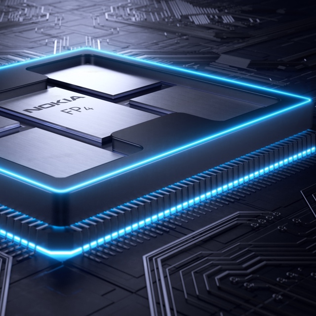 Nokia's FP4 p-chip. The multi-chip module shows five packages: the p-chip die surrounded by four memory stacks. Each stack has five memory die. The p-chip and memory stacks are interconnected using an interposer.
 - Nokia has unveiled the FP4, a 2.4 terabit-per-second network processor that has 6x the throughput of its existing FP3.
- The FP4 is a four-IC chipset implemented using 16nm CMOS FinFET technology. Two of the four devices in the chipset are multi-chip modules.
- The FP4 uses 56 gigabit-per-second serial-deserialiser (serdes) technology from Broadcom, implemented using PAM-4 modulation. It also supports terabit flows.
- Nokia announced IP edge and core router platforms that will use the FP4, the largest configuration being a 0.58 petabit switching capacity router.
Much can happen in an internet minute. In that time, 4.1 million YouTube videos are viewed, compared to 2.8 million views a minute only last year. Meanwhile, new internet uses continue to emerge. Take voice-activated devices, for example. Amazon ships 50 of its Echo devices every minute, almost one a second.
Given all that happens each minute, predicting where the internet will be in a decade’s time is challenging. But that is the task Alcatel-Lucent’s (now Nokia’s) chip designers set themselves in 2011 after the launch of its FP3 network processor chipset that powers its IP-router platforms.
Six years on and its successor - the FP4 - has just been announced. The FP4 is the industry’s first multi-terabit network processor that will be the mainstay of Nokia’s IP router platforms for years to come.
Cloud-scale routing
At the FP4’s launch, Nokia’s CEO, Rajeev Suri, discussed the ‘next chapter’ of the internet that includes smart cities, new higher-definition video formats and the growing number of connected devices.
IP traffic is growing at a compound annual growth rate (CAGR) of 25 percent through to 2022, according to Nokia Bell Labs, while peak data rates are growing at a 39 percent CAGR. Nokia Bell Labs also forecasts that the number of connected devices will grow from 12 billion this year to 100 billion by 2025.
Basil Alwan, Nokia’s president of IP and optical networks, said the internet has entered the era of cloud-scale routeing. When delivering a cloud service, rarely is the request fulfilled by one data centre. Rather, several data centres are involved in fulfilling the tasks. “One transaction to the cloud is multiplied,” said Alwan.
IP traffic is also becoming more dynamic, while the Internet of Things presents a massive security challenge.
Alwan also mentioned how internet content providers have much greater visibility into their traffic whereas the telcos’ view of what flows in their networks is limited. Hence their interest in analytics to understand and manage their networks better.
These are the trends that influenced the design of the FP4.
We put a big emphasis on making sure we had a high degree of telemetry coming out at the chip level
FP4 goals
Telemetry, the sending of measurement data for monitoring purposes, and network security were two key design goals for the FP4.
 Steve Vogelsang“We put a big emphasis on making sure we had a high degree of telemetry coming out at the chip level,” said Steve Vogelsang, CTO for Nokia's IP and optical business.
Tasks include counters, collecting statistics and packet copying. “This is to make sure we have the instrumentation coming off these systems that we can use to drive the [network] analytics platform,” said Vogelsang.
Being able to see the applications flowing in the network benefits security. Distributed Denial-of-Service (DDoS) attacks are handled by diverting traffic to a ‘scrubbing centre’ where sophisticated equipment separates legitimate IP packets from attack traffic that needs scrubbing.
The FP4 supports the deeper inspection of packets. “Once we identify a threat, we can scrub that traffic directly in the network,” said Vogelsang. Nokia claims that that the FP4 can deal with over 90 percent of the traffic that would normally go to a scrubbing centre.
Chipset architecture
Nokia’s current FP3 network processor chipset comprises three devices: the p-chip network processor, the q-chip traffic manager and the t-chip fabric interface device.
The p-chip network processor inspects packets and performs table look-ups using fast-access memory to determine where packets should be forwarded. The q-chip is the traffic manager that oversees the packet flows and decides how packets should be dealt with, especially when congestion occurs. The third FP3 chip is the t-chip that interfaces to the router fabric.
The FP4 retains the three chips and adds a fourth: the e-chip - a media access controller (MAC) that parcels data from the router’s client-side pluggable optical modules for the p-chip. However, while the FP4 retains the same nomenclature for the chips as the FP3, the CMOS process, chip architecture and packaging used to implement the FP4 are significantly more advanced.
The FP4 can deal with over 90 percent of the traffic that would normally go to a scrubbing centre
Nokia is not providing much detail regarding FP4 chipset's architecture, unlike the launch of the FP3. “We wanted to focus on the re-architecture we have gone through,” said Vogelsang. But looking at the FP3 design, insight can be gained as to how the FP4 has likely changed.
The FP3’s p-chip uses 288 programmable cores. Each programmable core can process two instructions each clock cycle and is clocked at 1GHz.
The 288 cores are arranged as a 32-row-by-9-column array. Each row of cores can be viewed as a packet-processing pipeline. A row pipeline can also be segmented to perform independent tasks. The array’s columns are associated with table look-ups. The resulting FP3 p-chip is a 400-gigabit network processor.
Vogelsang said there is limited scope to increase the clock speed of the FP4 p-chip beyond 1GHz. Accordingly, the bulk of the FP4’s sixfold throughput improvement is the result of a combination of programmable core enhancements, possible a larger core array and, most importantly, system improvements. In particular, the memory architecture is now packaged within the p-chip for fast look-ups, while the chipset’s input-output lanes have been boosted from 10 gigabits-per-second (Gbps) to 50Gbps.
Nokia has sought to reuse as much of the existing microcode to program the cores for the FP4 p-chip but has added new instructions to take advantage of changes in the pipeline.
Software compatibility already exists at the router operating system level. The same SROS router operating system runs on Nokia’s network processors, merchant hardware from the like of Broadcom and on x86 instruction-set microprocessors in servers using virtualisation technology.
Such compatibility is achieved using a hardware abstraction layer that sits between the operating system and the underlying hardware. “The majority of the software we write has no idea what the underlying hardware is,” said Vogelsang.
Nokia has a small team of software engineers focussed on the FP4’s microcode changes but, due to the hardware abstraction layer, such changes are transparent to the main software developers.
The FP3’s traffic manager, the q-chip, comprises four reduced instruction set computer (RISC) cores clocked at 900MHz. This too has been scaled up for the FP4 but Nokia has not given details.
The t-chip interfaces to the switch fabric that sits on a separate card. In previous generations of router products, a mid-plane is used, said Nokia. This has been scrapped with the new router products being announced. Instead, the switch cards are held horizontally in the chassis and the line cards are vertical. “A bunch of metal guides are used to guide the two cards and they directly connect to each other,” said Vogelsang. “The t-chips are what interface to these connectors inside the system.”
The MAC e-chip interfaces to the line card’s pluggable modules and support up to a terabit flow. Indeed, the MAC will support integer multiples of 100 Gigabit Ethernet from 100 gigabit to 1 terabit. Nokia has a pre-standard implementation of FlexMAC that allows it to combine lanes across multiple transceivers into a single interface.
Nokia will have line cards that support 24 or 36 QSFP-DD pluggable modules, with each module able to support 400 Gigabit Ethernet.
The FP4 is also twice as power efficient, consuming 4 gigabit/W.
We wanted to make sure we used a high-volume chip-packaging technology that was being driven by other industries and we found that in the gaming industry
Design choices
One significance difference between the two network processor generations is the CMOS process used. Nokia skipped 28nm and 22nm CMOS nodes to go from 40nm CMOS for the FP3 to 16nm FinFET for the FP4. “We looked at that and we did not see all the technologies we would need coming together to get the step-function in performance that we wanted,” said Vogelsang.
Nokia also designed its own memory for the FP4.
“A challenge we face with each generation of network processor is finding memories and memory suppliers that can offer the performance we need,” said Vogelsang. The memory Nokia designed is described as intelligent: instructions can effectively be implemented during memory access and the memory can be allocated to do different types of look-up and buffering, depending on requirements.
Another key area associated with maximising the performance of the memory is the packaging. Nokia has adopted multi-chip module technology for the p-chip and the q-chip.
“We wanted to make sure we used a high-volume chip-packaging technology that was being driven by other industries and we found that in the gaming industry,” said Vogelsang, pointing out that the graphics processing unit (GPU) has similar requirements to those of a network processor. GPUs are highly memory intensive while manipulating bits on a screen is similar to manipulating headers and packets.
The resulting 2.5D packaged p-chip comprises the packet processor die and stacks of memory. Each memory stack comprises 5 memory die. All sit on an interposer substrate - itself a die that is used for dense interconnect of devices. The resulting FP4 p-chip is thus a 22-die multi-chip module.
“Our memory stacks are connected at the die edges and do not use through-silicon vias,” said Vogelsang. “Hence it is technically a 2.5D package [rather than 3D].”
The q-chip is also implemented as a multi-chip module containing RISC processors and buffering memory, whereas the router fabric t-chip and MAC e-chip are single-die ICs.
The FP4’s more advanced CMOS process also enables significantly faster interfaces. The FP4 uses PAM-4 modulation to implement 56Gbps interfaces. “You really need to run those bit rates much much higher to get the traffic into and out of the chip,” said Vogelsang.
Nokia says it is using embedded serialiser-deserialiser interface technology from Broadcom.
Next-gen routers
Nokia has also detailed the IP edge and core routers that will use the FP4 network processor.
The 7750 Service Router (SR-s) edge router family will support up to 144 terabits in a single shelf. This highest capacity configuration is the 7750 SR-14. It is a 24-rack-unit-plus-the-power-supply high chassis and supports a dozen line cards, each 12Tbps when using 100-gigabit modules, or 24x400GbE when using QSFP-DD modules.
Another new platform is the huge 7950 Extensible Routing System (XRS-XC) IP core router which can be scaled to 576 terabits - over half a petabit - when used in a six-chassis configuration. Combining the six chassis does not make require the use of front-panel client-side interfaces. Instead, dedicated interfaces are used with active optical cables to interlink the chassis.
The first router products will be shipped to customers at the year end with general availability expected from the first quarter of 2018.
Telefonica tests XGS-PON
Part 1: XGS and TWDM passive optical networks
Telefonica is the latest operator to test XGS-PON, the 10-gigabit passive optical networking standard.
“Operators want to show they are taking the maximum from their fibre investment,” says Ana Pesovic, marketing manager for fibre at Nokia, the supplier of the XGS-PON equipment used for the operator’s lab tests. “Telefonica has been really aggressive in their fibre deployments in the last couple of years.”
 Ana Pesovic
XGS-PON
Approved by the ITU-T in 2016, XGS-PON supports two rates: 10-gigabit symmetrical and the asymmetrical rate of 10 gigabits downstream (to the user) and 2.5 gigabits upstream.
XGS-PON has largely superseded the earlier XG-PON standard which supports the 10-gigabit asymmetrical rate only. “It is fair to say there is no traction for XG-PON,” says Pesovic. “Even in China [an early adopter of XG-PON], we see the interest slowly moving to XGS-PON.”
Nokia says it has now been involved in 40 XGS-PON trials and nine customers have deployed the technology. “These have just started and they are not massive deployments,” says Pesovic.
Nokia’s XGS-PON customers include China Telecom and SK Broadband. SK Broadband has deployed XGS-PON alongside the more advanced TWDM-PON (time wavelength division multiplexing, passive optical network), the ITU-T NG-PON2 standard.
XGS-PON uses a fixed wavelength to deliver either the 10-gigabit symmetrical or asymmetrical service. The standard supports a distance of 20km and a split ratio of up to 1:128 - one XGS-PON optical line terminal (OLT) serving up to 128 optical network units (ONUs). In contrast, TWDM-PON supports four wavelengths enabling up to 40-gigabit symmetrical rates. And unlike XGS-PON, TWDM-PON supports flexible wavelengths using tuneable lasers.
The wavelengths used by XGS-PON and TWDM-PON have been specified such that the two standards can operate alongside GPON on the same fibre. Accordingly, with SK Broadband’s deployment, the two PON standards along with GPON support an aggregate capacity of 52.5 gigabits-per-second.
As well as testing XGS-PON's performance, Telefonica has tested that XGS-PON works without disturbing existing broadband services over its GPON networks, says Pesovic.
For the test, Telefonica used an 8-port line card where each port can be configured for XGS-PON or as a wavelength of a TWDM-PON. The line card fits within Nokia’s 7360 Intelligent Services Access Manager (ISAM) FX platform.
5G will require the deployment of many more small cells. With XGS-PON, multiple small cells can be served using a single PON
Applications
XGS-PON with its symmetrical 10-gigabit rate is suited to business services. "Operators can use one network to converge business and residential; today they are two overlay networks,” says Pesovic. Many businesses require 1-gigabit connectivity or less but by having a 10-gigabit link, multiple enterprises can be aggregated on one PON.
Nokia says that in countries such as South Korea as well as in Europe and North America there is also interest in a 10-gigabit PON for residential services. “People are taking the downstream bandwidth for granted and now the upstream is becoming a differentiator, making the quality of experience much better,” says Pesovic.
The bulk of traffic is still predominately downstream but increasingly users want to upload large files and video. Even if these uploads are of shorter duration, the network must deliver, says Pesovic.
Operators are also eyeing XGS-PON for the emerging 5G cellular standard. Nokia points out that 5G will require the deployment of many more small cells. With XGS-PON, multiple small cells can be served using a single PON.
Nokia expects XGS-PON will be deployed for years to come. Broadband is advancing by adding more wavelengths. To GPON, which uses one wavelength, can be added a second wavelength supporting 10-gigabit XGS-PON. Using TWDM-PON adds four and potentially eight more wavelengths - 40 gigabits and 80 gigabits of bandwidth, respectively. “It really doesn’t matter what the technology is called,” says Pesovic.
One North American operator is looking at TWDM-PON as a way to save power. During the night when there is less broadband usage, the operator wants to use wavelength mobility to migrate users onto a single wavelength.
TWDM-PON
Besides wavelength count, TWDM-PON differs from XGS-PON in its use of tuneable lasers.
Having tuneable wavelengths delivers several benefits to the operators. One is load balancing. If users on one wavelength start to exhaust its capacity, several users can be moved to a second wavelength that is less heavily loaded.
TWDM-PON also benefits network sharing and wavelength unbundling. A third-party operator can offer its fibre to interested operators. “Each operator could then operate on a single wavelength,” says Pesovic. If a user changes operator, they can simply be moved from one wavelength to another.
There are also operational benefits. If a fault develops on a board, users can be migrated to a second card without service interruption and the faulty board replaced.
One North American operator is looking at TWDM-PON as a way to save power, says Pesovic. During the night when there is less broadband usage, the operator wants to use wavelength mobility to migrate users onto a single wavelength. This would deliver sufficient bandwidth to those users that are active while allowing the remaining wavelengths to be powered down, saving power.
The issue impeding the uptake of TWDM-PON remains the high cost of tuneable lasers. Nokia expects it to be at least another year before the cost of tuneable lasers becomes more economical for PON. That said, service providers delivering businesses services may still be tempted to adopt TWDM-PON despite the higher cost of tuneable lasers given that the average revenue per user (ARPU) of business users is 5x that of residential users, says Pesovic.
See Part 2: FSAN unveils roadmap plans, click here
Telefónica tackles video growth with IP-MPLS network
- Telefónica’s video growth in one year has matched nine years of IP traffic growth
- Optical mesh network in Barcelona will use CDC-ROADMs and 200-gigabit coherent line cards
Telefónica has started testing an optical mesh network in Barcelona, adding to its existing optical mesh deployment across Madrid. Both mesh networks are based on 200-gigabit optical channels and high-degree reconfigurable add-drop multiplexers (ROADMs) that are part of the optical infrastructure that underpins the operator’s nationwide IP-MPLS network that is now under construction.
 Maria Antonia CrespoThe operator decided to become a video telco company in late 2014 to support video-on-demand and over-the-top streaming video services.
Telefónica realised its existing IP and aggregation networks would not be able to accommodate the video traffic growth and started developing its IP-MPLS network.
“What we are seeing is that the traffic is growing very quickly,” says Maria Antonia Crespo, IP and optical networking director at Telefónica. “In one year we are getting the same
figures as we got from internet traffic in the last nine years.”
The operator is rolling out the IP-MPLS network across Spain. Juniper Networks and Nokia are the suppliers of the IP router equipment, while Huawei and Nokia were chosen to supply the optical networking equipment.
IP-MPLS
Telefónica set about reducing the number of layers and number of hops when designing its IP-MPLS network. “At each hop, we have to invest money if we want to increase capacity,” says Crespo.

The result is an IP-MPLS network comprising four layers (see diagram). The uppermost Layer 1, dubbed HL1, connects the network to the internet world, while HL2 is a backbone transit layer. The HL3 layer is also a transit layer but at the provincial level. Spain is made up of 52 provinces. HL4 is where the services will reside, where Telefonica will deliver such services as Layer 2 and Layer 3 virtual private networks.
Between HL1 and HL2 is a national GMPLS-based photonic mesh, says Crespo, and between HL3 and HL4 there are the metro mesh networks. “Now we are deploying two GMPLS-based mesh networks, in Madrid and Barcelona,” she says. “Then, in the rest of the country, we are deploying [optical] rings.”
Systems requirements
Telefónica says it had several requirements when choosing the optical transport equipment, requirements common to both its backbone and regional networks.
One is the need to scale capacity at 10 gigabits and 100 gigabits, while network availability and robustness are also key. Telefónica says its network is designed to withstand two or more simultaneous fibre failures. “We have long experience with the GMPLS control plane to support different fibre impairments in the network,” says Alberto Colomer, optical technology manager at Telefónica.
The operator also wants its equipment to support high-speed interfaces and more granular rates to allow it to transition away from legacy traffic such as SDH and 1GbE. Operational improvements are another requirement: Telefónica wants to reduce the manual intervention its network needs. Optical time-domain reflectometers (OTDR) are being integrated into the network to monitor the fibre, as is the ability to automatically equalise the different optical channels.
 Alberto ColomerLastly, Telefónica is looking to reduce its capital expenditure and operational expense. It is deploying flexible rate 200-gigabit transponders in its Barcelona and Madrid networks and the same line cards will support 400-gigabit and even 1 terabit channels in future, as well as flexible grid to support the most efficient use of a fibre’s spectrum.
The 200-gigabit transponders use 16-quadrature amplitude modulation (16-QAM). Such transponders have enough reach to span each of the two cities but Colomer says Telefónica is still studying how many ROADM stages the 16-QAM transponders can cross.
It is like a pilot changing the engines while flying a plane
The ROADMs Telefónica is deploying in Madrid are directionless and are able to support up to 20 degrees. “You need some connectivity inside the mesh but also the mesh has to be connected to rings that cover all the counties around Madrid,” says Colomer.
Barcelona will be the first location where the ROADMs will also be colourless and contentionless (CDC-ROADMs). “We need to understand in a better way what are the advantages that come with that functionality,” says Colomer.
Telefónica has deployed Huawei’s Optix OSN 9800 platform in Madrid while in Barcelona Nokia’s 1830 Photonic Service Switch with the latest PSE-2 Coherent DSP-ASIC technology is being deployed.
Nokia’s PSS-1830 is designed to support the L-band as well as the C-band but Telefonica does not see the need for the L-band in the near future. “We are going in the direction of increasing capacity per channel: 400-gigabit channels and one terabit channels,” says Colomer. By deploying a photonic mesh and high-degree ROADMs, it will also be possible to increase capacity on a specific link by adding a fibre pair.
Status
The mesh in Madrid is already completed while Telefónica is deploying optical rings around Barcelona while it tests the contentionless ROADMs. These deployments are aligned with the IP-MPLS deployment, says Crespo, which is expected to be completed by 2018.
Crespo says the nationwide IP-MPLS rollout is a challenge. The deployment involves learning new technology that needs to be deployed alongside its existing network. "My boss likens it to a pilot changing the engines while flying a plane," says Crespo. "We are testing in the labs, duplicating it [the network], and migrating the traffic without impacting the customer."
Nokia’s PSE-2s delivers 400 gigabit on a wavelength
Four hundred gigabit transmission over a single carrier is enabled using Nokia’s second-generation programmable Photonic Service Engine coherent processor, the PSE2, part of several upgrades to Nokia's flagship PSS 1830 family of packet-optical transport platforms.
 Kyle Hollasch“One thing that is clear is that performance will have a key role to play in optics for a long time to come, including distance, capacity per fiber, and density,” says Sterling Perrin, senior analyst at Heavy Reading.
This limits the appeal of the so-called “white box” trend for many applications in optics, he says: “We will continue to see proprietary advances that boost performance in specific ways and which gain market traction with operators as a result”.
The 1830 Photonic Service Switch
The 1830 PSS family comprises dense wavelength-division multiplexing (DWDM) platforms and packet-OTN (Optical Transport Network) switches.
The DWDM platform includes line amplifiers, reconfigurable optical add-drop multiplexers (ROADMs), transponder and muxponder cards. The 1830 platforms span the PSS-4, -8, -16 and the largest and original -32, while the 1830 PSS packet-OTN switches include the PSS-36 and the PSS-64 platforms. The switches include their own coherent uplinks but can be linked to the 1830 DWDM platforms for their line amps and ROADMs.
The 1830 PSS upgrades include a 500-gigabit muxponder card for the DWDM platforms that feature the PSE2, new ROADM and line amplifiers that will support the L-band alongside the C-band to double fibre capacity, and the PSS-24x that complements the two existing OTN switch platforms.
100-gigabit as a service
In DWDM transmissions, 100-gigabit wavelengths are commonly used to transport multiplexed 10-gigabit signals. Nokia says it is now seeing increasing demand to transport 100-gigabit client signals.
“One hundred gigabit is becoming the new currency,” says Kyle Hollasch, director, optical marketing at Nokia. “No longer is the thinking of 100 gigabit just as a DWDM line rate but 100 gigabit as a service, being handed from a customer for transport over the network.”
Current PSS 1830 platform line cards support 50-gigabit, 100-gigabit and 200-gigabit coherent transmission using polarisation-multiplexed, binary phase-shift keying (PM-BPSK), quadrature phase-shift keying (PM-QPSK) and 16 quadrature amplitude modulation (PM-16QAM), respectively. Nokia now offers a 500-gigabit muxponder card that aggregates and transports 100-gigabit client signals. The 500-gigabit muxponder card has been available since the first quarter and already several hundred cards have been shipped.
“The challenge is not just to crank up capacity but to do so profitably,” says Hollasch. “Keeping the cost-per-bit down, the power consumption down while pushing towards the Shannon limit [of fibre] to carry more capacity.”
 Source: Nokia
Modulation formats
The PSE2 family of coherent processors comprises two designs: the high-end super-coherent PSE-2s and the compact low-power PSE-2c.
Nokia joins the likes of Ciena and Infinera in developing several coherent ASICs, highlighting how optical transport requirements are best met using custom silicon. Infinera also announced its latest generation photonic integrated circuit that supports up to 2.4 terabits.
The high-end PSE-2s is a significant enhancement on the PSE coherent chipset first announced in 2012. Implemented using 28nm CMOS, the PSE-2s has a power consumption similar to the original PSE yet halves the power consumption-per-bit given its higher throughput.
The PSE-2s adds four modulation formats to the PSE’s existing three and supports two symbol rates: 32.5 gigabaud and 44.5 gigabaud. The modulation schemes and distances they enable are shown in the chart.

The 1.4 billion transistor PSE-2s has sufficient processing performance to support two coherent channels. Each channel can implement a different modulation format if desired, or the two can be tightly coupled to form a super-channel. The only exception is the 400-gigabit single wavelength format. Here the PSE-2s supports only one channel implemented using a 45 gigabaud symbol rate and PM-64QAM. The 400-gigabit wavelength has a relatively short 100-150km reach, but this suits data centre interconnect applications where links are short and maximising capacity is key.
Nokia recently conducted a lab experiment resulting in the sending of 31.2 terabits of data over 90km of standard single-mode fibre using 78, 400-gigabit channels spaced 50GHz apart across the C-band. "We were only limited by the available hardware from reaching 35 terabits," says Hollasch.
Using the 45-gigabaud rate and PM-16QAM enables two 250-gigabit channels. This is how the 500-gigabit muxponder card is achieved. The 250-gigabit wavelength has a reach of 900km, and this can be extended to 1,000km but at 200 gigabit by dropping to the 32-gigabaud symbol rate, as implemented with the current PSE chipset.
Nokia also offers 200 gigabit implemented using 45 gigabaud and 8-QAM. “The extra baud rate gets us [from 150 gigabit] to 200 gigabit; this is very valuable,” says Hollasch. The resulting reach is 2,000km and he expects this format to gain the most market traction.
The PSE-2s, like the PSE, also implements PM-QPSK and PM-BPSK but with reaches of 3,000-5,000km and 10,000km, respectively.
The PSE-2s introduces a fourth modulation format dubbed set-partition QPSK (SP-QPSK).
Standard QPSK uses amplitude and phase modulation resulting in a 4-point constellation. With SP-QPSK, only three out of the possible four constellation points are used for any given symbol. The downside of the approach is that a third fewer constellation points are used and hence less data is transported but the lost third can be restored using the higher 45-gigabaud symbol rate.
The benefit of SP-QPSK is its extended reach. “By properly mapping the sequence of symbols in time, you create a greater Euclidean distance between the symbol points,” says Hollasch. “What that gives you is gain.” This 2.5dB extra gain compared to PM-QPSK equates to a reach beyond 5,000km. “That is the territory most implementation are using BPSK and also addresses a lot of sub-sea applications,” says Hollasch. “Using SP-QPSK [at 100 gigabit] also means fewer carriers and hence, it is more spectrally efficient than [50-gigabit] BPSK.”
The PSE-2c
The second coherent DSP-ASIC in the new family is the PSE-2c compact, also implemented in 28nm CMOS, designed for smaller, low-power metro platforms and metro-regional reaches.
The PSE-2c supports a 100-gigabit line rate using PM-QPSK and will be used alongside the CFP2-ACO line-side pluggable module. The PSE-2c consumes a third of the power of the current PSE operating at 100 gigabit.
“We are putting the PSE2 [processors] in multiple form factors and multiple products,” says Hollasch.
The recent Infinera and Nokia announcements highlight the electronic processing versus photonic integration innovation dynamics, says Heavy Reading's Perrin. He notes how innovations in electronics are driving transmission across greater distances and greater capacities per fibre and finding applications in both long haul and metro networks as a result.
“Parallel photonic integration is a density play, but even Infinera’s ICE announcement is a combination of photonic integration and electronic processing advancements,” says Perrin. “In our view, electronic processing has taken a front seat in importance for addressing fibre capacity and transmission distance, which is why the need for parallel photonic integration in transport has not really spread beyond Infinera so far.”
 The PSS-24x showing the 24, 400 gigabit line cards and 3 switch fabric cards, 2 that are used and one for redundancy. Source: Nokia
PSS-24x OTN switch
Nokia has also unveiled its latest 28nm CMOS Transport Switch Engine, a 2.4-terabit non-blocking OTN switch chip that is central to its latest PSS-24x switch platform. Two such chips are used on a fabric card to achieve 4.8 terabits, and three such cards are used in the PSS-24x, two active cards and a third for redundancy. The result is 9.6 terabits of switching capacity instead of the current platforms' 4 terabits, while power consumption is halved.
Nokia says it already has a roadmap to 48-terabits of switching capacity. “The current generation [24x] shipping in just a few months is 400-gigabit per slot,” says Hollasch. The 24 slots that fit within the half chassis results in 9.6 terabits of switching capacity. However, Nokia's platform roadmap will achieve 1 terabit-per-slot by 2018-19. The backplane is already designed to support such higher speeds, says Hollasch. This would enable 24 terabits of switching capacity per shelf and with two shelves in a bay, a total switching capacity of 48 terabits.
The transport switch engine chip switches OTN only. It is not designed as a packet and OTN switch. “A cell-based agnostic switching architecture comes with a power and density penalty,” explains Hollasch, adding that customers prefer the lowest possible power consumption and highest possible density.
The result is a centralised OTN switch fabric with line-card packet switching. Nokia will introduce packet switching line cards next year that will support 300 gigabit per card. Two such cards will be ‘pair-able’ to boost capacity to 600 gigabit but Hollasch stresses that the PSS-24x will not switch packets through its central fabric.
Doubling capacity with the L-band
By extending the 1830 PSS platform to include the L-band, up to 70 terabits of data can be supported on a fibre, says Hollasch.
Nokia has developed a line card that supports both C-band and L-band amplification that will be available around the fourth quarter of this year. The ROADM and 500-gigabit muxponder card for the L-band will be launched in 2017.
Once the amplification is available, operators can start future-proofing their networks. Then when the L-band ROADMs and muxponder cards become available, operators can pay as they grow; extending wavelengths into the L-band, once all 96 channels of the C-band are used, says Hollasch.