
OFC 2024 reflects a mature industry with new offshoots
- The three General Chairs preview the upcoming Optical Fiber Communications (OFC) conference and discuss photonics developments and trends.
- The General Chairs' role is to choose the plenary speakers, programme theme, and conference schedule.
- OFC takes place during March 24th-28th in San Diego, CA.*
Photonics, at least for traditional applications, has become a mature industry. So says Professor Dimitra Simeonidou, one of this year’s OFC General Chairs.
y traditional, Simeonidou is referring to classical optical communications.
But she also stresses new developments: the use of optical fibres for environmental sensing, optics for satellites, and quantum.
“Quantum is like a micro-OFC,” says Simeonidou. “You have issues from technology to subsystem to system applications now appearing in the OFC programmes.”

The OIF's coherent optics work gets a ZR+ rating
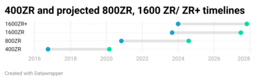
The OIF has started work on a 1600ZR+ standard to enable the sending of 1.6 terabits of data across hundreds of kilometres of optical fibre.The initiative follows the OIF's announcement last September that it had kicked off 1600ZR. ZR refers to an extended reach standard, sending 1.6 terabits over an 80-120km point-to-point link.
600ZR follows the OIF’s previous work standardising the 400-gigabit 400ZR and the 800-gigabit 800ZR coherent pluggable optics.
The decision to address a ‘ZR+’ standard is a first for the OIF. Until now, only the OpenZR+ Multi-Source Agreement (MSA) and the OpenROADM MSA developed interoperable ZR+ optics.
The OIF’s members’ decision to back the 1600ZR+ coherent modem work was straightforward, says Karl Gass, optical vice chair of the OIF’s physical link layer (PLL) working group. Several companies wanted it, and there was sufficient backing. “One hyperscaler in particular said: ‘We really need that solution’,” says Gass.
OIF, OpenZR+, and OpenROADM
Developing a 1600ZR+ standard will interest telecom operators who, like with 400ZR and the advent of 800ZR, can take advantage of large volumes of coherent pluggables driven by hyperscaler demand. However, Gass says no telecom operator is participating in the OIF 1600ZR+ work.
“It appears that they are happy with whatever the result [of the ZR+ work] will be,” says Gass. Telecom operators are active in the OpenROADM MSA.
Now that the OIF has joined OpenZR+ and the OpenROADM MSA in developing ZR+ designs, opinions differ on whether the industry needs all three.
“There is significant overlap between the membership of the OpenZR+ MSA and the OIF, and the two groups have always maintained positive collaboration,” says Tom Williams, director of technical marketing at Acacia, a leading member of the OpenZR+. “We view the adoption of 1600ZR+ in the OIF as a reinforcement of the value that the OpenZR+ has brought to the market.”
Robert Maher, Infinera’s CTO, believes the industry does not need three standards. However, having three organisations does provide different perspectives and considerations.
Meanwhile, Maxim Kuschnerov, director R&D at Huawei, says the OIF’s decision to tackle ZR+ changes things.”OpenZR+ kickstarted the additional use cases in the industry, and OpenROADM took it away but going forward, it doesn’t seem that we need additional MSAs if the OIF is covering ZR+ for Ethernet clients in ROADM networks,” says Kuschnerov. “Only the OTN [framing] modes need to be covered, and the ITU-T can do that.”
Kuschnerov also would like more end-user involvement in the OIF group. “It would help shape the evolving use cases and not be guided by a single cloud operator,” he says.
ZR history
The OIF is a 25-year-old industry organisation with over 150 members, including hyperscalers, telecom operators, systems and test equipment vendors, and component companies.
In October 2016, the OIF started the 400ZR project, the first pluggable 400-gigabit Ethernet coherent optics specification. The principal backers of the 400ZR work were Google and Microsoft. The standard was designed to link equipment in data centres up to 120km apart.
The OIF 400ZR specification also included an un-amplified version with a reach of several tens of kilometres. The first 400ZR specification document, which the OIF calls an Implementation Agreement, was completed in March 2020 (see chart above).
The OIF started the follow-up on the 800ZR specification in November 2020, a development promoted by Google. Gass says the OIF is nearing completion of the 800ZR Implementation Agreement document, expected in the second half of 2024.
If the 1600ZR and ZR+ coherent work projects take a similar duration, the first 1600ZR and 1600ZR+ products will appear in 2027.
Symbol rate and other challenges
Moving to a 1.6-terabit coherent pluggable module using the same modulation scheme – 16-ary quadrature amplitude modulation or 16-QAM – used for 400ZR and 800ZR suggests a symbol rate of 240 gigabaud (GBd).
“That is the maths, but there might be concerns with technical feasibility,” says Gass. “That’s not to say it won’t come together.”
The highest symbol rate coherent modem to date is Ciena’s WaveLogic 6e, which was announced a year ago. The design uses a 3nm CMOS coherent digital signal processor (DSP) and a 200GBd symbol rate. It is also an embedded coherent design, not one required to fit inside a pluggable optical module with a constrained power consumption.
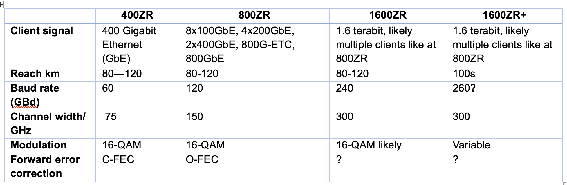
Kuschnerov points out that the baud rates of ZR and ZR+ have differed. And this will likely continue. 800ZR, using Ethernet with no probabilistic constellation shaping, has a baud rate of 118.2GBd, while 800ZR+, which uses OTN and probabilistic constellation shaping, has a baud rate of up to 131.35GBd. Every symbol has a varying probability when probabilistic constellation shaping is used. “This decreases the information per symbol, and thus, the baud rate must be increased,“ says Kuschnerov.
Doubling up for 1600ZR/ ZR+, those numbers become around 236GBd and 262GBd, subject to future standardisation. “So, saying that 1600ZR is likely to be at 240GBd is correct, but one cannot state the same for a potential 1600ZR+,” says Kuschnerov.
Nokia’s view is that for 1600ZR, the industry will look at operating modes that include 16QAM at 240 GBd. Other explored options include 64-QAM with probabilistic constellation shaping at 200GBd and even dual optical carrier solutions with each carrier operating at approximately 130GBd. “However, this last option may be challenging from a power envelope perspective,” says Szilárd Zsigmond, head of Nokia’s optical subsystems group.
In turn, if 1600ZR+ reaches 1,000km distances, the emphasis will be on higher baud rate options than those used for 1600ZR. “This will be needed to enable longer reaches, which will also put pressure on managing power dissipation,” says Zsigmond.
The coherent DSP must also have digital-to-analogue (DACs) and analogue-to-digital converters (ADCs) to sample at least at 240 giga-samples per second. Indeed, the consensus among the players is that achieving the required electronics and optics will be challenging.
“All component bandwidths have to double and that is a significant challenge,” says Josef Berger, associate vice president, cloud optics marketing at Marvell.
The coherent optics – the modulators and receivers – must extend their analogue bandwidth of 120GHz. Infinera is one company that is confident this will be achieved. “Infinera, with our highly integrated Indium Phosphide-based photonic integrated circuits, will be producing a TROSA [transmitter-receiver optical sub-assembly] capable of supporting 1.6-terabit transmission that will fit in a pluggable form factor,” says Maher.
The coherent DSP and optics operating must also meet the pluggable modules’ power and heat limits. “That is an extra challenge here: the development needs to maintain focus on cost and power simultaneously to bring the value network operators need,” says Williams. “Scaling baud rate by itself doesn’t solve the challenge. We need to do this in a cost and power-efficient way.”
Current 800ZR modules consume 30W or more, and since the aim of ZR modules is to be used within Ethernet switches and routers, this is challenging. In comparison, 400ZR modules now consume 20W or less.
“For 800ZR and 800ZR+, the target is to be within the 28W range, and this target is not changing for 1600ZR and 1600ZR+,” says Zsigmond. Coherent design engineers are being asked to double the bit rate yet keep the power envelope constant.
Certain OIF members are also interested in backward compatibility with 800ZR or 400ZR. “That also might affect the design,” says Gass.
Given the rising cost to tape out a coherent DSP using 3nm and even 2nm CMOS process nodes required to reduce power per bit, most companies designing ASICs will look to develop one design for the 1600ZR and ZR+ applications to maximise their return on investment, says Zsigmond, who notes that the risk was lower for the first generations of ZR and ZR+ applications. Most companies had already developed components for long-haul applications that could be optimised for ZR and ZR+ applications.
For 400ZR, which used a symbol rate of 60 GBd, 60-70 GBd optics already existed. For 800 gigabit transmissions, high-performance embedded coherent optics and pluggable, low-power ZR/ZR+ modules have been developed in parallel. “For 1600ZR/ZR+, it appears that the pluggable modules will be developed first,” says Zsigmond. “There will be more technology challenges to address than previous ZR/ZR+ projects.”
The pace of innovation is faster than traditional coherent transmission systems and will continue to reduce cost and power per bit, notes Marvell’s Berger: “This innovation creates technologies that will migrate into traditional coherent applications as well.”
Gass is optimistic despite the challenges ahead: “You’ve got smart people in the room, and they want this to happen.”
OIF's OFC 2024 demo
The OIF has yet to finalise what it will show for the upcoming coherent pluggable module interoperable event at OFC to be held in San Diego in March. But there will likely be 400ZR and 800ZR demonstrations operating over 75km-plus spans and 400-gigabit OpenZR+ optics operating over greater distance spans.
Optical transmission: sending more data over a greater reach
Keysight Technologies' chart plots the record-setting optical transmission systems of recent years.
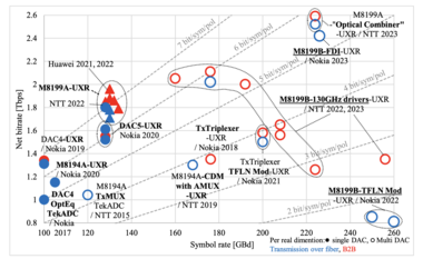
The chart, compiled by Dr Fabio Pittalá, product planner, broadband and photonic center of excellence at Keysight, is an update of one previously published by Gazettabyte.
The latest chart adds data from last year’s conferences at OFC 2023 and ECOC 2023. And new optical transmission achievements can be expected at the upcoming OFC 2024 show, to be held in San Diego, CA in March.

Working at the limit of optical transmission performance

- Expect to see new optical transmission records at the upcoming ECOC 2023 conference.
- Keysight Technologies’ chart plots the record-setting optical transmission systems of recent years.
- The chart reveals optical transmission performance issues and the importance of the high-speed converters between the analogue and digital domains for test equipment and, by implication, for coherent digital signal processors (DSPs).
Engineers keep advancing optical systems to send more data across an optical fibre.
It requires advances in optical and electronic components that can process faster, higher-bandwidth signals, and that includes the most essential electronics part of all: the coherent DSP chip.
Coherent DSPs use state-of-the-art 5nm and 3nm CMOS chip manufacturing processes. The chips support symbol rates from 130-200 gigabaud (GBd). At 200GBd, the coherent DSP’s digital-to-analogue converters (DACs) and analogue-to-digital converters (ADCs) must operate at at least 200 giga samples-per-second (GSps) and likely closer to 250GSps. DACs drive the optical modulator in the optical transmission path while the ADCs are used at the optical receiver to recover the signal.
Spare a thought for the makers of test equipment used in labs that drive such coherent optical transmission systems. The designers must push their equipments’ DACs and ADCs to the limit to generate and sample the waveforms of these prototype next-generation optical transmission systems.
Optical transmission records
The recent history of record-setting optical transmission systems reveals the design challenges of coherent components and how ADC and DAC designs are evolving.
It is helpful to see how test equipment designers tackle ADC and DAC design, given the devices are a critical element of the coherent DSP, and when vendors are reluctant to detail how they achieve 200GBd baud rates using on-chip CMOS-based ADCs and DACs.
Nokia and Keysight Technologies published a post-deadline paper at the ECOC 2022 conference detailing the transmission of a 260GBd single-wavelength signal over 100km of fibre.
The system achieved the high baud rate using a thin-film lithium niobate modulator driven by Keysight’s M8199B arbitrary waveform generator. The M8199B uses a design consisting of two interleaved DACs to generate signals at 260GSps.
A second post-deadline ECOC 2022 paper, published by NTT, detailed the sending of over two terabits-per-second (Tbps) on a single wavelength. This, too, used Keysight’s M8199B arbitrary waveform generator.
The chart above highlights optical transmission records since 2015, plotting the systems’ net bit rate – from 800 gigabits to 2.2 Tbps – against a symbol rate measured in GBd.
As with commercial coherent optical transport systems, the goal is to keep increasing the symbol rate. A higher symbol rate sends more data over the same fibre spans. For example, the 400ZR coherent transmission standard uses a symbol rate of some 60GBd to send a 400Gbps wavelength, while 800ZR doubles the baud rate to some 120GBd to transmit 800Gbps over similar distances.
“With the 1600ZR project just started by the OIF, this trend will likely continue,” says Fabio Pittalá, product planner, broadband and photonic center of excellence at Keysight.
The signal generator test equipment options include the use of different materials – CMOS and silicon germanium – and moving from one DAC to a parallel multiplexed DAC design.
Single DACs
In 2017, Nokia achieved a 1Tbps transmission using a 100GBd symbol rate. Nokia used a Micram 6-bit 100GSps DAC in silicon germanium for the modulation.
For its next advancement in transmission performance, in 2019, Nokia used the same DAC but a faster ADC at the receiver, moving from a Tektronix instrument using a 70GHz ADC to the Keysight UXR oscilloscope with a 110GHz bandwidth ADC. The resulting net bit rate was nearly 1.4 terabits.
Keysight also developed the M8194A arbitrary waveform generator based on a CMOS-based DAC. The higher sampling rate of this arbitrary waveform generator increased the baud rate to 105GBd, but because of the bandwidth limitation, the net bit rate was lower.
The bandwidth of CMOS DACs can be improved but it tops out in the region of 50-60GHz. “It’s very difficult to scale to a higher baud rate using this technology,” says Pittalá. Silicon germanium, by contrast, supports much higher bandwidths but has a higher power consumption.
In 2020, Nokia reached 1.6Tbps at 128GBd using the Micram DAC5, an 8-bit 128GSps DAC based on silicon germanium. A year later, Keysight released the M8199A arbitrary waveform generator. “This was also based on 8-bit silicon germanium DACs operating at 128GSps, but the signal-to-noise ratio was greatly improved, allowing to generate higher-order quadrature amplitude modulation formats with more than sixteen levels,” says Pittalá.
This arbitrary waveform generator was used in systems that, coupled with advanced equalisation schemes, pushed the net bit rate to almost 2Tbps.
Going parallel
For the subsequent advances in baud rate, parallel DAC designs, multiplexing two or more DACs together, were implemented by different research labs.
In 2015, NTT multiplexed two DACs that advanced the symbol rate from 105GBd to 120GBd. In 2019, NTT moved to a different type of multiplexer, which, used with the same DAC, increased the baud rate to around 170GBd. Nokia also demonstrated a multiplexed design concept, which, together with a novel thin-film lithium niobate modulator, extended the symbol rate to 200GBd, achieving a 1.6Tbps net bit rate.
Last year, Keysight introduced its latest arbitrary waveform generator, the M8199B. The design also adopted a multiplexed DAC design.
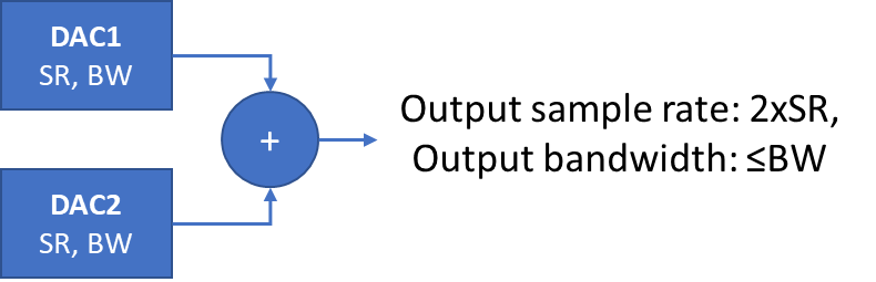
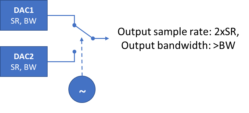
Multiplexing two DACs. SR refers to sample rate, BW refers to bandwidth. Source: Keysight.
“There are two 128GSps 8-bit silicon germanium DACs that are time-interleaved to get a higher speed signal per dimension,” says Pittalá. If the two DACs are shifted in time and added together, the result is a higher sampling rate overall. However, Pittalá points out that while the sample rate is effectively doubled, the overall bandwidth is defined by the individual DACs (see diagram above).
Pittalá also mentions another technique, based on active clocking, that does increase the bandwidth of the system. The multiplexer is clocked and acts like a fast switch between the two DAC channels. “In principle, you can double the bandwidth, ” he says. (See diagram below.)
The Keysight’s M8199B’s improved performance, combined with advances in components such as NTT’s 130GHz indium phosphide amplifier, resulted in over 2Tbps transmission, as detailed in the ECOC 2022 paper. As the baud rate was increased, the modulation scheme used and the net bit rate decreased. (Shown by the red dots on the chart).
In parallel, Keysight worked with Nokia, which used a thin-film lithium niobate modulator for their set-up, a different modulator to NTT’s. The test equipment directly drove the thin-film modulator; no external modulator driver was needed. The system was operated as high as 260GBd, achieving a net bit rate of 800Gbps.
Pittalà notes that while the NTT system differs from Nokia’s, Nokia’s two red points on the extreme right of the chart continue the trajectory of NTT’s six red points as the baud rate increases.
OFC’23 O-band record
The post-deadline papers at the OFC 2023 conference earlier this year did not improve the transmission performances of the ECOC papers.
A post-deadline paper published at OFC 2023 showed a record of coherent transmission in the O-Band. Working with Keysight, McGill University showed 1.6Tbps coherent transmission over 10km using a thin-film lithium niobate modulator. The system operated at 167GBd, used a 64-QAM modulation scheme, and used the Keysight M8199B.
Pittalà expects that at ECOC 2023, to be held in Glasgow in October, new record-breaking transmissions will be announced.
His chart will need updating.
Further information
Thin-film lithium niobate modulators, click here
Nokia jumps a class with its PSE-6s coherent modem
- The 130 gigabaud (GBd) PSE-6s coherent modem is Nokia’s first in-house design for high-end optical transport systems
- The PSE-6s can send an 800 gigabit Ethernet (800GbE) payload over 2,000km and 1.2 terabits of data over 100km.
- Two PSE-6s DSPs can send three 800GbE signals over two 1.2-terabit wavelengths
Nokia has unveiled its latest coherent modem, the super coherent Photonic Service Engine 6s (PSE-6s) that will power its optical transport platforms in the coming years.
The PSE-6s comes three years after Nokia announced its current generation of coherent digital signal processors (DSPs): the PSE-Vs DSP for the long-haul and the compact PSE-Vc for the coherent pluggable market.
Nokia is only detailing the PSE-6s; its next-generation coherent modem for pluggables will be a future announcement.
Nokia will demonstrate the PSE-6s at the upcoming OFC show in March while field trials involving systems using the PSE-6s will start in the year’s second half.
Reducing cost per bit
In 2020, Nokia bought Elenion, a silicon photonics company specialising in coherent optics.
The PSE-6s is Nokia’s first in-house coherent modem – the coherent DSP and associated optics – targeting the most demanding optical transport applications.
Nokia points out that coherent systems started approaching the Shannon limit two generations ago.
In the past, operators could reduce the cost of optical transport by sending more data down a fibre; upgrading the optical signal from 100 to 200 to 400 gigabit required only a 50GHz channel.
“You were getting more fibre capacity with each generation,” says Serge Melle, director of product marketing, optical networks at Nokia. And this helped the continual reduction of the cost-per-bit metric.
But with more advanced DSPs, implemented using 16nm, 7nm, and now 5nm CMOS, going to a higher symbol rate and hence data rate requires more spectrum, says Melle.
Increasing the symbol rate is still beneficial. It allows more data to be sent using the same modulation scheme or transmitting the same data payload over longer distances.
“So one of the things we are looking to do with the PSE-6s is how do we still enable a lower total cost of ownership even though you don’t get more capacity per wavelength or fibre,” says Melle.

Symbol rate classes
Coherent optics from the leading vendors use a symbol rate of 90-107 gigabaud (GBd), while Cisco-owned Acacia’s latest 1.2-terabit coherent modem in a CIM-8 module operates at 140GBd.
Acacia uses a classification system based on symbol rate. First-generation coherent systems operating at 30-34GBd are deemed Class 1. Class 2 doubles the baud rates to 60-68GBd, the symbol rate window used for 400ZR coherent optics, for hyperscalers to connect equipment across their data centres up to 120km apart.
The DSPs from the leading optical transport systems vendors operating at 90-107GBd are an intermediate step between Class 2 and Class 3 using Acacia’s classification. In contrast, Acacia has jumped directly from Class 2 to Class 3 with its 140GBd CIM-8 coherent modem.
Competitors view Acacia’s classification scheme as a marketing exercise and counter that their 90-107GBd optical transport systems benefited customers for over two years.
Nokia’s 90GBd PSE-Vs can send 400 gigabits using quadrature phase-shift keying (QPSK) over 3,000km. This contrasts with its earlier 67GBd PSE-3s that sends 400GbE up to 1,000km using 16-QAM.
However, with the PSE-Vs, Nokia, unlike its optical transport competitors, Infinera, Ciena and Huawei, decided not to support 800-gigabit wavelengths.
Nokia argued that 7nm CMOS, 90-100GBd coherent optics tops out at 600 gigabit when used for distances of several hundred kilometers, while metro-regional distances are more economically served using 400-gigabit pluggable optics such as the CFP2 implementing 400ZR+.
With the 130Gbd PSE-6s, Nokia has a Class 3 coherent modem with the PSE-6s capable of sending 800 gigabits more than 2,000km.
The PSE-6s also doubles the maximum data rate of the PSE-Vs to 1.2 terabits per wavelength. However, at 1.2 terabits, the reach is 100-plus km, valuable for very high capacity metro transport and data centre interconnect.
Scale, reach and power consumption per bit
Nokia highlights the PSE-6s’ main three performance metric improvements.
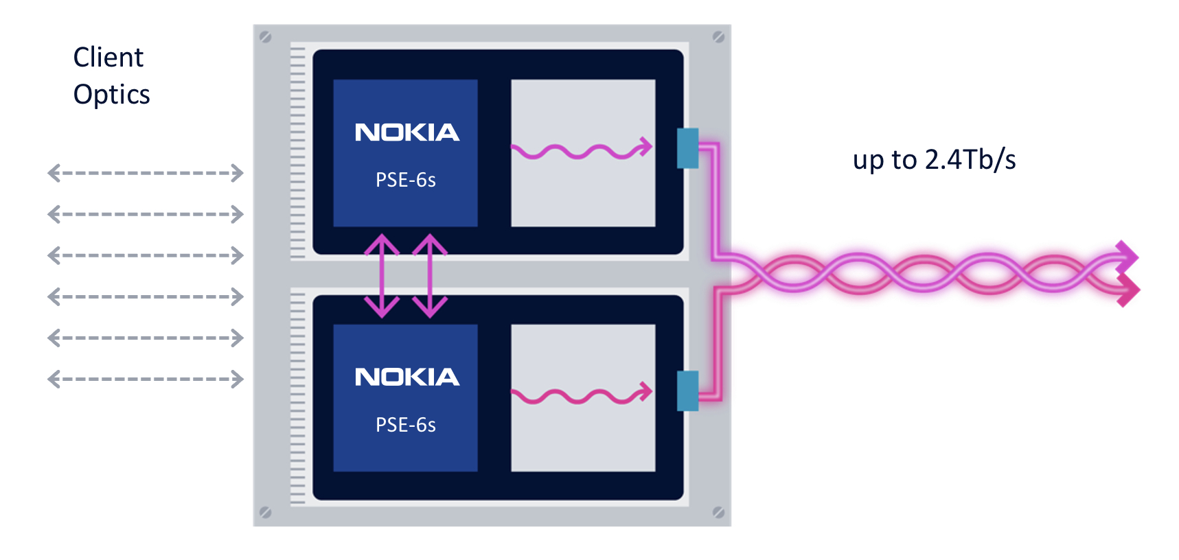
First, the coherent modem delivers scaling: two coherent optical engines fit on a line card to deliver 2.4 terabits to transport emerging high-speed services such as 800GbE.
The two PSE-6s are linked using a dedicated interface to share the client-side signals (see diagram).
“We are not the only ones introducing a 5nm solution, but I think we are the only ones that allow two DSPs to work together,” says Melle.
Without the interface, a single 800GbE and up to four 100GbE clients or a 400GbE client can be sent over each DSP’s 1.2-terabit wavelength. Adding the interface, an operator can send three uniform 800GbE clients, with the interface splitting the third 800GbE client between the two DSPs.
“In a single line card, you can stripe the three 800-gigabit services rather than have to deploy three separate line cards in the network,” says Melle.
Nokia is not detailing the interface used to link the DSPs but said that the interface is used for data only and not to share signal processing resources between the ASICs.
“There is an extra amount of circuitry to share the client bandwidth across the two DSPs, but it is not high power consuming, and most transponders have some circuitry between the clients and the DSP,” says Melle. “So the incremental ‘power tax’ is marginal; it doesn’t add any significant power overhead.”
The resulting 2.4-terabit transmission is sent as two 1.2-terabit wavelengths, each occupying a 150GHz-wide channel. Existing systems that operate at 90-107GBd typically use a 112.5GHz channel for an 800-gigabit transmission, so the PSE-6s delivers a fibre capacity benefit.
The two wavelengths can be bonded, as in a two-channel ‘super-channel’, or sent to separate locations.
The second improvement is optical performance. For example, an 800-gigabit payload can travel over 2,000km. Nokia claims this is 3x the reach of existing commercial optical transport systems.
The improved transmission performance is achieved using a combination of the 130GBd baud rate, probabilistic constellation shaping (PCS), and improved forward error correction (FEC). Melle says the contributions to the improvement are 90 per cent baud rate and 10 per cent due to coherent modem algorithm tweaks.
“Baud rate is king; that is what really drives this improved performance,” says Melle.
The third benefit is reduced power consumption at the device and system (networking) levels.
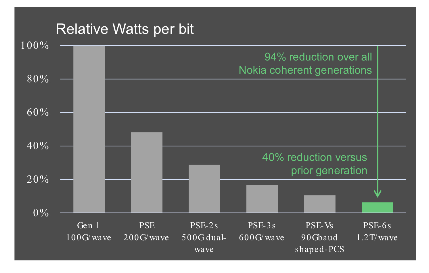
Using a 5nm finFET CMOS process to make the PSE-6s DSP ASIC and developing denser line cards (two modems per card) means systems will consume 60 per cent less power than Nokia’s existing coherent technology.
According to Nokia, the PSE-6s optical engine consumes 40 per cent fewer Watts per bit compared to the PSE-Vs.
Nokia 1830 transport systems
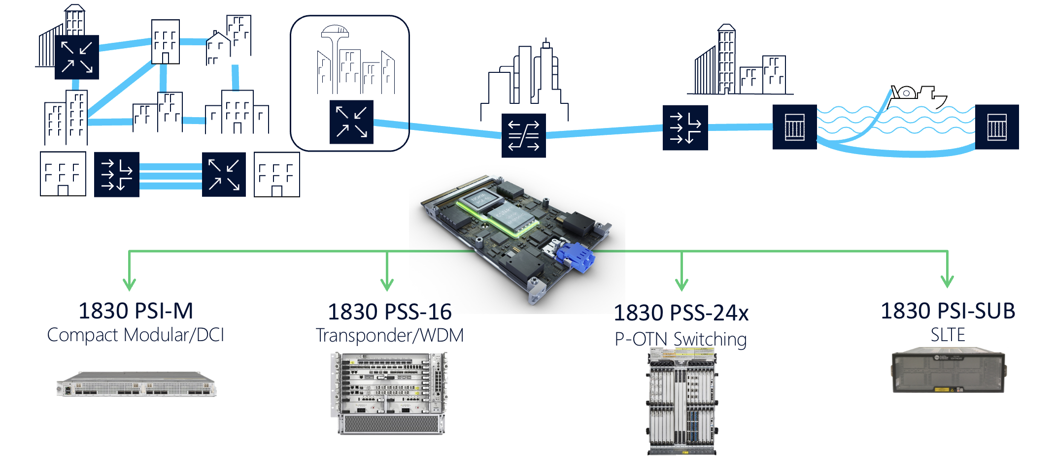
The PSE-6s line cards fit into Nokia’s existing range of 1830 transport platforms.
These include the 1830 PSI-M compact modular data centre interconnect, the 1830 PSS-16 transponder and WDM line system, the 1830 PSS-24x P-OTN and switching chassis, and the 1830 PSI-SUB subsea line-terminating equipment.
For example, the PSI-M platform can hold two line cards, each with two PSE-6s.

BT’s Open RAN trial: A mix of excitement and pragmatism

“We in telecoms, we don’t do complexity very well.” So says Neil McRae, BT’s managing director and chief architect.
He was talking about the trend of making network architectures open and in particular the Open Radio Access Network (Open RAN), an approach that BT is trialling.
“In networking, we are naturally sceptical because these networks are very important and every day become more important,” says McRae
Whether it is Open RAN or any other technology, it is key for BT to understand its aims and how it helps. “And most importantly, what it means for customers,” says McRae. “I would argue we don’t do enough of that in our industry.”
Open RAN
Open RAN has become a key focus in the development of 5G. Open RAN is backed by leading operators, it promises greater vendor choice and helps counter the dependency on the handful of key RAN vendors such as Nokia and Ericsson. There are also geopolitical considerations given that Huawei is no longer a network supplier in certain countries.
“Huawei and China, once they were the flavour of the month and now they no longer are,” says McRae. “That has driven a lot of concern – there are only Nokia and Ericsson as scaled players – and I think that is a thing we need to worry about.”
McRae points out that Open RAN is an interface standard rather than a technology.
“Those creating Open RAN solutions, the only part that is open is that interface side,” he says. ”If you think of Nokia, Ericsson, Mavenir, Rakuten and Altiostar – any of the guys building this technology – none of their technology is specifically open but you can talk to it via this open interface.”
Opportunity
McRae is upbeat about Open RAN but much work is needed to realise its potential.
“Open RAN, and I would probably say the same about NFV (network functions virtualisation), has got a lot of momentum and a lot of hype well before I think it deserves it,” he says.
Neil McRaeBT favours open architectures and interoperability. “Why wouldn’t we want to to be part of that, part of Open RAN,” says McRae. “But what we are seeing here is people excited about the potential – we are hugely excited about the potential – but are we there yet? Absolutely not.”
BT views Open RAN as a way to support the small-cell neutral host model whereby a company can offer operators coverage, one way Open RAN can augment macro cell coverage.
Open RAN can also be used to provide indoor coverage such as in stadiums and shopping centres. McRae says Open RAN could also be used for transportation but there are still some challenges there.
“We see Open RAN and the Open RAN interface specifications as a great way for building innovation into the radio network,” he says. “If there is one part that we are hugely excited about, it is that.”
BT’s Open RAN trial
BT is conducting an Open RAN trial with Nokia in Hull, UK.
“We haven’t just been working with Nokia on this piece of work, other similar experiments are going on with others,” says McRae.
McRae equates Open RAN with software-defined networking (SDN). SDN uses several devices that are largely unintelligent while a central controller – ’the big brain’ – controls the devices and in the process makes them more valuable.
“SDN has this notion of a controller and devices and the Open RAN solution is no different: it uses a different interface but it is largely the same concept,” says McRae.
This central controller in Open RAN is the RAN Intelligent Controller (RIC) and it is this component that is at the core of the Nokia trial.
“That controller allows us to deploy solutions and applications into the network in a really simple and manageable way,” says McRae.
The RIC architecture is composed of a near-real-time RIC that is very close to the radio and that makes almost instantaneous changes based on the current situation.
There is also a non-real-time controller – that is used for such tasks as setting policy, the overall run cycle for the network, configuration and troubleshooting.
“You kind of create and deploy it, adjust it or add or remove things, not in real-time,” says McRae. “It is like with a train track, you change the signalling from red to green long before the train arrives.”
BT views the non-real-time aspect of the RIC as a new way for telcos to automate and optimise the core aspects of radio networking.
McRae says the South Bank, London is one of the busiest parts of BT’s network and the operator has had to keep adding spectrum to the macrocells there.
“It is getting to the point where the macro isn’t going to be precise enough to continue to build a great experience in a location like that,” he says.
One solution is to add small cells and BT has looked at that but has concluded that making macros and small cells work together well is not straightforward. This is where the RIC can optimise the macro and small cells in a way that improves the experience for customers even when the macro equipment is from one vendor and the small cells from another.
“The RIC allows us to build solutions that take the demand and the requirements of the network a huge step forward,” he says. “The RIC makes a massive step – one of the biggest steps in the last decade, probably since massive MIMO – in ensuring we can get the most out of our radio network.”
BT is focussed on the non-real-time RIC for the initial use cases it is trialling. It is using Nokia’s equipment for the Hull trial.
BT is also testing applications such as load optimisation between different layers of the network and between different neighbouring sites. Also where there is a failure in the network it is using ‘Xapps’ to reroute traffic or re-optimise the network.
Nokia also has AI and machine learning software which BT is trialling. BT sees AI and machine learning-based solutions as a must as ultimately human operators are too slow.
Trial goals
BT wants to understand how Open RAN works in deployment. For example, how to manage a cell that is part of a RIC cluster.
In a national network, there will likely be multiple RICs used.
“We expect that this will be a distributed architecture,” says McRae. “How do you control that? Well, that’s where the non-real-time RIC has a job to do, effectively to configure the near-real-time RIC, or RICs as we understand more about how many of them we need.”
Another aspect of the trial is to see if, by using Open RAN, the network performance KPIs can be improved. These include time on 4G/ time on 5G, and the number of handovers and dropped calls.
“Our hope and we expect that all of these get better; the early signs in our labs are that they should all get better, the network should perform more effectively,” he says.
BT will also do coverage testing which, with some of the newer radios it is deploying, it expects to improve.
“We’ve done a lot of learning in the lab,” says McRae. “Our experience suggests that translating that into operational knowledge is not perfect. So we’re doing this to learn more about how this will work and how it will benefit customers at the end of the day.”
Openness and diversity
Given that Open RAN aims to open vendor choice, some have questioned whether BT’s trial with Nokia is in the spirit of the initiative.
“We are using the Open RAN architecture and the Open RAN interface specs,” says McRae. “Now, for a lot of people, Open RAN means you have got to have 12 vendors in the network. Let me tell you, good luck to everyone that tries that.”
BT says there are a set of flavours of Open RAN appearing. One is Rakuten and Symphony, another is Mavenir. These are end-to-end solutions being built that can be offered to operators as a solution.
“Service providers are terrible at integrating things; it is not our core competency,” says McRae. “We have got better over the years but we want to buy a solution that is tested, that has a set of KPIs around how it operates, that has all the security features we need.”
This is key for a platform that in BT’s case serves 30 million users. As McRae puts it, if Open RAN becomes too complicated, it is not going to get off the ground: “So we welcome partnerships, or ecosystems that are forming because we think that is going to make Open RAN more accessible.”
McRae says some of the reaction to its working with Nokia is about driving vendor diversity.
BT wants diverse vendors that can provide it with greater choice and benefit from competition. But McRae points out that many of the vendors’ equipment use the same key components from a handful of chip companies; and chips that are made in two key locations.
“What we want to see is those underlying components, we want to see dozens of companies building them all over the world,” he says. “They are so crucial to everything we do in life today, not just in the network, but in your car, smartphone, TV and the microwave.”
And while more of the network is being implemented in software – BT’s 5G core is all software – hardware is still key where there are are packet or traffic flows.
“The challenge in some of these components, particularly in the radio ecosystem, is you need strong parallel processing,” says McRae. “In software that is really difficult to do.”
“Intel, AMD, Broadcom and Qualcomm are all great partners,“ says McRae. “But if any one of these guys, for some reason, doesn’t move the innovation curve in the way we need it to move, then we run into real problems of how to grow and develop the network.”
What BT wants is as much IC choice as possible, but how that will be achieved McRae is less certain. But operators rightly have to be concerned about it, he says.
Nokia's 4.8-terabit FP5 packet-processing chipset

Part 1: IP routing: Nokia’s latest FP5 and router platforms
Nokia has unveiled its latest packet-processing silicon that will be the mainstay of its IP router platforms for years to come.
The FP5 chipset is rated at 4.8 terabits-per-second (Tbps), a twelvefold improvement in Nokia’s packet-processing silicon performance in a decade. (See chart.)

Communications service provider (CSP) BT says Nokia’s 7750 router platforms equipped with the FP5 chipset will deliver every use case it needs for its Multi Service Edge; from core routing, MPLS-VPN, broadband network gateways (BNG), to mobile backhaul and Ethernet.
The FP5 announcement comes four years after Nokia unveiled its existing flagship router chipset, the FP4. The FP4 was announced as a 2.4Tbps chipset but Nokia upgraded its packet-processing rating to 3Tbps.
“We announced what we knew but then, through subsequent development and testing, the performance ended up at 3Tbps,” says Heidi Adams, head of IP and optical networks marketing at Nokia.
The FP5 may also exceed its initial 4.8Tbps rating.
Nokia will use the FP5 to upgrade its existing platforms and power new router products; it will not license the chipset nor will it offer it for use in open router platforms.
Nokia’s chipset evolution
At the heart of Nokia’s router silicon is a 2D array of packet processing cores.
The FP3, announced in 2011 by Alcatel-Lucent (acquired by Nokia in 2016), used 288 packet processing cores arranged in a 32×9 array. Each row of cores acted as a packet-processing pipeline that could be partitioned to perform independent tasks. The array’s columns performed table look-ups and each column could be assigned several tasks.
Nokia didn’t detail how the FP4 upgraded the array of cores. But the performance enhancement was significant; the FP4 delivers a 7.5x improvement in packet processing performance compared to the FP3.
The 16nm CMOS FP4 chipset includes a traffic manager (q-chip), packet processor (p-chip), the t-chip that interfaces to the router fabric, and what was then a new chip, the e-chip.
The e-chip acts as a media access controller (MAC) that parcels data from the router’s client-side pluggable optical modules for the p-chip.
Nokia even designed memory for the FP4 whereby instructions can be implemented during memory access and the memory can be allocated to perform different types of look-up and buffering, depending on requirements.
To maximise the memory’s performance, Nokia used advanced packaging for the FP4’s p-chip and q-chip. The resulting 2.5D-packaged p-chip comprises the packet processor die and stacks of memory. The q-chip is also a multi-chip module containing RISC processors and buffering memory.
The FP4 uses 56Gbps PAM-4 serialiser-deserialiser (serdes) interfaces, technology that Nokia secured from Broadcom.
FP5’s features
The FP5 builds on the major architectural upgrade undertaken with the FP4.
Using a 7nm CMOS process technology, Nokia’s FP5 designers have combined on-chip what were two separate FP4 chips: the packet processor (p-chip) and traffic manager (q-chip).
The FP5 chipset consumes a quarter of the power of the FP4 in terms of watts-per-gigabit (0.1W/Gig for the FP5 compared to the FP4’s 0.4W/Gig).
Consolidating two chips into one accounts for part of the power savings. Using 112Gbps serdes and a more advanced CMOS process are other factors.
Nokia has also added encryption hardware blocks to the chip’s ports. The hardware blocks implement the MACsec algorithm and can also encrypt layer 2.5 and layer 3 traffic.
The chipset can handle packet flows as large as 1.6 terabits. “We don’t have any physical interfaces that support flows at that rate,” says Adams. “It’s an indicator that the chipset is ready for much more.”
The e-chip, which Nokia describes as a tremendously important device, has also been upgraded. As well as the MAC function, it acts as an early-stage packet processor, performing pre-processing and pre-classification tasks on the traffic.
The e-chip also performs pre-buffering for the packer processor. Using multiple such devices allows the line card to expand the forwarding limit of the FP5’s packet processor. This enables Nokia’s routers to perform what it calls intelligent aggregation (IA). “We can bring in more traffic, increase the number of ingress ports even if those ports start to get fully loaded, because of the chipset architecture being fully buffered,” says Adams. “The result is a 30 per cent uplift in the stated capacity numbers.”
The FP5 chipset has been taped out and the silicon is being tested in Nokia’s lab.
Router platforms
IP core routers are tasked with moving large amounts of IP traffic across a network backbone. IP edge routers, in contrast, typically aggregate a variety of services such as mobile transport, residential traffic or act as gateways.
The platforms that will use the FP5 are classified by Nokia as edge routers. “The boundaries have blurred,” says Adams. “It is more important to look at how applications are deployed and what the requirements are.”
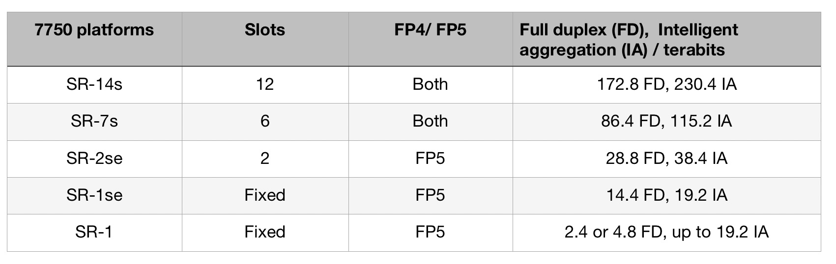
The platforms using the FP5 are the existing 7750 SR-14s and 7750-SR7s routers that were announced with the launch of the FP4.
These chassis were designed to accommodate Nokia’s current and next-generation router cards. “This allows operators to retain the same chassis and support a mix of FP4 and FP5 cards, growing into them gradually,” says Adams.
Nokia has announced three other platforms: two mid-range platforms, the 7750 SR2-se and the 7750 SR1-se, and the 7750 SR-1 that will be available in six variants. “They [the SR-1 boxes] are going to be available in a range of configurations and different port speeds,” says Adams.
Platforms using the FP5 chipset will ship in the first half of 2022, starting with the SR-1.
Nokia also announced an FP5 expandable media adaptor (XMA) line card for the non-fixed platforms (the 7750 SR-14s/ SR-7s and SR-2se). The card supports 36 pluggable slots and with 400 Gigabit Ethernet (GbE) has a capacity of 14.4Tbps full-duplex or 19.2Tbps in intelligent aggregation mode.
The card will also support 400ZR and ZR+ coherent modules and is ready for 800GbE pluggables that will double the card’s capacity ratings.
Nokia says the FP5 improves the throughput of the XMA card by a factor of three: Nokia’s 4.8Tbps XMA (12Tbps IA) uses four FP4 chipsets while the latest 14.4Tbps (19.2Tbps IA) XMA uses six FP5 chipsets.
Custom silicon versus disaggregated designs
Nokia says the benefits of having its own chipset justify the intellectual effort and development expense, even when advanced merchant silicon is available and certain CSPs are embracing open disaggregated routers.
“We feel there is a need in the industry for platforms based on this kind of technology,” says Adams.
What is important is the total cost of ownership and that Nokia’s systems are deployed in critical networks where resiliency, reliability, the feature set and network security are all critical, says Adams.
Nokia also points to the progress it has made since the launch of the FP4. “We have secured 350 projects, two-thirds of which were new footprints or competitive displacements,” says Adams. Nokia’s IP revenues in 2020 were $3.2 billion.
That said, Nokia also partners with merchant silicon vendors: the 7250 IXR interconnect router uses merchant silicon, for example.
“If I look at disaggregation, absolutely, it is an interesting area,” says Adams. “But I think it is very early days.”
Neil McRae, managing director and chief architect at BT, says that while some operators are looking at disaggregated software and hardware, BT doesn’t believe this is necessarily the best solution in terms of performance, reliability or cost.

“Increasingly, the ratio of capital investment in core networking is moving towards optical transceivers than router silicon,” says McRae. “But to get the most out of the network and the router, using custom silicon for the most demanding cases still delivers the best outcomes.
“In our live network but also in our testing, the integrated solution is more reliable, easier to operate and a significant improvement from a total cost of ownership point of view,” says McRae.
BT says it will be able to scale interfaces on the 7750 from 1-400Gbs using the FP5 and Nokia’s SR-OS routing networking software.
BT also highlights the importance of reliability under demand, pointing out how the CSP’s traffic has doubled during the pandemic without impacting its customers.
“Nokia’s understanding of how the underlying silicon is going to react in different situations gives them a significant advantage in building the software on top that performs in challenging situations,” says McRae.
Chip Strategy
Nokia says that were it to sell its FP5 silicon as a standalone product, it would enter a very different design environment.
“You are designing to the requirements of multiple customers versus designing for your systems,” says Adams.
Nokia’s belief is that there is strong demand for platforms designed to purpose.
“We are staying true to that strategy,” says Adams.

Nokia adds 400G coherent modules across its platforms

Nokia is now shipping its 400-gigabit coherent multi-haul CFP2-DCO. The module exceeds the optical performance of 400ZR and ZR+ coherent pluggables.
Nokia’s CFP2-DCO product follows its acquisition of silicon photonics specialist, Elenion Technologies, in 2020.
Nokia has combined Elenion’s coherent optical modulator and receiver with its low-power 64-gigabaud (GBd) PSE-Vc coherent digital signal processor (DSP).
Nokia is also adding coherent pluggables across its platform portfolio.
“Not just optical transport and transponder platforms but also our IP routing portfolio as well,” says Serge Melle, director of product marketing, IP-optical networking at Nokia.
“This [amplifier and filter] allows for much better optical performance,”
“This [amplifier and filter] allows for much better optical performance,”
Melle is an optical networking industry veteran. He joined Nokia two years ago after a 15-year career at Infinera. Melle started at Pirelli in 1995 when it was developing a 4×2.5-gigabit wavelength-division multiplexing (WDM) system. In between Pirelli and Infinera, Melle was at Nortel Networks during the optical boom.
400ZR, ZR+ and the multi-haul CFP2-DCO
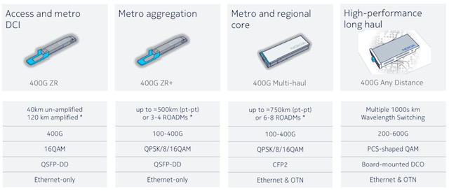
The CFP2-DCO’s optical performance exceeds that of the QSFP-DD and OSFP form factors implementing 400ZR and ZR+ but is inferior to line-card coherent transponders used for the most demanding optical transport applications.
The 400ZR coherent OIF standard transmits a 400-gigabit wavelength up to 120km linking equipment across data centres. Being a standard, 400ZR modules are interoperable.
The ZR+ adds additional transmission speeds – 100, 200 and 300-gigabits – and has a greater reach than ZR. ZR+ is not a standard but there is the OpenZR+ multi-source agreement (MSA).
Implementing 400ZR and ZR+ coherent modules in a QSFP-DD or OSFP module means they can be inserted in client-side optics’ ports on switches and routers.
The OIF did not specify a form factor as part of the 400ZR standard, says Melle, with the industry choosing the QSFP-DD and OSFP. But with the modules’ limited power dissipation, certain modes of the coherent DSP are turned off, curtailing the feature set and the reach compared to a CFP2-DCO module.
The modules also have physical size restrictions.
“You don’t have enough thermal budget to put an optical amplifier inside the QSFP-DD package,” says Melle. “So you are left with whatever power the DWDM laser outputs through the modulator.” This is -7dBm to -10dBm for 400ZR and ZR+ optics, he says.
The CFP2-DCO is larger such that the DSP modes of encryption, OTN client encapsulation, LLDP snooping (used to gather data about attached equipment), and remote network monitoring (RMON) can be enabled.
The CFP2-DCO can also house an optical amplifier and tunable filter. The filter reduces the out-of-band optical signal-to-noise ratio (OSNR) thereby increasing the module’s sensitivity. “This [amplifier and filter] allows for much better optical performance,” says Melle. A 400-gigabit multi-haul module has a 0dBm optical output power, typically.
The different transceiver types are shown in the table.
Nokia’s paper at the recent OFC virtual conference and exhibition detailed how its 400-gigabit multi-haul CFP2-DCO achieved a reach of 1,200km.
The paper details the transmission of 52, 400-gigabit signals, each occupying a 75GHz channel, for a total capacity of 20.8 terabits-per-second (Tbps).
Melle stresses that the demonstration was more a lab set-up than a live network where a signal goes through multiple reconfigurable optical add-drop multiplexers (ROADMs) and where amplifier stages may not be equally spaced.
That said, the CFP2-DCO’s reach in such networks is 750km, says Nokia.
IP-optical integration
Having coherent pluggables enables 400 Gigabit Ethernet (400GbE) payloads to be sent between routers over a wide area network, says Nokia.
“Given this convergence in form factor, with the QSFP-DD and ZR/ ZR+, you can now do IP-optical integration, putting coherent optics on the router without sacrificing port density or having locked-in ports,” says Melle.
Nokia is upgrading its IP and optical portfolio with coherent pluggables.
“In the routers, ZR/ ZR+, and in transponders not only the high-performance coherent optics – the [Nokia] PSE-Vs [DSP] – but also the CFP2-DCO multi-haul,” says Melle. “The 400-gigabit multi-haul is also going to be supported in our routers.”
Accordingly, Nokia has developed two sets of input-output (I/O) router cards: one supporting QSFP-DDs suited for metro-access applications, and the second using CFP2-DCO ports for metro and regional networks.
The choice of cards adds flexibility for network operators; they no longer need to have fixed CFP2-DCO slots on their router faceplates, whether they are used or not. But being physically larger, there are fewer CFP2-DCO ports than QSFP-DD ports on the I/O cards.
While the QSFP-DD MSA initially defined the module with a maximum power dissipation of 14.5W, a coherent QSFP-DD module consumes 18-20W. Dissipating the heat generated by the modules is a challenge.
Nokia’s airflow cooling is simplified by placing a module on both sides of the line card rather than stacking two CFP2-DCOs, one on top of the other.
Nokia is adding its CFP2-DCO to its 1830 optical transport portfolio. These include its PSI-M compact modular systems, the PSS transponder systems and also its PSS-x OTN switching systems.
The 400ZR/ZR+ module will be introduced with all its routing platforms this summer – the 7250 IXR, 7750 SR, 7750 SR-s, and the 7950 XRS, whereas the CFP2-DCO will be added to its 7750 and 7950 series later this year.
Nokia will source the 400ZR/ZR+ from third parties as well as from its optical networks division.
Its routers use QSFP-DD form-factor for all 400GbE ports and this is consistent for most router vendors in the industry. “Thus, our use and supply of 400ZR/ZR+ pluggable DCOs will focus on the QSFP-DD form-factor,” says Melle. However, the company says it can offer the OSFP form-factor depending on demand.
Network planning study
Nokia published a paper at OFC on the ideal coherent solution for different applications.
For metro aggregation rings with 4-5 nodes and several ROADM pass-throughs, using ZR+ modules is sufficient. Moreover, using the ZR+ avoids any loss in router port density.
For metro-regional core applications, the ZR+’s optical performance is mostly insufficient. Here, the full 400-gigabit rate can not be used but rather 300 gigabit-per-second (Gbps) or even 200Gbps to meet the reach requirements.
Using a 400-gigabit multi-haul pluggable on a router might not match the density of the QSFP-DD but it enables a full 400-gigabit line rate.
For long-haul, the CFP2-DCO’s performance is “reasonable”, says Nokia, and this is where high-performance transponders are used.
What the OFC paper argues is that there is no one-size-fits-all solution, says Melle.
800-Gigabit coherent pluggables
Traditionally, the IEEE has defined short-reach client-side optics while the OIF defines coherent standards.
“If we want this IP-optical convergence continuing in the next generation of optics, those two worlds are going to have to collaborate more closely,” says Melle.
That’s because when a form-factor MSA will be defined, it will need to accommodate the short-reach requirements and the coherent optics. If this doesn’t happen, says Melle, there is a risk of a new split occuring around the IP and optical worlds.
The next generation of coherent pluggables will also be challenging.
All the vendors got together in 2019 and said that 400ZR was just around the corner yet the modules are only appearing now, says Melle.
The next jump in pluggable coherent optics will use a symbol rate of 90-130GBd.
“That is very much the cutting-edge so it brings back the optics as a critical enabling technology, and not just optics but the packaging,” concludes Melle.
Nokia shares its vision for cost-reduced coherent optics
Nokia explains why coherent optics will be key for high-speed short-reach links and shares some of its R&D activities. The latest in a series of articles addressing what next for coherent.
Part 3: Reducing cost, size and power
Coherent optics will play a key role in the network evolution of the telecom and webscale players.
The modules will be used for ever-shorter links to enable future cloud services delivered over 5G and fixed-access networks.
The first uses will be to link data centres and support traffic growth at the network edge.
This will be followed with coherent optics being used within the data centre, once traffic growth requires solutions that 4-level pulse-amplitude modulation (PAM4) direct-detect optics can no longer address.
“If you look at PAM4 up to 100 gigabit for long reach and extended reach optics – distances below 80km – it does not scale to higher data rates,” says Marc Bohn, part of product management for Nokia’s optical subsystem group. ”It only scales if you use 100-gigabit in parallel.”
However, to enable short-reach coherent optics, its cost, size and power consumption will need to be reduced significantly. Semiconductor packaging techniques will need to be embraced as will a new generation of coherent digital signal processors (DSPs).
Capacity growth
The adoption of network-edge and on-premise cloud technologies are fueling capacity growth, says Tod Sizer, smart optical fabric & devices research lab leader at Nokia Bell Labs.
Nokia says capacity growth is at 50 per cent per annum and is even faster within the data centre; for every gigabyte entering a data centre, ten gigabytes are transported within the data centre.
“All of this is driving huge amounts of growth in optical capacity at shorter distances,” says Sizer. “To meet that [demand], we need to have coherent solutions to take over where PAM-4 stops.”
Sizer oversees 130 engineers whose research interests include silicon photonics, coherent components and coherent algorithms.
Applications
As well as data centre interconnect, coherent optics will be used for 5G, access and cable networks; markets also highlighted by Infinera and Acacia Communications.

Nokia says the first driver is data centre interconnect.
The large-scale data centre operators triggered the market for 80-120km coherent pluggables with the 400ZR specification for data centre interconnect.
“Right now, with the different architectures in data centres, these guys are saying 80-120km may be an overshoot, maybe we need something for shorter distances to be more efficient,” says Bohn. “Certainly, coherent can tackle that and that is what we are preparing for because there is no alternative, only coherent can cover that space.”
5G is also driving the need for greater bandwidth.
“Traditionally a whole load of processing has been done at the remote ratio head but increasingly, for cost and performance reasons, people are looking at pulling the processing back into the data centre,” says Sizer.
Another traffic driver is how each cellular antenna has three sectors and can use multiple frequency bands.
“Some research we are looking at requires 400 gigabits and above,” says Sizer. “If you want to do a full [mobile] front haul for a massive MIMO (multiple input, multiple output) array, for example.”
Challenges
Several challenges need to be overcome before coherent modules are used widely for shorter-reach links.
To reduce coherent module cost, the optics and DSP need to be co-packaged, borrowing techniques developed by the chip industry.
“Optical and electrical should be brought close together,” says Bohn. “[They should be] co-designed and co-packaged, and the ideal candidate for that is to combine silicon photonics and the DSP.”
The aim is to turn complex designs into a system-on-chip. “Both [the DSP and silicon photonics] are CMOS and you can apply 2D and 3D [die] stacking multi-chip module techniques,” says Bohn, who contrasts it with the custom and manual manufacturing techniques used today.
The coherent DSP also needs to be much simpler than the high-end DSPs used for long-distance optical transport.
For example, the dispersion compensation, which accounts for a significant portion of the chip’s circuitry, is less demanding for shorter links. The forward-error-correction scheme used can also be relaxed as can the bit precision of the analogue-to-digital and digital-to-analogue converters.
Nokia can co-design the silicon photonics and the DSP following its acquisition of Elenion. Nokia is also exploiting Elenion’s packaging know-how and the partnerships it has developed.
Inside the data centre
Nokia highlights two reasons why coherent will eventually be used within the data centre.
The first is the growth in capacity needed inside the data centre. “For the same reason we believe coherent will be the right solution for data centre interconnect and access, the same argument can be made within the data centre,” says Sizer.
A campus data centre is distributed across several buildings and linking them is driving a need for 400-gigabit lanes or more.
This requires a ZR-like solution but for 2km or so rather than 80km.
“It is one of the solutions certainly but that will be driven an awful lot by whether we can make cost-effective solutions to meet the cost targets of the data centre,” says Sizer. That said, there are other ways this can be addressed such as adding fibre.
“Having parallel systems is another area of ongoing research,” says Sizer. “We may need to have unique solutions if traffic grows faster inside the data centre than outside such as spatial-division multiplexing as well as coherent.”
The use of coherent interfaces for networking inside the data centre will take longer.
Bohn points out that 51.2-terabit and 102.4-terabit switches will continue to be served using direct-detect optics but after that, it is unclear because direct-detect optics tops out at 100-gigabits or perhaps 200-gigabits per lane.
“With coherent, it is much easier to get to higher data rates especially over shorter distances,” says Bohn.
Another development benefitting the use of coherent is the next Ethernet standard after 400 Gigabit Ethernet (GbE).
“My research team is looking at that and, in particular, 1.6 Terabit Ethernet (TbE) which is fairly out in the future,” says Sizer. “It will demand a coherent solution, as I expect 800GbE will as well.”
Work to define the next Ethernet standard is starting now and will only be completed in 2025 at the earliest.

Coherent gets a boost with probabilistic shaping
Nokia has detailed its next-generation PSE-3 digital signal processor (DSP) family for coherent optical transmission.
The PSE-3s is the industry’s first announced coherent DSP that supports probabilistic constellation shaping, claims Nokia.
Probabilistic shaping is the latest in a series of techniques adopted to improve coherent optical transmission performance. These techniques include higher-order modulation, soft-decision forward error correction (SD-FEC), multi-dimensional coding, Nyquist filtering and higher baud rates.
 Kyle Hollasch
“There is an element here that the last big gains have now been had,” says Kyle Hollasch, director of product marketing for optical networks at Nokia.
Probabilistic shaping is a signal-processing technique that squeezes the last bit of capacity out of a fibre’s spectrum, approaching what is known as the non-linear Shannon Limit.
“We are not saying we absolutely hit the Shannon Limit but we are extremely close: tenths of a decibel whereas most modern systems are a couple of decibels away from the theoretical maximum,” says Hollasch.
Satisfying requirements
Optical transport equipment vendors are continually challenged to meet the requirements of the telcos and the webscale players.
One issue is meeting the continual growth in IP traffic: telcos are experiencing 25 percent yearly traffic growth whereas for the webscale players it is 60 percent. Vendors must also ensure that their equipment keeps reducing the cost of transport when measured as the cost-per-bit.
Operators also want to automate their networks. Technologies such as flexible-grid, reconfigurable optical add/drop multiplexers (ROADMs), higher-order modulation and higher baud rates all add flexibility to the optical layer but at the expense of complexity.
There is an element here that the last big gains have now been had
“It is easy to say software-defined networking will hide all that complexity,” says Hollasch. “But hardware has an important role: to keep delivering capacity gains but also make the network simpler.”
Satisfying these demands is what Nokia set out to achieve when designing the PSE-3s.
Capacity and cost
Like the current PSE-2 coherent DSPs that Nokia launched in 2016, two chips make up the PSE-3 family: the super coherent PSE-3s and the low-power compact PSE-3c.
The PSE-3s is a 1.2-terabit chip that can drive two sets of optics, each capable of transmitting 100 to 600 gigabit wavelengths. This compares to the 500-gigabit PSE-2s that can drive two wavelengths, each up to 250Gbps.
The low-power PSE-3c also can transmit more traffic, 100 and 200-gigabit wavelengths, twice the capacity of the 100-gigabit PSE-2c.
Nokia has used a software model of two operators’ networks, one an North America and another in Germany, to assess the PSE-3s.
The PSE-3s’ probabilistic shaping delivers 70% more capacity while using a third fewer line cards when compared with existing commercial systems based on 100Gbps for long haul and 200Gbps for the metro. When the PSE-3s is compared with existing Nokia PSE-2s-based platforms on the same networks, a 25 percent capacity gain is achieved using a quarter fewer line cards.
Hollasch says that the capacity gain is 1.7x and not greater because 100-gigabit coherent technology used for long haul is already spectrally efficient. “But it is less so for shorter distances and you do get more capacity gains in the metro,” says Hollasch.
Probabilistic shaping
The 16nm CMOS PSE-3s supports a symbol rate of up to 67Gbaud. This compares to the 28nm CMOS PSE-2s that uses two symbol rates: 33Gbaud and 45Gbaud.
The PSE-3s’ higher baud rate results in a dense wavelength-division multiplexing (DWDM) channel width of 75GHz. Traditional fixed-grid channels are 50GHz wide. With 75GHz-wide channels, 64 lightpaths can fit within the C-band.
The PSE-3s uses one modulation format only: probabilistic shaping 64-ary quadrature amplitude modulation (PS-64QAM). This compares with the PSE-2s that supports six modulations ranging from binary phase-shift keying (BPSK) for the longest spans to 64-QAM for a 400-gigabit wavelength.
Using probabilistic shaping, one modulation format supports data rates from 200 to 600Gbps. For 100Gbps, the PSE-3s uses a lower baud rate in order to fit existing 50GHz-wide channels.
In current optical networks, all the constellation points of the various modulation formats are used with equal probability. BPSK has two constellation points while 64-QAM has 64. Probabilistic shaping does not give equal weighting to all the constellation points. Instead, it favours those with lower energy, represented by those points closer to the origin in a constellation graph. The only time all the constellation points are used is at the maximum data rate - 600Gbps for the PSE-3s.
Using the inner, lower energy constellation points more frequently than the outer points reduces the overall average energy and this improves the signal-to-noise ratio. That is because the symbol error rate at the receiver is dominated by the distance between neighbouring points on the constellation. Reducing the average energy still keeps the distance between the points the same, but since a constant signal power level is used for DWDM transmission, applying gain increases the distance between the constellation points.
“We separate these points further in space - the Euclidean distance between them,” says Hollasch. “That is where the shaping gain comes from.”
Changing the probabilistic shaping in response to feedback from the chip, from the network, we think that is a powerful innovation
Using probabilistic shaping delivers a maximum 1.53dB of improvement in a linear transmission channel. In practice, Nokia says it achieves 1dB. “One dB does not sound a lot but I call it the ultimate dB, the last dB in addition to all the other techniques,” he says.
By using few and fewer of the constellation points, or favouring those points closer to the origin, reduces the data that can be transported. This is how the data rate is reduced from the maximum 600Gbps to 200Gbps.
To implement probabilistic shaping, Nokia has developed an IP block for the chip called the distribution matcher. The matcher maps the input data stream as rates as high as 1.2 terabits-per-second onto the constellation points in a non-uniform way.
Theoretically, probabilistic shaping allows any chosen data rate to be used. But what dictates the actual data rate gradations is the granularity of the client signals. The Optical Internetworking Forum’s Flex Ethernet (FlexE) standard defines 25-gigabit increments and that will be the size of the line-side data rate increments.
Embracing a single modulation format and a 75GHz channel results in network operation benefits, says Hollasch: “It stops you having to worry and manage a complicated spectrum across a broad network.” And it also offers the prospect of network optimisation. “Changing the probabilistic shaping in response to feedback from the chip, from the network, we think that is a powerful innovation,” says Hollasch.
 The reach performance of the PSE-3s using 62Gbaud and PS-64QAM. The reach performance of the PSE-2s is shown (where relevant) for comparison purposes.
Product plans
The first Nokia product to use the PSE-3 chips is the 1830 Photonic Service Interconnect-Modular, a 1 rack-unit compact modular platform favoured by the webscale players.
Nokia has designed two module-types or ‘sleds’ for the 1830 PSI-M pizza box. The first is a 400-gigabit sled that uses two sets of optics and two PSE-3c chips along with four 100-gigabit client-side interfaces. Four such 400-gigabit sleds fit within the platform to deliver a total of 1.6 terabits of line-side capacity.
In contrast, two double-width sleds fit within the platform using the PSE-3s. Each sled has one PSE-3 chip and two sets of optics, each capable of up to a 600-gigabit wavelength, and a dozen 100-gigabit interfaces. Here the line-side capacity is 2.4 terabits.
Nokia says the 400-gigabit sleds will be available in the first half of this year whereas the 1.2 terabit sleds will start shipping at the year-end or early 2019. The first samples of the PSE-3s are expected in the second half of 2018. Nokia will then migrate the PSE-3s to the rest of its optical transport platform portfolio.
So has coherent largely run its course?
“In terms of a major innovation in signal processing, probabilistic shaping is completing the coherent picture,” says Hollasch. There will be future coherent DSP chips based on more advanced process nodes than 16nm with symbol rates approaching 100GBaud. Higher data rates per wavelength will result but at the expense of a wider channel width. But once probabilistic shaping is deployed, further spectral efficiencies will be limited.