
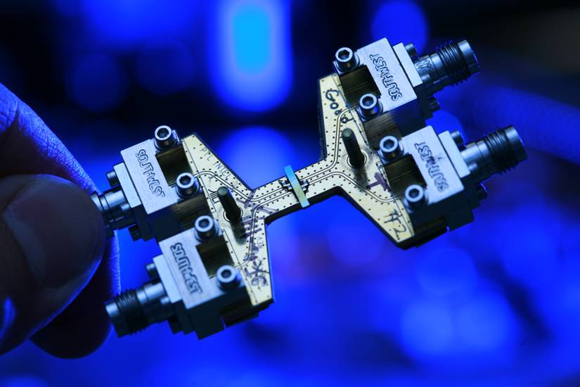
MACOM acquires Mindspeed to boost 100 Gig offerings
 Ray MoroneyThe Mindspeed acquisition increases the serviceable addressible market for MACOM, both geographical - the company will strengthen its presence in Asia Pacific - and by gaining new equipment vendor accounts. It also broadens MACOM's 100 Gigabit physical device portfolio.
"We are targeting the 100 Gig buildout and the growth coming from that," says Ray Moroney, product line manager, opto-device business unit at MACOM.
Mindpeed also makes a broad portfolio of crosspoint switches used in datacom equipment, and several families of communications processors.
With the acquisition of Mindspeed we have the full electronics bill-of-materials for CFP2 and CFP4 [module] client-side applications
MACOM entered opto-electronics with the acquisition of Optimai in 2011 that had long-haul and client-side modulator drivers and trans-impedance amplifiers (TIAs). Now with Mindspeed's products, MACOM can capture client-side designs with clock data recovery chips and quad-channel TIAs for 100 Gig modules. "With the acquisition of Mindspeed we have the full electronics bill-of-materials for CFP2 and CFP4 [module] client-side applications," says Moroney.
MACOM also gains silicon germanium technology alongside its indium phosphide and gallium arsenide technologies. Silicon germanium has a lower cost structure once a design is being made in volume production, says Moroney, but the R&D and mask costs are generally higher. Silicon germanium also allows significant integration. "It is BiCMOS in nature," says Moroney. "You can integrate full CMOS functionality into a design too." For example digital control can be added alongside analogue functions. Moroney says the company will use silicon germanium for high-performance analogue designs like TIAs as well as high-frequency millimeter wave and microwave applications.
The company is considering its options regarding the future of the communications processors arm of Mindspeed's business. "MACOM is very much an analogue/ RF company," says Moroney. "It [communications processors] is certainly not seen as a core area of investment for MACOM."
Terabit interconnect to take hold in the data centre
Intel and Corning have further detailed their 1.6 Terabit interface technology for the data centre.
The collaboration combines Intel's silicon photonics technology operating at 25 Gigabit-per-fibre with Corning's ClearCurve LX multimode fibre and latest MXC connector.
 Silicon photonics wafer and the ClearCurve fibres. Source: Intel
The fibre has a 300m reach, triple the reach of existing multi-mode fibre at such speeds, and uses a 1310nm wavelength. Used with the MXC connector that supports 64 fibres, the overall capacity will be 1.6 Terabits-per-second (Tbps).
"Each channel has a send and a receive fibre which are full duplex," says Victor Krutul, director business development and marketing for silicon photonics at Intel. "You can send 0.8Tbps on one direction and 0.8Tbps in the other direction at the same time."
The link supports connections within a rack and between racks; for example, connecting a data centre's top-of-rack Ethernet switch with an end-of-row one.
James Kisner, an analyst at global investment banking firm, Jefferies, views Intel’s efforts as providing important validation for the fledgling silicon photonics market.
However, in a research note, he points out that it is unclear whether large data centre equipment buyers will be eager to adopt the multi-mode fibre solution as it is more expensive than single mode. Equally, large data centres have increasingly longer span requirements - 500m to 2km - further promoting the long term use of single mode fibre.
Rack Scale Architecture
The latest details of the silicon photonics/ ClearCurve cabling were given as part of an Intel update on several data centre technologies including its Atom C2000 processor family for microservers, the FM5224 72-port Ethernet switch chip, and Intel's Rack Scale Architecture (RSA) that uses the new cabling and connector.
Intel is a member of Facebook's Open Compute Project based on a disaggregated system design that separates storage, computing and networking. "When I upgrade the microprocessors on the motherboard, I don't have to throw away the NICs [network interface controllers] and disc drives," says Krutul. The disaggregation can be within a rack or between rows of equipment. Intel's RSA is a disaggregated design example.
The chip company discussed an RSA design for Facebook. The rack has three 100Gbps silicon photonics modules per tray. Each module has four transmit and four receive fibres, or 24 fibres per tray and per cable. “Different versions of RSA will have more or less modules depending on requirements," says Krutul. Intel has also demonstrated a 32-fibre MXC prototype connector.
Corning says the ClearCurve fibre delivers several benefits. The fibre has a smaller bend radius of 7.5mm, enabling fibre routing on a line card. The 50 micron multimode fibre face is also expanded to 180 microns using a beam expander lens. The lenses make connector alignment easier and less sensitive to dust. Corning says the MXC connector comprises seven parts, fewer than other optical connectors.
Fibre and connector standardisation are key to ensure broad use, says Daryl Inniss, vice president and practice leader, components at Ovum.
"Intel is the only 1310nm multimode transmitter and receiver supplier, and expanding this optical link into other applications like enterprise data centres may require a broader supply base," says Inniss in a comment piece. But the fact that Corning is participating in the development signals a big market in the making, he says.
Intel has not said when the silicon photonics transceiver and fibre/ connector will be generally available. "We are not discussing schedules or pricing at this time," says Krutul.
Silicon photonics: Intel's first lab venture
The chip company has been developing silicon photonics technology for a decade.
"As our microprocessors get faster, you need bigger and faster pipes in and around the servers," says Krutul. "That is a our whole goal - feeding our microprocessors."
Intel is setting up what it calls 'lab ventures', with silicon photonics chosen to be the first.
"You have a research organisation that does not do productisation, and business units that just do products," says Krutul. "You need something in between so that technology can move from pure research to product; a lab venture is an organisational structure to allow that movement to happen."
The lab ventures will be discussed more in the coming year.
Mellanox to acquire silicon photonics player Kotura
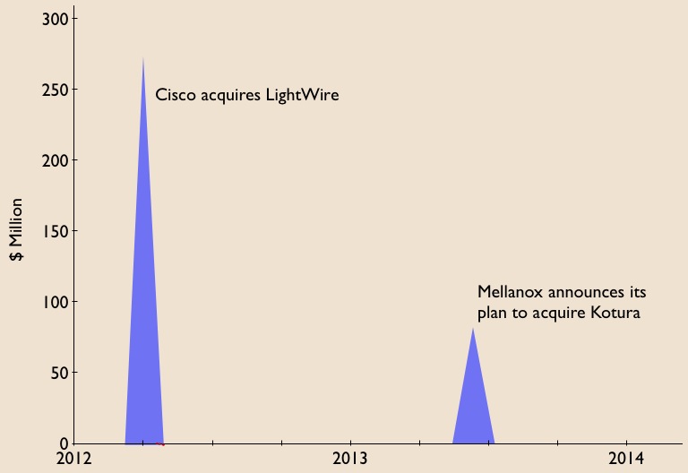 Source: Gazettabyte
Mellanox Technologies has announced its intention to acquire silicon photonics player, Kotura, for $82 million.
The acquisition will enable Mellanox to deliver 100 Gigabit Infiniband and Ethernet interconnect in the coming two years. lt will also provide Kotura with the resources needed to bring its 100 Gigabit QSFP to market. Mellanox will also gain Kotura's optical engine for use in active optical cables and new mid-plane platform designs, as well as future higher speed interfaces.
The news is also significant for the optical component industry. Kotura is one of the three established merchant silicon photonics players - the others being LightWire and Luxtera - that have spent years developing their technologies.
LightWire was acquired by Cisco Systems in March 2012 for US $271 million and now Mellanox plans to acquire Kotura. The two equipment vendors recognise the value of the technology, bringing it in-house to reduce system interconnect costs and as a long term differentiator for their equipment and ASIC designs. Mellanox, as a silicon photonics player, will compete with Intel, with its own silicon photonics technology, and Cisco Systems.
Kotura has been using its technology to sell telecom products such as variable optical attenuators and multiplexers. The start-up recently announced its 100 Gig QSFP that uses wavelength division multiplexing (WDM) transmitter and receiver chips. The product is to become available in 2014.
In an interview last year, Kotura's CTO, Mehdi Asghari, discussed a roadmap showing how its 100 Gigabit silicon photonics technology could scale to 400 Gigabit and eventually 1.6 Terabit.
"Our devices are capable of running at 40 or 50 Gigabit-per-second (Gbps), depending on the electronics. The electronics is going to limit the speed of our devices. We can very easily see going from four channels at 25Gbps to 16 channels at 25Gbps to provide a 400 Gigabit solution," Asghari told Gazettabyte.
Kotura also discussed how the line rate could be increased to 50Gbps either using a non-return-to-zero (NRZ) line rate or using a multi-level modulation such as pulse amplitude modulation (PAM).
"To get to 1.6 Terabit transceivers, we envisage something running at 40Gbps times 40 channels or 50Gbps times 32 channels. We already have done a single receiver chip demonstrator that has 40 channels, each at 40Gbps," said Asghari.
"These things in silicon are not a big deal. The III-V guys really struggle with yield and cost. But you can envisage scaling to that level of complexity in a silicon platform."
Silicon photonics will not replace existing VCSEL or indium phosphide-based transceiver designs. But there is no doubting silicon photonics is emerging as a key optical technology and the segment is heating up.
If the early start-ups are being acquired, there have been more recent silicon photonics players entering the marketplace such as Aurrion, Skorpios Technologies and Teraxion. There are also internal developments among equipment players such as Alcatel-Lucent, HP Labs and IBM. Indeed Kotura has worked closely with Oracle (Sun Microsystems)
Further acquisitions of silicon photonic players should be expected as companies start designing next generation, denser systems and adopt 100 Gigabit and faster interfaces.
Equally, established optical component and module companies will likely enter quietly (and not so quietly) the marketplace adding silicon photonics to their technology toolkits when the timing is right.
Trends to watch
Two industry trends are underway regarding silicon photonics.
The first is system vendors wanting to own the technology to reduce their costs while recognising a need to control and understand the technology as they tackle more complex equipment designs.
The other, what at first glance is a contrarian trend, is the democratisation of silicon photonics.
The technology is slowly passing from the select few to become more generally available for industry use. For this to happen, the relevant design tools need to mature as do third-party fabrication plants that will manufacture the silicon photonics designs.
Appendix:
On June 4th, 2013, Mellanox announced a definitive agreement to acquire chip company IPtronics for $47.5 million as it builds out its in-house technologies for optical interconnect. Click here
Futher reading:
Avago to acquire CyOptics, click here
Oclaro points its laser diodes at new markets

“To succeed in any market ... you need to be the best at something, to have that sustainable differentiator”
Yves LeMaitre, Oclaro
Now LeMaitre is executive vice president at Oclaro, managing the company’s advanced photonics solutions (APS) arm. The APS division is tasked with developing non-telecom opportunities based on Oclaro’s high-power laser diode portfolio, and accounts for 10%-15% of the company’s revenues.
“The goal is not to create a separate business,” says LeMaitre. “Our goal is to use the infrastructure and the technologies we have, find those niche markets that need these technologies and grow off them.”
Recently Oclaro opened a design centre in Tucson, Arizona that adds packing expertise to its existing high-power laser diode chip business. The company bolstered its laser diode product line in June 2009 when Oclaro gained the Newport Spectra Physics division in a business swap. “We became the largest merchant vendor for high-power laser diodes,” says LeMaitre.
The products include single laser chips, laser arrays and stacked arrays that deliver hundred of watts of output power. “We had all that fundamental chip technology,” says LeMaitre. “What we have been less good at is packaging those chips - managing the thermals as well as coupling that raw chip output power into fibre.”
The new design centre is focussed on packaging which typically must be tailored for each product.
Laser diodes
There are three laser types that use laser diodes, either directly or as ‘pumps’:
- Solid-state laser, known as diode-pumped solid-state (DPSS) lasers.
- Fibre laser, where the fibre is the medium that amplifies light.
- Direct diode laser - here the semiconductor diode itself generates the light.
All three types use laser diodes that operate in the 800-980nm range. Oclaro has much experience in gallium arsenide pump-diode designs for telecom that operate at 920nm wavelengths and above.
Laser diode designs for non-telecom applications are also gallium arsenide-based but operate at 800nm and above. They are also scaled-up designs, says LeMaitre: “If you can get 1W on a single mode fibre for telecom, you can get 10W on a multi-mode fibre.” Combining the lasers in an array allows 100-200W outputs. And by stacking the arrays while inserting cooling between the layers, several hundreds of watts of output power are possible.
The lasers are typically sold as packaged and cooled designs, rather than as raw chips. The laser beam can be collimated to precisely deliver the light, or the beam may be coupled when fibre is the preferred delivery medium.
“The laser beam is used to heat, to weld, to burn, to mark and to engrave,” says LeMaitre. “That beam may be coming directly from the laser [diode], or from another medium that is pumped by the laser [diode].” Such designs require specialist packaging, says LeMaitre, and this is what Oclaro secured when it acquired the Spectra Physics division.
Applications
Laser diodes are used in four main markets which Oclaro values at US$800 million a year.
One is the mature, industrial market. Here lasers are used for manufacturing tasks such as metal welding and metal cutting, marking and welding of plastics, and scribing semiconductor wafers.
Another is high-quality printing where the lasers are used to mark large printing plates. This, says LeMaitre, is a small specialist market.
Health care is a growing market for lasers which are used for surgery, although the largest segment is now skin and hair treatment.
The final main market is consumer where vertical-cavity surface-emitting lasers (VCSELs) are used. The VCSELs have output powers in the tens or hundreds of milliwatts only and are used in computer mouse interfaces and for cursor navigation in smartphones.
“These are simple applications that use lasers because they provide reliable, high-quality optical control of the device,” says LeMaitre. “We are talking tens of millions of [VCSEL] devices [a year] that we are shipping right now for these types of applications.”
Oclaro is a supplier of VCSELs for Light Peak, Intel’s high-speed optical cable technology to link electronic devices. “There will be adoptions of the initial Light Peak starting the end of this year or early next year, and we are starting to ramp up production for that,” says LeMaitre. “In the meantime, there are many alternative [designs] happening – the market is extremely active – and we are talking to a lot of players.” Oclaro sells the laser chips for such interface designs; it does not sell optical engines or the cables.
Is Oclaro pursuing optical engines for datacom applications, linking large switch and IP router systems? “We are actively looking at that but we haven’t made any public announcements,” he says.
Market status
LeMaitre has been at Oclaro since 2008 when Avanex merged with Bookham (to become Oclaro). Before that, he was CEO at optical component start-up, LightConnect.
How does the industry now compare with that of a decade ago?
“At that time [of the downturn] the feeling was that it was going to be tough for maybe a year or two but that by 2002 or 2003 the market would be back to normal,” says LeMaitre. “Certainly no-one expected the downturn would last five years.” Since then, nearly all of the start-ups have been acquired or have exited; Oclaro itself is the result of the merger of some 15 companies.
“People were talking about the need for consolidation, well, it has happened,” he says. Oclaro’s main market – optical components for metro and long haul transmission – now has some four main players. “The consolidation has allowed these companies, including Oclaro, to reach a level of profitability which has not been possible until the last two years,” says LeMaitre.
Demand for bandwidth has continued even with the recent economic downturn, and this has helped the financial performance of the optical component companies.
“The need for bandwidth has still sustained some reasonable level of investment even in the dark times,” he says. “The market is not as sexy as it was in those [boom] days but it is much more healthy; a sign of the industry maturing.”
Industry maturity also brings corporate stability which LeMaitre says provides a healthy backdrop when developing new business opportunities.
The industrial, healthcare and printing markets require greater customisation than optical components for telecom, he says, whereas the consumer market is the opposite, being characterised by vastly greater unit volumes.
“To succeed in any market – this is true for this market and for the telecom market – you need to be the best at something, to have that sustainable differentiator,” says LeMaitre. For Oclaro, its differentiator is its semiconductor laser chip expertise. “If you don’t have a sustainable differentiator, it just doesn’t work.”
Framing the information age
When writing features for FibreSystems Europe, I repeatedly asked for high-resolution striking images. The magazine's editors always wanted photos that included people, like Maurice Broomfield's photos. Getting hold of such images did happen but not often.
Inspired by the Financial Times’ interview and Maurice Broomfield's beautiful images, some of the better images sent are presented here.
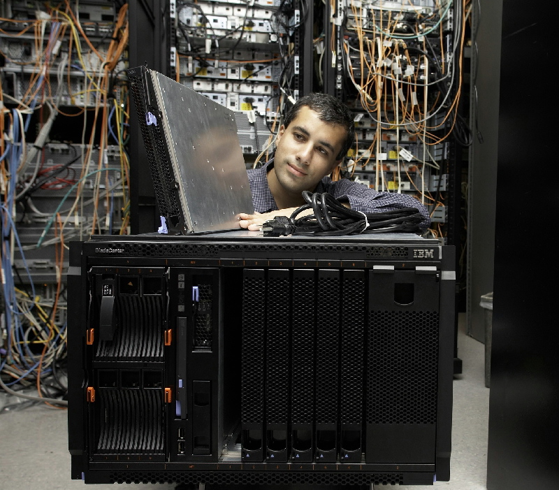 IBM data centre
I’m on the look-out for more. So if you are the media relations for an operator, equipment maker, optical transceiver or component (optical or IC) vendor, can I please request some inspiring photos - ideally with people - and I'll create a photo gallery of the best.
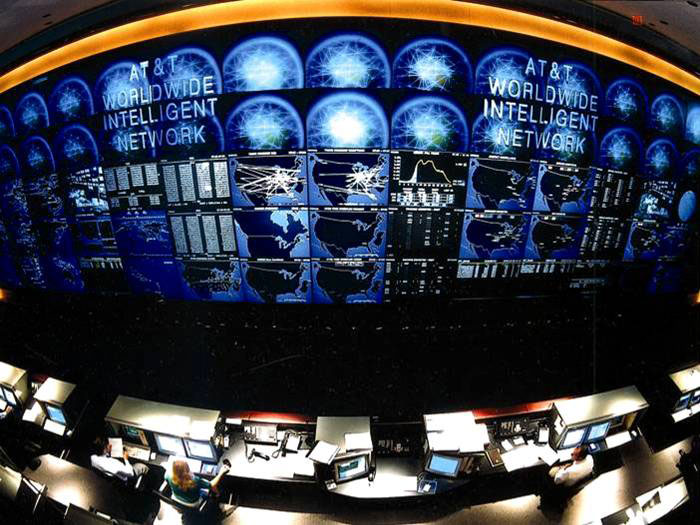 Network Operations Centre (NOC) Source: AT&T
 Source: Cisco Systems
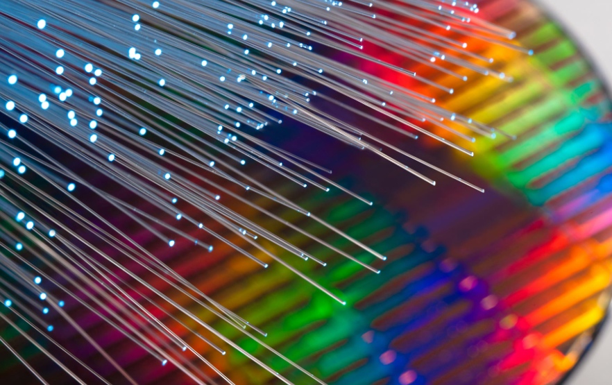
 An Intel silicon photonics device
And here is an image of Tokyo's data centre on Flickr