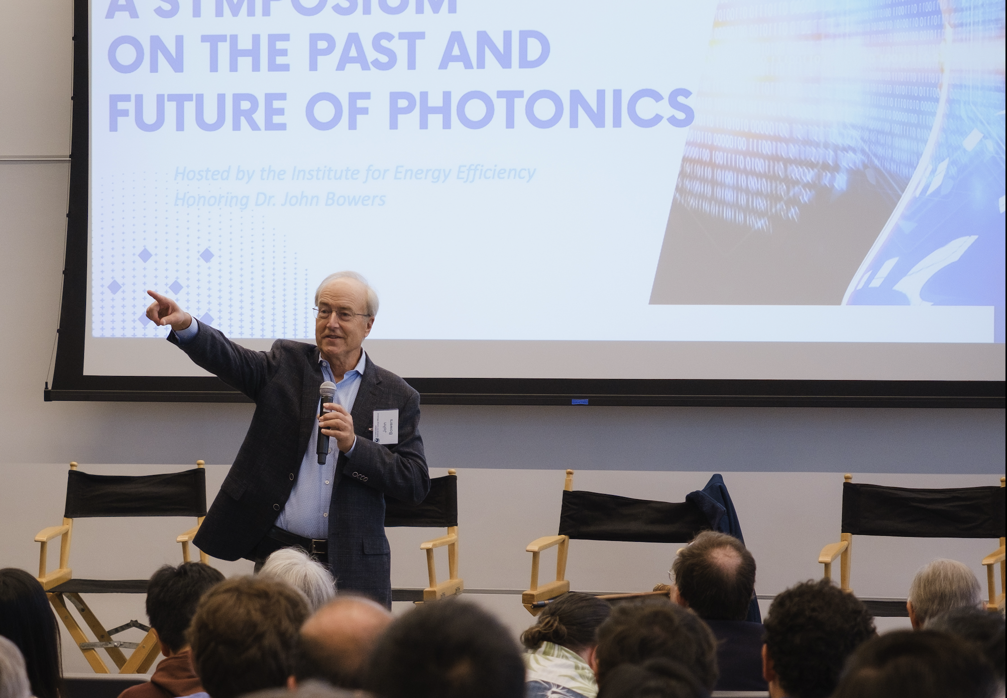
John Bowers: We are still at the dawn of photonics

After 38 years at the University of California, Santa Barbara (UCSB), Professor John Bowers (pictured) is stepping away from teaching and administrative roles to focus on research.
He welcomes the time it will free for biking and golf. He will also be able to linger, not rush, when travelling. On a recent trip to Saudi Arabia, what would have centered around a day-event became a week-long visit.
Bowers’ career includes significant contributions to laser integration and silicon photonics, mentoring some 85 PhD students, and helping found six start-ups, two of which he was the CEO.
Early Influences
Bowers’ interest in science took root while at high school. He built oscilloscopes and power supplies using Heathkits, then popular educational assemblies for electronics enthusiasts. He was also inspired by his physics and chemistry teachers, subjects he majored in at the University of Minnesota.
A challenging experience led him to focus solely on physics: “I took organic chemistry and hated it,” says Bowers. “I went, ‘Okay, let’s stick to inorganic materials.’”
Bowers became drawn to high-energy physics and worked in a group conducting experiments at Fermilab and Argonne National Laboratories. Late-night shifts – 10 PM to 6 AM – offered hands-on learning, but a turning point came when his mentor was denied tenure. “My white knight fell off his horse,” he says.
He switched to applied physics at Stanford, where he explored gallium arsenide and silicon acoustic devices, working under the supervision of the late Gordon Kino, a leading figure in applied physics and electrical engineering.
Bowers then switched to fibre optics, working in a group that was an early leader in single-mode optical fibre. “It was a period when fibre optics was just taking off,” says Bowers. “In 1978, they did the first 50-megabit transmission system, and OFC [the premier optical fibre conference] was just starting.”
Bell Labs and fibre optics
After gaining his doctorate, Bowers joined Bell Labs, where his work focused on the devices—high-speed lasers and photodetectors—used for fibre transmission. He was part of a team that scaled fibre-optic systems from 2 to 16 gigabits per second. However, the 1984 AT&T breakup signalled funding challenges, with Bell Labs losing two-thirds of its financial support.
Seeking a more stable environment, Bowers joined UCSB in 1987. He was attracted by its expertise in semiconductors and lasers, including the presence of the late Herbert Kroemer, who went on to win the 2000 Nobel Prize in Physics. Kroemer developed the double heterostructure laser and played a big part in enticing Bowers to join. Bowers was tasked with continuing the laser work, something he has done for the last 40 years.
“Coming to Santa Barbara was brilliant, in retrospect,” says Bowers, citing its strong collaborative culture and a then newly formed materials department.
Integrated lasers
At UCSB, Bowers worked on integrated circuits using indium phosphide, including tunable lasers and 3D stacking of photonic devices.
At the same time, the field of silicon photonics was starting after Richard Soref wrote a seminal paper proposing silicon as an optical material for photonic integrated circuits (PIC).
“We all knew that silicon was a terrible light emitter because it is an indirect band-gap material,” says Bowers. “So when people started talking about silicon photonics, I kept thinking: ‘Well, that is fine, but you need a light source, and if you don’t have a light source, it’ll never become important.’”
Bowers tackled integrating lasers onto silicon to address the critical need for an on-chip light source. He partnered with Intel’s Mario Paniccia and his team, which had made tremendous progress developing a silicon Raman lasers with higher powers and narrower linewidths.
“It was very exciting, but you still needed a pump laser; a Raman laser is just a wavelength converter from one wavelength to another,” says Bowers. “So I focused on the pump laser end, and the collaboration benefitted us both.”
Intel commercialised the resulting integrated laser design and sold millions of silicon-photonics-based pluggable transceivers.
“Our original vision was verified: the idea that if you have CMOS processing, the yields will be better, the performance will be better, the cost will be lower, and it scales a lot better,” says Bowers. “All that has proven to be true.
Is Bowers surprised that integrated laser designs are not more widespread?
All the big silicon photonics companies, including foundry TSMC, will incorporate lasers into their products, he says, just as Intel has done and Infinera before that.
Infinera, an indium phosphide photonic integrated circuit (PIC) company now acquired by Nokia, claimed that integration would improve the reliability and lower the cost, says Bowers: “Infinera did prove that with indium phosphide and Intel did the same thing for silicon.”
The indium phosphide transceiver has a typical failure rate of 10 FIT (failures per ten billion hours), and if there are 10 laser devices, the FIT rises to 100, he says. By contrast, Intel’s design has a FIT of 0.1, and so with 10, the FIT becomes on the order of 1.
Silicon lasers are more reliable because there’s no III-V material exposed anywhere. Silicon or silicon dioxide facets eliminate the standard degradation mechanisms in III-V materials. This enables non-hermetic packaging, reducing costs and enabling rapid scaling.
According to Bowers, Intel scaled to a million transceivers in one year. Such rapid scaling to high volumes is important for many applications, and that is where silicon photonics has an advantage.
“Different things motivate different people. For me, it’s not about money, it’s more about your impact, particularly on students and research fields. To the extent that I’ve contributed to silicon photonics becoming important and dynamic, that is something I’m proud of.”
-Professor John Bowers
Optical device trends
Bowers notes how the rise of AI has surprised everyone, not just in terms of the number of accelerator chips needed but their input-output (I/O) requirements.
Copper has been the main transmission medium since the beginning of semiconductor chips, but that is now being displaced by optics – silicon photonics in particular – for the communications needs of very high bandwidth chips. He also cites companies like Broadcom and Nvidia shipping co-packaged optics (CPO) for their switching chips and platforms.
“Optics is the only economic way to proceed, you have to work on 3D stacking of chips coupled with modern packaging techniques,” he says, adding that the need for high yield and high reliability has been driving the work on III-V lasers on silicon.
One current research focus for Bowers is quantum dot lasers, which reduce the line width and minimise reflection sensitivity by 40dB. This eliminates the need for costly isolators in datacom transceivers.
Quantum dot devices also show exceptional durability, with lifetimes for epitaxial lasers on silicon a million times longer than quantum well devices on silicon and 10 times less sensitivity to radiation damage, as shown in a recent Sandia National Labs study for space applications.
Another area of interest is modulators for silicon photonics. Bowers says his group is working on sending data at 400 gigabits-per-wavelength using ‘slow light’ modulators. These optical devices modulate the intensity or phase, of light. Slowing down the light improves its interaction in the material, improving efficiency and reducing device size and capacitance. He sees such modulators is an important innovation.
“Those innovations will keep happening; we’re not limited in terms of speed by the modulator,” says Bowers, who also notes the progress in thin-film lithium niobate modulators, which he sees as benefiting silicon photonics, “We have written papers suggesting most of the devices may be III-V,” says Bowers, and the same applies to materials such as thin-film lithium niobate.
“I believe that as photonic systems become more complex, with more lasers and amplifiers, then everyone will be forced to integrate,” says Bowers.
Other applications
Beyond datacom, Bowers sees silicon photonics enabling LIDAR, medical sensors, and optical clocks. His work on low-noise lasers, coupled to silicon nitride waveguides, reduces phase noise by 60dB, enhancing sensor sensitivity. “If you can reduce the frequency noise by 60dB, then that makes it either 60dB more efficient, or you need 60dB less power,” he says.
Applications include frequency-based sensors for gas detection, rotation sensing, and navigation, where resonance frequency shifts detect environmental changes.
Other emerging applications include optical clocks for precise timing in navigation, replacing quartz oscillators. “You can now make very quiet clocks, and at some point we can integrate all the elements,” Bowers says, envisioning chip-scale solutions.
Mentorship and entrepreneurial contributions
Bowers’ impact extends to mentorship, guiding so many PhD students who have gone on to achieve great success.
“It’s very gratifying to see that progression from an incoming student who doesn’t know what an oscilloscope is to someone who’s running a group of 500 people,” he says.
Alan Liu, former student and now CEO of the quantum dot photonics start-up Quintessent, talks about how Bowers calls on his students to ‘change the world’.
Liu says it is not just about pushing the frontiers of science but also about having a tangible impact on society through technology and entrepreneurship.”
Bowers co-founded UCSB’s Technology Management Department and taught entrepreneurship for 30 years. Drawing on mentors like Milton Chang, he focused on common start-up pitfalls: “Most companies fail for the same set of reasons.”
His own CEO start-up experience informed his teaching, highlighting interdisciplinary skills and team dynamics.
Mario Paniccia, CEO of Anello Photonics, who collaborated with Bowers as part of the Intel integrated laser work, highlights Bowers’ entrepreneurial skills.
“John is one of the few professors who are not only brilliant and technically a world expert – in John’s case, in III-V materials – but also business savvy and entrepreneurial,” says Paniccia. “He is not afraid to take risks and can pick and hire the best.”
Photonics’ future roadmap
Bowers compares photonics’ trajectory to electronics in the 1970s, when competing CMOS technologies standardised, shifting designers’ focus from device development to complex circuits. “Just like in the 1970s, there were 10 competing transistor technologies; the same consolidation will happen in photonics,” he says.
Standardised photonic components will be integrated into process design kits (PDKs), redirecting research toward systems like sensors and optical clocks.
“We’re not at the end, we’re at the beginning of photonics,” emphasises Bowers.
Reflections
Looking back, would he have done anything differently?
A prolonged pause follows: “I’ve been very happy with the choices I have made,” says Bowers, grateful for his time at UCSB and his role in advancing silicon photonics.
Meanwhile, Bowers’ appetite for photonics remains unwavering: “The need for photonic communication, getting down to the chip level, is just going to keep exploding,” he says.

A coherent roadmap for co-packaged optics
Is coherent optics how co-packaged will continue to scale? Pilot Photonics certainly thinks so.

Part 1: Co-packaged optics
Frank Smyth, CTO and founder of Pilot Photonics, believes the firm is at an important inflection point.
Known for its comb laser technology, Pilot Photonics has just been awarded a €2.5 million European Innovation Council grant to develop its light-source technology for co-packaged optics.
The Irish start-up is also moving to much larger premises and is on a recruitment drive. “Many of our projects and technologies are maturing,” says Smyth.
Company
Founded in 2011, the start-up spent its early years coupled to Dublin City University. It raised its first notable investment in 2017.
The company began by making lab instrumentation based on its optical comb laser technology which emits multiple sources of light that are frequency- and phased-locked. But a limited market caused the company to pivot, adding photonic integration to its laser know-how.
Now, the start-up has a fast-switching, narrow-linewidth tunable laser, early samples of which are being evaluated by several “tier-one” companies.
Pilot Photonics also has a narrowband indium-phosphide comb laser for optical transport applications. This will be the next product it samples.
More recently, the start-up has been developing a silicon nitride-based comb laser for a European Space Agency project. “The silicon nitride micro-resonator in the comb is a non-linear element that enables a very broad comb for highly parallel communication systems and for scientific applications,” says Smyth. It is this laser type that is earmarked for the data centre and for co-packaged optics applications.
Smyth stresses that while still being a small company, the staff has broad expertise. “We cover the full stack,” he says.
Skills range from epitaxial wafer design, photonic integrated circuit (PIC)s and lasers, radio frequency (RF) and thermal expertise, and digital electronics and control design capabilities.
“We learned early on that it’s all well making a PIC, but if no one can interface to it, you are wasting your time,” says Smyth.
Co-packaged optics
Co-packaged optics refers to adding optics next to an ASIC that has significant input-output (I/O) data requirements. Examples of applications for co-packaged optics include high-capacity Ethernet switch chips and artificial intelligence (AI) accelerators. The goal is to give the chip optical rather than electrical interfaces, providing system-scaling benefits; as electrical signals get faster, their reach shrink.
The industry has been discussing co-packaged optics for over a decade. Switch-chip players and systems vendors have shown prototype designs and even products. And more than half a dozen companies are developing the optical engines that surround, and are packaged with, the chip.
However, the solutions remain proprietary, and while the OIF is working to standardise co-packaged optics, end users have yet to embrace the technology. In part, this is because pluggable optical modules continue to advance in data speeds and power consumption, with developments like linear-drive optics.
The ecosystem supporting co-packaged optics is also developing. Hyperscalers will only deploy co-packaged optics in volume when reliability and a broad manufacturing base are proven.
Yet industry consensus remains that optical I/O is a critical technology and that deployments will ramp up in the next two years. Ethernet switch capacity doubles every two years while AI accelerator chips are progressing rapidly. Moreover, the number of accelerator chips used in AI supercomputers is growing fast, from thousands to tens of thousands.
Pilot Photonics believes its multi-wavelength laser technology, coupled with the intellectual property it is developing, will enable co-packaged optics based on coherent optics to address such scaling issues.
Implementations
Co-packaged optics uses optical chiplets or ‘engines’ that surround the ASIC on a shared substrate. The optical engines typically use an external laser source although certain co-packaged optics solutions such as from Intel and Ranovus can integrate the laser as part of the silicon-photonics based optical engine.
Designers can scale the optical engine’s I/O capacity in several ways. They can increase the number of fibres connected to the optical engine, send more wavelengths down each fibre, and increase the wavelength’s data rate measured in gigabits per second (Gbps).
In co-packaged optics designs, 16 engines typically surround the chip. For a 25.6-terabit Ethernet chip, 16 x 1.6-terabit engines are used, each 1.6-terabit engine sending a 100Gbps DR1 signal per fibre. The total fibres per engine equals 32: 16 for the transmit and 16 for the receive (see table).
| Switch capacity/Tbps | Optical engine/Tbps | Optical engines | Data rate/fibre | No. fibres/ engine* |
| 25.6 | 1.6 | 16 | 100G DR, 500m | 32 |
| 25.6 | 3.2 | 8 | 100G DR, 500m | 64 |
| 51.2 | 6.4 | 8 | 400G FR4, 2km | 32 |
| 102.4 (speculative) | 6.4 | 16 | 400G FR4, 2km | 16 |
| 102.4 (speculation) | 12.8 | 8 | 400G FR4, 2km | 32 |
*Not counting the external laser source fibre.
Broadcom’s co-packaged optical approach uses eight optical engines around its 25.6-terabit Tomahawk 4 switch chip, each with 3.2Tbps capacity. For the Tomahawk 5, 51.2-terabit Bailly co-packaged optics design, Broadcom uses eight, 6.4Tbps optical engines, sending 400-gigabit FR4, or 4-wavelength coarse WDM wavelengths, across each fibre. Using FR4 instead of DR1 halves the number of optical engines while doubling overall capacity.
The co-packaging solutions used in the next-generation 102.4-terabit switch chip are still to be determined. Capacity could be doubled using twice as many fibres, or by using 200-gigabit optical wavelengths based on 112G PAM-4 electrical inputs, twice the speed currently used.
But scaling routes for the generation after that – 204.8-terabit switch chips and beyond – and the co-packaged optics design become unclear due to issues of dispersion and power constraints, says Smyth.
Scaling challenges
Assuming eight engines were used alongside the 200-terabit ASIC , each would need to be 25.6Tbps. The fibre count per engine could be doubled again or more wavelengths per fibre would be needed. One player, Nubis Communications, scales its engines and fibres in a 2D array over the top of the package, an approach suited to fibre-count growth.
Doubling the wavelength count is another option but adopting an 8-wavelength CWDM design with 20nm spacing means the wavelengths would cover 160nm of spectrum. Over a 2km reach, this is challenging due to problems with dispersion. Narrower channel spacings such as those used in the CW-WDM MSA (multi-source agreement) require temperature control to ensure the wavelengths stay put.
Keeping the symbol rate fixed but doubling the data rate is another option. But adopting the more complex PAM-8 modulation brings its own link challenges.
Another key issue is power. Current 51.2-terabit switches require 400mW of laser launch power (4 x 100mW lasers) per fibre and there are 128 transmit fibers per switch.
“Assuming a wall plug efficiency of 20 per cent, that is around 250W of power dissipation just for the lasers,” says Smyth. “Getting to 4Tbps per fibre appears possible using 16 wavelengths, but the total fiber launch power is 10 times higher, requiring 2.5kW of electrical power per switch just for the lasers.”
In contrast, single-polarisation coherent detection of 16-QAM signals through a typical path loss of 24dB could match that 4Tbps capacity with the original 250W of laser electrical power, he says.
 The optimised total laser power improvement for coherent detection versus direct detection as a function of the additional losses in the signal path (the losses not also experienced by the local oscillator). Source: Pilot Photonics
Coherent detection is associated with a high-power digital signal processor (DSP). Are such chips feasible for such a power-sensitive application as co-packaged optics?
Coherent detection adds some DSP complexity, says Smyth, but it has been shown that for pluggable-based intra data centre links using 5nm CMOS silicon, 400-gigabit coherent and direct-detection are comparable in terms of ASIC power but coherent requires less laser power.
“Over time, a similar battle will play out for co-packaged optics. Laser power will become a bigger issue than DSP power,” he says.
The additional signal margin could be used for 10km links, with tens of terabits per fibre and even 80km links at similar per-fibre rates to current direct detection.
“We believe coherent detection in the data centre is inevitable,” says Smyth. “It’s just a question of when.”
Comb-based coherent co-packaged optics
Coherent co-packaged optics brings its own challenges. Coherent detection requires alignment between the signal wavelength and the local oscillator laser in the receiver. Manufacturing tolerances and the effects of ageing in simple laser arrays make this challenging to achieve.
“The wavelengths of a comb laser are precisely spaced, which greatly simplifies the problem,” says Smyth. “And combs bring other benefits related to carrier recovery and lack of inter-channel interference too”.
Pilot Photonics’ comb laser delivers 16 or 32 wavelengths per fibre, up to 8x more than existing solutions. Smyth says the company intends to fit its comb laser inside the OIF’s standardised External Laser Source pluggable form-factor,
The start-up is also developing a coherent ring resonator modulator for its design. The ring modulator is tiny compared with Mach-Zehnder interferometer modulators used for coherent optics.
Pilot Photonics is also developing IP for coherent signal processing. Because its comb laser locks the frequency and phase of the wavelengths generated, the overall control and signal processing can be simplified.
While it will offer the comb laser, the start-up does not intend to develop the DSP IC nor make optical engines itself.
“A strategic partnership with a company with its own manufacturing facilities would be the most effective way of getting this technology to market,” says Smyth.

ECOC '22 Reflections - Part 3

Gazettabyte is asking industry and academic figures for their thoughts after attending ECOC 2022, held in Basel, Switzerland. In particular, what developments and trends they noted, what they learned, and what, if anything, surprised them.
In Part 3, BT’s Professor Andrew Lord, Scintil Photonics’ Sylvie Menezo, Intel’s Scott Schube, and Quintessent’s Alan Liu share their thoughts.
Professor Andrew Lord, Senior Manager of Optical Networks Research, BT
There was strong attendance and a real buzz about this year’s show. It was great to meet face-to-face with fellow researchers and learn about the exciting innovations across the optical communications industry.
The clear standouts of the conference were photonic integrated circuits (PICs) and ZR+ optics.
PICs are an exciting piece of technology; they need a killer use case. There was a lot of progress and discussion on the topic, including an energetic Rump session hosted by Jose Pozo, CTO at Optica.
However, there is still an open question about what use cases will command volumes approaching 100,000 units, a critical milestone for mass adoption. PICs will be a key area to watch for me.
We’re also getting more clarity on the benefits of ZR+ for carriers, with transport through existing reconfigurable optical add-drop multiplexer (ROADM) infrastructures. Well done to the industry for getting to this point.
All in all, ECOC 2022 was a great success. As one of the Technical Programme Committee (TPC) Chairs for ECOC 2023 in Glasgow, we are already building on the great show in Basel. I look forward to seeing everyone again in Glasgow next year.
Sylvie Menezo, CEO of Scintil Photonics
What developments and trends did I note at ECOC? There is a lot of development work on emergent hybrid modulators.
Scott Schube, Senior Director of Strategic Marketing and Business Development, Silicon Photonics Products Division at Intel.
There were not a huge amount of disruptive announcements at the show. I expect the OFC 2023 event will have more, particularly around 200 gigabit-per-lane direct-detect optics.
Several optics vendors showed progress on 800 gigabit/ 2×400 gigabit optical transceiver development. There are now more vendors, more flavours and more components.
Generalising a bit, 800 gigabit seems to be one case where the optics are ready ahead of time, certainly ahead of the market volume ramp.
There may be common-sense lessons from this, such as the benefits of technology reuse, that the industry can take into discussions about the next generation of optics.
Alan Liu, CEO of Quintessent
Several talks focused on the need for high wavelength count dense wavelength division multiplexing (DWDM) optics in emerging use cases such as artificial intelligence/ machine learning interconnects.
Intel and Nvidia shared their vision for DWDM silicon photonics-based optical I/O. Chris Cole discussed the CW-WDM MSA on the show floor, looking past the current Ethernet roadmap at finer DWDM wavelength grids for such applications. Ayar Labs/Sivers had a DFB array DWDM light source demo, and we saw impressive research from Professor Keren Bergman’s group.
An ecosystem is coalescing around this area, with a healthy portfolio and pipeline of solutions being innovated on by multiple parties, including Quintessent.
The heterogeneous integration workshop was standing room only despite being the first session on a Sunday morning.
In particular, heterogeneously integrated silicon photonics at the foundry level was an emergent theme as we heard updates from Tower, Intel, imec, and X-Celeprint, among other great talks. DARPA has played – and plays – a key role in seeding the technology development and was also present to review such efforts.
Fibre-attach solutions are an area to watch, in particular for dense applications requiring a high number of fibres per chip. There is some interesting innovation in this area, such as from Teramount and Suss Micro-Optics among others.
Shortly after ECOC, Intel also showcased a pluggable fibre attach solution for co-packaged optics.
Reducing the fibre packaging challenge is another reason to employ higher wavelength count architectures and DWDM to reduce the number of fibres needed for a given aggregate bandwidth.

Intel adds multi-channel lasers to its silicon photonics toolbox

Intel has developed an 8-lane parallel-wavelength laser array to tackle the growing challenge of feeding data to integrated circuits (ICs).
Optical input-output (I/O) promises to solve the challenge of getting data into and out of high-end silicon devices.
These ICs include Ethernet switch chips and ‘XPUs’, shorthand for processors (CPUs), graphics processing units (GPUs) and data processor units (DPUs).
The laser array is Intel’s latest addition to its library of silicon photonics devices.
Power wall
A key challenge facing high-end chip design is the looming ‘power wall’. The electrical I/O power consumption of advanced ICs is rising faster than the power the chip consumes processing data.
James Jaussi, senior principal engineer and director, PHY research lab at Intel Labs, says if this trend continues, all the chip’s power will be used for communications and none will be left for processing, what is known as the power wall.
One way to arrest this trend is to use optical rather than electrical I/O by placing chiplets around the device to send and receive data optically.
Using optical I/O simplifies the electrical I/O needed since the chip only sends data a short distance to the adjacent chiplets. Once in the optical domain, the chiplet can send data at terabit-per-second (Tbps) speeds over tens of meters.
However, packaging optics with a chip is a significant design challenge and changes how computing and switching systems are designed and operated.

Laser array
Intel has been developing silicon photonics technology for two decades. The library of devices includes ring-resonators used for modulation and detection, photo-detectors, lasers, and semiconductor optical amplifiers.

Intel can integrate lasers and gain blocks given its manufacturing process allows for the bonding of III-V materials to a 300mm silicon wafer, what is known as heterogeneous integration.
The company has already shipped over 6 million silicon photonics-based optical modules – mainly its 100-gigabit PSM-4 and 100-gigabit CWDM-4 – since 2016.
Intel also ships such modules as the 100G LR4, 100G DR/FR, 200G FR4, 400G DR4 and 400G FR4. The company says it makes two million optical modules a year.
Now Intel Labs has demonstrated a laser array that integrates eight distributed feedback (DFB) lasers for wavelength-division multiplexing (WDM) transmissions. In addition, the laser array is compliant with the CW-WDM multi-source agreement.
“This is a much more difficult design,” says Haisheng Rong, senior principal engineer, photonics research at Intel Labs. “The challenge here is that you have a very small channel spacing of 200GHz.”
Each laser’s wavelength is defined by the structure of the silicon waveguide – less than 1 micron wide and tens of microns long – and the periodicity of a Bragg reflector grating.
The lasers in the array are almost identical, says Rong, their difference being defined by the Bragg grating’s period. There is a 0.2nm difference in the grating period of adjacent – 200GHz apart – lasers. For 100GHz spacing, the grating period difference will need to be 0.1nm.
Specifications
The resulting eight wavelengths have uniform separation. Intel says each wavelength is 200GHz apart with a tolerance of plus or minus 13GHz, while the lasers’ output power varies by plus or minus 0.25dB.
Such performance is well inside the CW-WDM MSA specifications that call for a plus or minus 50GHz tolerance for 200GHz channel spacings and plus or minus 1dB variability in output power.
Rong says that using a 200GHz channel enables a baud rate of 64 gigabaud (GBd) or 128GBd. Intel has already demonstrated its electronic and photonic ICs (EIC/ PIC) operating at 50 gigabit-per-second (Gbps) and 112Gbps.
In future, higher wavelength counts – 16- and 32-channel designs – will be possible, as specified by the CW-WDM MSA.
The laser array’s wavelengths vary with temperature and bias current. For example, the laser array operates at 80oC, but Intel says it can work at 100oC.
Products
The working laser array is the work of Intel Labs, not Intel’s Silicon Photonics Products Division. Intel has yet to say when the laser array will be adopted in products.
But Intel says the technology will enable terabit-per-second (Tbps) transmissions over fibre and reach tens of meters. The laser array also promises 4x greater I/O density and energy efficiency of 0.25 picojoules-per-bit (pJ/b), two-thirds that of the PCI Express 6.0 standard.
Another benefit of optical I/O is low latency, under 10ns plus the signal’s time of flight, determined by the speed of light in the fibre and the fibre’s length.
An electrical IC is needed alongside the optical chiplet to drive the optics and control the ring-resonator modulators and lasers. The chip uses a 28nm CMOS process and Intel is investigating using a 22nm process.
Optical I/O goals
Intel announced in December 2021 that it was working with seven universities as part of its Integrated Photonics Research Center.
The goal is to create building-block circuits that will meet optical I/O needs for the next decade-plus, says Jaussi.
Intel aims to demonstrate by 2024 sending 4Tbps over a fibre while consuming 0.25pJ/b.

Vodafone's effort to get silicon for telco
This as an exciting time for semiconductors, says Santiago Tenorio, which is why his company, Vodafone, wants to exploit this period to benefit the radio access network (RAN), the most costly part of the wireless network for telecom operators.
The telecom operators want greater choice when buying RAN equipment.
As Tenorio, a Vodafone Fellow (the company’s first) and its network architecture director, notes, there were more than ten wireless RAN equipment vendors 15 years ago. Now, in some parts of the world, the choice is down to two.
“We were looking for more choice and that is how [the] Open RAN [initiative] started,” says Tenorio. “We are making a lot of progress on that and creating new options.”
But having more equipment suppliers is not all: the choice of silicon inside the equipment is also limited.
“You may have Fujitsu radios or NEC radios, Samsung radios, Mavenir software, whatever; in the end, it’s all down to a couple of big silicon players, which also supply the incumbents,” he says. “So we thought that if Open RAN is to go all the way, we need to create optionality there too to avoid vendor lock-in.”
Vodafone has set up a 50-strong research team at its new R&D centre in Malaga, Spain, that is working with chip and software companies to develop the architecture of choice for Open RAN to expand the chip options.
Open RAN R&D
Vodafone’s R&D centre’s 50-staff are organised into several streams, but their main goal is to answer critical issues regarding the Open RAN silicon architecture.
“Things like whether the acceleration is in-line or look-aside, which is a current controversy in the industry,” says Tenorio. “These are the people who are going to answer that question.”
With Open RAN, the virtualised Distributed Unit (DU) runs on a server. This contrasts with specialised hardware used in traditional baseband units.
Open RAN processes layer 1 data in one of two ways: look-aside or in-line. With look-aside, the server’s CPU performs certain layer 1 tasks, aided by accelerator hardware to perform tasks like forward error correction. This requires frequent communication between the two that limits processing efficiency.
In-line solves this by performing all the layer 1 processing using a single chip. Dell, for example, has an Open RAN accelerator card that performs in-line processing using Marvell’s silicon.
When Vodafone announced its Open RAN silicon initiative in January, it was working with 20 chip and software companies. More companies have since joined.
“You have software players like middleware suppliers, also clever software plug-ins that optimise the silicon itself,” says Tenorio. “It’s not only silicon makers attracted by this initiative.”
Vodafone has no preconceived ideas as to the ideal solution. “All we want is the best technical solution in terms of performance and cost,” he says.
By performance, Vodafone means power consumption and processing. “With a more efficient solution, you need less [processing] cores,” says Tenorio.
Vodafone is talking to the different players to understand their architectures and points of view and is doing its own research that may include simulations.
Tenorio does not expect Vodafone to manufacture silicon: “I mean, that’s not necessarily on the cards.” But Vodafone must understand what is possible and will conduct lab testing and benchmark measurements.
“We will do some head-to-head measurements that, to be fair, no one I know does,” he says. Vodafone’s position will then be published, it will create a specification and will drive vendors to comply with it.
“We’ve done that in the past,” says Tenorio. “We have been specifying radios for the last 20 years, and we never had to manufacture one; we just needed to understand how they’re done to take the good from the bad and then put everybody on the art of the possible.”
Industry interest
The companies joining Vodafone’s Open RAN chip venture are motivated for different reasons.
Some have joined to ensure that they have a voice and influence Vodafone’s views. “Which is super,” says Tenorio.
Others are there because they are challengers to the current ecosystem. “They want to get the specs ahead of anybody to have a better chance of succeeding if they listen to our advice, which is also super,” says Tenorio.
Meanwhile, software companies have joined to see whether they can improve hardware performance.
“That is the beauty of having the whole ecosystem,” he says.

Work scale
The work is starting at layer 1 and not just the RAN’s distributed unit (DU) but also the radio unit (RU), given how the power amplifier technology is the biggest offender in terms of power consumption.
Layers 2 and 3 will also be tackled. “We’re currently running that on Intel, and we’re finding that there is a lot of room for improvement, which is normal,” says Tenorio. “It’s true that running the three layers on general-purpose hardware has room for improvement.”
That room for improvement is almost equivalent to one full generation of silicon, he says.
Vodafone says that it also can’t be the case that Intel is the only provider of silicon for Open RAN.
The operator expects new hardware variants based on ARM, perhaps AMD, and maybe the RISC-V architecture at some point.
“We will be there to make it happen,” says Tenorio.
Other chip accelerators
Does such hardware as Graphics Processing Units (GPUs), Data Processing Units (DPUs) and also programmable logic have roles?
“I think there’s room for that, particularly at the point that we are in,” says Tenorio. “The future is not decided yet.”
The key is to avoid vendor lock-in for layer 1 acceleration, he says.
He highlights the work of such companies like Marvell and Qualcomm to accelerate layer 1 tasks, but he fears this will drive the software suppliers to take sides on one of these accelerators. “This is not what we want,” he says.
What is required is to standardise the interfaces to abstract the accelerator from the software, or steer away from custom hardware and explore the possibilities of general-purpose but specialised processing units.
“I think the future is still open,” says Tenorio. “Right now, I think people tend to go proprietary at layer 1, but we need another plan.”
“As for FPGAs, that is what we’re trying to run away from,” says Tenorio. “If you are an Open RAN vendor and can’t afford to build your ASIC because you don’t have the volume, then, okay, that’s a problem we were trying to solve.”
Improving general-purpose processing avoids having to go to FPGAs which are bulky, power-hungry and expensive, says Tenorio but he also notes how FPGAs are evolving.
“I don’t think we should have religious views about it,” he says. “There are semi-programmable arrays that are starting to look better and better, and there are different architectures.”
This is why he describes the chip industry as ‘boiling’: “This is the best moment for us to take a view because it’s also true that, to my knowledge, there is no other kind of player in the industry that will offer you a neutral, unbiased view as to what is best for the industry.”
Without that, the fear is that by acquisition and competition, the chip players will reduce the IC choices to a minimum.
“You will end up with two to three incumbent architectures, and you run a risk of those being suboptimal, and of not having enough competition,” says Tenorio.
Vodafone’s initiative is open to companies to participate including its telco competitors.
“There are times when it is faster, and you make a bigger impact if you start things on your own, leading the way,” he says.
Vodafone has done this before: In 2014, it started working with Intel on Open RAN.
“We made some progress, we had some field trials, and in 2017, we approached TIP (the Telecom Infra Project), and we offered to contribute our progress for TIP to continue in a project group,” says Tenorio. “At that point, we felt that we would make more progress with others than going alone.”
Vodafone is already deploying Open RAN in the UK and has said that by 2030, 30 per cent of its deployments in Europe will be Open RAN.
“We’ve started deploying open RAN and it works, the performance is on par with the incumbent architecture, and the cost is also on par,” says Tenorio. “So we are creating that optionality without paying any price in terms of performance, or a huge premium cost, regardless of what is inside the boxes.”
Timeline
Vodafone is already looking at in-line versus look-aside.
“We are closing into in-line benefits for the architecture. There is a continuous flow of positions or deliverables to the companies around us,” says Tenorio. “We have tens of meetings per week with interested companies who want to know and contribute to this, and we are exchanging our views in real-time.”
There will also be a white paper published, but for now, there is no deadline.
But there is an urgency to the work given Vodafone is deploying Open RAN, but this research work is for the next generation of Open RAN. “We are deploying the previous generation,” he says.
Vodafone is also talking, for example, to the ONF open-source organisation, which announced an interest in defining interfaces to exploit acceleration hardware.
“I think the good thing is that the industry is getting it, and we [Vodafone] are just one factor,” says Tenorio. “But you start these conversations, and you see how they’re going places. So people are listening.”
The industry agrees that layer 1 interfacing needs to be standardised or abstracted to avoid companies ending in particular supplier camps.
“I think there’ll be a debate whether that needs to happen in the ORAN Alliance or somewhere else,” says Tenorio. “I don’t have strong views. The industry will decide.”
Other developments
The Malaga R&D site will not just focus on Open RAN but other parts of the network, such as transport.
Transport still makes use of proprietary silicon but there is also more vendor competition.
“The dollars spent by operators in that area is smaller,” says Tenorio. “That’s why it is not making the headlines these days, but that doesn’t mean there is no action.”
Two transport areas where disaggregated designs have started are the disaggregated backbone router, and the disaggregated cell site gateway, both being sensible places to start.
“Disaggregating a full MPLS carrier-grade router is a different thing, but its time will come,” says Tenorio, adding that the centre in Malaga is not just for Open RAN, but silicon for telcos.

The ONF adapts after sale of spin-off Ananki to Intel

Intel’s acquisition of Ananki, a private 5G networking company set up within the ONF last year, has meant the open-model organisation has lost the bulk of its engineering staff.
The ONF, a decade-old non-profit consortium led by the telecom operators, has developed some notable networking projects over the years such as CORD, OpenFlow, one of the first software-defined networking (SDN) standards, and Aether, the 5G edge platform.
Its joint work with the operators has led to virtualised and SDN building blocks that, when combined, can address comprehensive networking tasks such as 5G, wireline broadband and private wireless networks.
The ONF’s approach has differed from other open-source organisations. Its members pay for an in-house engineering team to co-develop networking blocks based on disaggregation, SDN and cloud.
The ONF and its members have built a comprehensive portfolio of networking functions which last year led to the organisation spinning out a start-up, Ananki, to commercialise a complete private end-to-end wireless network.
Now Intel has acquired Ananki, taking with it 44 of the ONF’s 55 staff.
“Intel acquired Ananki, Intel did not acquire the ONF,” says Timon Sloane, the ONF’s newly appointed general manager. “The ONF is still whole.”
The ONF will now continue with a model akin to other open-source organisations.
ONF’s evolution
The ONF began by tackling the emerging interest in SDN and disaggregation.
“After that phase, considered Phase One, we broke the network into pieces and it became obvious that it was complicated to then build solutions; you have these pieces that had to be reassembled,” says Sloane.
The ONF used its partner funding to set up a joint development team to craft solutions that were used to seed the industry.
The ONF pursued this approach for over six years but Sloane said that it felt increasingly that the model had run its course.“We were kind of an insular walled garden, with us and a small number of operators working on things,” says Sloane. “We needed to flip the model inside out and go broad.”
This led to the spin-out of Ananki, a separate for-profit entity that would bring in funding yet would also be an important contributor to open source. And as it grew, the thinking was that it would subsume some of the ONF’s engineering team.
“We thought for the next phase that a more typical open-source model was needed,” says Sloane. “Something like Google with Kubernetes, where one company builds something, puts it in open source and feeds it, even for a couple of years, until it grows, and the community grows around it.”
But during the process of funding Ananki, several companies expressed an interest in acquiring the start-up. The ONF will not say the other interested players but hints that it included telecom operators and hyperscalers.
The merit of Intel, says Sloane, is that it is a chipmaker with a strong commitment to open source.
 Deutsche Telekom’s ongoing ORAN trial in Berlin uses key components from the ONF including the SD-Fabric, 5G and 4G core functions, and the uONOS near real-time RAN Intelligent controller (RIC). Source: ONF, DT.
Post-Ananki
“Those same individuals who were wearing an ONF hat, are swapping it for an Intel hat, but are still on the leadership of the project,” says Sloane. “We view this as an accelerant for the project contributions because Intel has pretty deep resources and those individuals will be backed by others.”
The ONF acknowledges that its fixed broadband passive optical networking (PON) work is not part of Ananki’s interest. Intel understands that there are operators reliant on that project and will continue to help during a transition period. Those vendors and operators directly involved will also continue to contribute.
“If you look at every other project that we’re doing: mobile core, mobile RAN, all the P4 work, programmable networks, Intel has been very active.”
Meanwhile, the ONF is releasing its entire portfolio to the open-source community.
“We’ve moved out of the walled-garden phase into a more open phase, focused on the consumption and adoption [of the designs,” says Sloane. The projects will stay remain under the auspices of the ONF to get the platforms adopted within networks.
The ONF will use its remaining engineers to offer its solutions using a Continuous Integration/ Continuous Delivery (CI/CD) software pipeline.
“We will continue to have a smaller engineering team focused on Continuous Integration so that we’ll be able to deliver daily builds, hourly builds, and continuous regression testing – all that coming out of ONF and the ONF community,” says Sloane. “Others can use their CD pipelines to deploy and we are delivering exemplar CD pipelines if you want to deploy bare metal or in a cloud-based model.”
The ONF is also looking at creating a platform that enables the programmability of a host using silicon such as a data processing unit (DPU) as part of larger solutions.
“It’s a very exciting space,” says Sloane. “You just saw the Pensando acquisition; I think that others are recognising this is a pretty attractive space.” AMD recently announced it is acquiring Pensando, to add a DPU architecture to AMD’s chip portfolio.
The ONF’s goal is to create a common platform that can be used for cloud and telecom networking and infrastructure for applications such as 5G and edge.
“And then there is of course the whole edge space, which is quite fascinating; a lot is going on there as well,” says Sloane. “So I don’t think we’re done by any means.”

Intel sets a course for scalable optical input-output

- Intel is working with several universities to create building-block circuits to address its optical input-output (I/O) needs for the next decade-plus.
- By 2024 the company wants to demonstrate the technologies achieving 4 terabits-per-second (Tbps) over a fibre at 0.25 picojoules-per-bit (pJ/b).
Intel has teamed up with seven universities to address the optical I/0 needs for several generations of upcoming products.
The initiative, dubbed the Intel Research Center for Integrated Photonics for Data Centre Interconnects, began six months ago and is a three-year project.
No new location is involved, rather the research centre is virtual with Intel funding the research. By setting up the centre, Intel’s goal is to foster collaboration between the research groups.
Motivation
James Jaussi, senior principal engineer and director of the PHY Research Lab in Intel Labs, (pictured) heads a research team that focuses on chip-to-chip communication involving electrical and optical interfaces.
“My team is primarily focussed on optical communications, taking that technology and bringing it close to high-value silicon,” says Jaussi.
Much of Jaussi’s 20 years at Intel has focussed on electrical I/O. During that time, the end of electrical interfaces has repeatedly been predicted. But copper’s demise has proved overly pessimistic, he says, given the advances made in packaging and printed circuit board (PCB) materials.
But now the limits of copper’s bandwidth and reach are evident and Intel’s research arm wants to ensure that when the transition to optical occurs, the technology has longevity.
“This initiative intends to prolong the [optical I/O] technology so that it has multiple generations of scalability,” says Jaussi. And by a generation, Jaussi means the 3-4 years it takes typically to double the bandwidth of an I/O specification.
Co-packaged optics and optical I/O
Jaussi distinguishes between co-packaged optics and optical I/O.
He describes co-packaged optics as surrounding a switch chip with optics. Given the importance of switch chips in the data centre, it is key to maintain compatibility with specifications, primarily Ethernet.
But that impacts the power consumption of co-packaged optics. “The power envelope you are going to target for co-packaged optics is not necessarily going to meet the needs of what we refer to as optical I/O,” says Jaussi.
Optical I/O involves bringing the optics closer to ICs such as CPUs and graphics processor units (GPUs). Here, the optical I/O need not be aligned with standards.
The aim is to take the core I/O off a CPU or GPU and replace it with optical I/O, says Jaussi.
With optical I/O, non-return-to-zero (NRZ) signalling can be used rather than 4-level pulse amplitude modulation (PAM-4). The data rates are slower using NRZ but multiple optical wavelengths can be used in parallel. “You can power-optimise more efficiently,” says Jaussi.
Ultimately, co-packaged optics and optical I/O will become “stitched together” in some way, he says.
Research directions
One of the research projects involves the work of Professor John Bowers and his team at the University of California, Santa Barbara, on the heterogeneous integration of next-generation lasers based on quantum-dot technology.
Intel’s silicon photonics transceiver products use hybrid silicon quantum well lasers from an earlier collaboration with Professor Bowers.
The research centre work is to enable scalability by using multi-wavelength designs as well as enhancing the laser’s temperature performance to above 100oC. This greater resilience to temperature helps the laser’s integration alongside high-performance silicon.
Another project, that of Professor Arka Majumdar at the University of Washington, is to develop non-volatile reconfigurable optical switching using silicon photonics.
“We view this as a core building block, a capability,” says Jaussi. The switching element will have a low optical loss and will require liitle energy for its control.
The switch being developed is not meant to be a system but an elemental building block, analogous to a transistor, Intel says, with the research exploring the materials needed to make such a device.
The work of Professor S.J. Ben Yoo at University of California, Davis, is another of the projects.
His team is developing a silicon photonics-based modulator and a photodetector technology to enable 40-terabit transceivers at 150fJ/bit and achieving 16Tb/s/mm I/O density.
“The intent is to show over a few fibres a massive amount of bandwidth,” says Jaussi.
Goals
Intel says each research group has its own research targets that will be tracked.
All the device developments will be needed to enable the building of something far more sophisticated in future, says Jaussi.
At Intel Labs’ day last year, the company spoke about achieving 1Tbps of I/O at 1pJ/s. The research centre’s goals are more ambitious: 4Tbps over a fibre at 0.25pJ/b in the coming three years.
There will be prototype demonstrations showing data transmissions over a fibre or even several fibres. “This will allow us to make that scalable not just for one but two, four, 10, 20, 100 fibres,” he says. “That is where that parallel scalability will come from.”
Intel says it will be years before this technology is used for products but the research goals are aggressive and will set the company’s optical I/O goals.

Turning to optical I/O to open up computing pinch points

Getting data in and out of chips used for modern computing has become a key challenge for designers.
A chip may talk to a neighbouring device in the same platform or to a chip across the data centre.
The sheer quantity of data and the reaches involved – tens or hundreds of meters – is why the industry is turning to optical for a chip’s input-output (I/O).
It is this technology transition that excites Ayar Labs.
The US start-up showcased its latest TeraPHY optical I/O chiplet operating at 1 terabit-per-second (Tbps) during the OFC virtual conference and exhibition held in June.
Evolutionary and revolutionary change
Ayar Labs says two developments are driving optical I/O.
One is the exponential growth in the capacity of Ethernet switch chips used in the data centre. The emergence of 25.6-terabit and soon 51.2-terabit Ethernet switches continue to drive technologies and standards.
This, says Hugo Saleh, vice president of business development and marketing, and recently appointed as the managing director of Ayar Labs’ new UK subsidiary, is an example of evolutionary change.
But artificial intelligence (AI) and high-performance computing have networking needs independent of the Ethernet specification.
“Ethernet is here to stay,” says Saleh. “But we think there is a new class of communications that is required to drive these advanced applications that need low latency and low power.”
Manufacturing processes
Ayar Labs’ TeraPHY chiplet is manufactured using GlobalFoundries’ 45nm RF Silicon on Insulator (45RFSOI) process. But Ayar Labs is also developing TeraPHY silicon using GlobalFoundries’ emerging 45nm CMOS-silicon photonics CLO process (45CLO).
The 45RFSOI process is being used because Ayar Labs is already supplying TeraPHY devices to customers. “They have been going out quite some time,” says Saleh.
But the start-up’s volume production of its chiplets will use GlobalFoundries’ 45CLO silicon photonics process. Version 1.0 of the process design kit (PDK) is expected in early 2022, leading to qualified TeraPHY parts based on the process.
One notable difference between the two processes is that 45RFSOI uses a vertical grating coupler to connect the fibre to the chiplet which requires active alignment. The 45CLO process uses a v-groove structure such that passive alignment can be used, simplifying and speeding up the fibre attachment.
“With high-volume manufacturing – millions and even tens of millions of parts – things like time-in-factory make a big difference,” says Saleh. Every second spent adds cost such that the faster the processes, the more cost-effective and scalable the manufacturing becomes.
Terabit TeraPHY
The TeraPHY chiplet demonstrated during OFC uses eight optical transceivers. Each transceiver comprises eight wavelength-division multiplexed (WDM) channels, each supporting 16 gigabit-per-second (Gbps) of data. The result is a total optical I/O bandwidth of 1.024Tbps operating in each direction (duplex link).
“The demonstration is at 16Gbps and we are going to be driving up to 25Gbps and 32Gbps next,” says Saleh.
The chiplet’s electrical I/O is slower and wider: 16 interfaces, each with 80, 2Gbps channels implementing Intel’s Advanced Interface Bus (AIB) technology.
Last December, Ayar Labs showcased advanced parts using the CLO process. The design was a direct-drive part – a prototype of a future-generation product, not the one demonstrated for OFC.
“The direct-drive part has a serial analogue interface that could come from the host ASIC directly into the ring resonators and modulate them whereas the part we have today is the productised version of an AIB interface with all the macros and all the bandwidth enabled,” says Saleh.
Ayar Labs also demonstrated its 8-laser light source, dubbed SuperNova, that drives the chiplet’s optics.
The eight distributed feedback (DFB) lasers are mixed using a planar lightwave circuit to produce eight channels, each comprising eight frequencies of light.
Saleh compares the SuperNova to a centralised power supply in a server that power pools of CPUs and memory. “The SuperNova mimics that,” he says. “One SuperNova or a 1 rack-unit box of 16 SuperNovas distributing continuous-wave light just like distributed voltage [in a server].”
The current 64-channel SuperNova powers a single TeraPHY but future versions will be able to supply light to two or more.
Ayar Labs is using Macom as its volume supplier of DFB lasers.
Significance
Ayar Labs believes the 1-terabit chip-to-chip WDM link is an industry first.
The demo also highlights how the company is getting closer to a design that can be run in the field. The silicon was made less than a month before the demonstration and was assembled quickly. “It was not behind glass and was operating at room temperature,” says Saleh. “It’s not a lab setting but a production setting.”
The same applies to the SuperNova. The light source is compliant with the Continuous-Wave Wavelength Division Multiplexing (CW-WDM) Multi-Source Agreement (MSA) Group that released its first specification revision to coincide with OFC. The CW-WDM MSA Group has developed a specification for 8, 16, and 32-wavelength optical sources.
The CW-WDM MSA promoter and observer members include all the key laser makers as well as the leading ASIC vendors. “We hope to establish an ecosystem on the laser side but also on the optics,” says Saleh.
“Fundamentally, there is a change at the physical (PHY) level that is required to open up these bottlenecks,” says Saleh. “The CW-WDM MSA is key to doing that; without the MSA you will not get that standardisation.”
Saleh also points to the TeraPHY’s optical I/O’s low power consumption which for each link equates to 5pJ/bit. This is about a tenth of the power consumed by electrical I/O especially when retimers are used. Equally, the reach is up to 2km not tens of centimetres associated with electrical links.
Chiplet demand
At OFC, Arista Networks outlined how pluggable optics will be able to address 102.4 terabit Ethernet switches while Microsoft said it expects to deploy co-packaged optics by the second half of 2024.
Nvidia also discussed how it clusters its graphics processing units (GPUs) that are used for AI applications. However, when a GPU from one cluster needs to talk to a GPU in another cluster, a performance hit occurs.
Nvidia is looking for the optical industry to develop interfaces that will enable its GPU systems to scale while appearing as one tightly coupled cluster. This will require low latency links. Instead of microseconds and milliseconds depending on the number of hops, optical I/O reduces the latency to tens of nanoseconds.
“We spec our chiplet as sub-5ns plus the time of flight which is about 5ns per meter,” says Saleh. Accordingly, the transit time between two GPUs 1m apart is 15ns.
Ayar Labs says that after many conversations with switch vendors and cloud players, the consensus is that Ethernet switches will have to adopt co-packaged optics. There will be different introductory points for the technology but the industry direction is clear.
“You are going to see co-packaged optics for Ethernet by 2024 but you should see the first AI fabric system with co-packaged I/O in 2022,” says Saleh.
Intel published a paper at OFC involving its Stratix 10 FPGA using five Ayar Labs’ chiplets, each one operating at 1.6 terabits (each optical channel operating at 25Gbps, not 16Gbps). The resulting FPGA has an optical I/O capacity of 8Tbps, the design part of the US DARPA PIPES (Photonics in the Package for Extreme Scalability) project.
“A key point of the paper is that Intel is yielding functional units,” says Saleh. The paper also highlighted the packaging and assembly achievements and the custom cooling used.
Intel Capital is a strategic investor in Ayar Labs, as is GlobalFoundries, Lockheed Martin Ventures, and Applied Materials.
Intel details its 800-gigabit DR8 optical module

The company earmarks 2023 for its first co-packaged optics product
Intel is sampling an 800-gigabit DR8 in an OSFP pluggable optical module, as announced at the recent OFC virtual conference and show.
“It is the first time we have done a pluggable module with 100-gigabit electrical serdes [serialisers/ deserialisers],” says Robert Blum, Intel’s senior director, marketing and new business. “The transition for the industry to 100-gigabit serdes is a big step.”
The 800-gigabit DR8 module has eight electrical 100-gigabit interfaces and eight single-mode 100-gigabit optical channels in each transmission direction.
Intel demonstrated a prototype 12.8-terabit co-packaged optics design
The attraction of the single-module DR8 design, says Blum, is that it effectively comprises two 400-gigabit DR4 modules. “The optical interface allows you the flexibility that you can break it out into 400-gigabit DR4,” says Blum. “You can also do single 100-gigabit breakouts or you can do 800-gigabit-to-800-gigabit traffic.”
Intel expects volume production of the DR8 in early 2022. Developing a DR8 in a QSFP-DD800 form factor will depend on customer demand, says Blum.
Intel will follow the 800-gigabit DR8 module with a dual 400G FR4, expected later in 2022. The company is also developing a 400-gigabit FR4 module that is expected then.
Meanwhile, Intel is ramping its 200-gigabit FR4 and 400-gigabit DR4 modules.
51.2-terabit co-packaged optics
Intel demonstrated a prototype 12.8-terabit co-packaged optics design, where the optics is integrated alongside its Tofino 2 Ethernet switch chip, at last year’s OFC event.
The company says its first co-packaged optics design will be for 51.2-terabit switches and is scheduled in late 2023. “We see smaller-scale deployments at 51.2 terabits,” says Blum.
Moving the industry from pluggable optical modules to co-packaged optics is a big shift, says Intel. The technology brings clear system benefits such as 30 per cent power savings and lower cost but these must be balanced against the established benefits of using pluggable modules and the need to create industry partnerships for the production of co-packaged optics.
The emergence of 800-gigabit client-side pluggable modules such as Intel’s also means a lesser urgency for co-packaged optics. “You have something that works even if it is more expensive,” says Blum.
Thirty-two 800-gigabit modules can serve a 25.6-terabit switch in a one rack unit (1RU) platform.
However, for Intel, the crossover point occurs once 102.4-terabit switch chips and 200-gigabit electrical interfaces emerge.
“We see co-packaged optics as ubiquitous; we think pluggables will no longer make sense at that point,” says Blum.
FPGA-based optical input-output
Intel published a paper at OFC 2021 highlighting its latest work a part of the U.S. DARPA PIPES programme.
The paper describes a co-packaged optics design that adds 8 terabits of optical input-output (I/0) to its Stratix 10 FPGA. The design uses Ayar Labs’ TeraPHY chiplet for the optical I/O.
The concept is to use optical I/O to connect compute nodes – in this case, FPGAs – that may be 10s or 100s of meters apart.
Intel detailed its first Stratix 10 with co-packaged optical I/O two years ago.
The latest multi-chip package also uses a Stratix 10 FPGA with Intel’s Advanced Interface Bus (AIB), a parallel electrical interface technology, as well as the Embedded Multi-die Interconnect Bridge (EMIB) technology which supports the dense I/O needed to interface the FPGA to the TeraPHY chiplet. The latest design integrates five TeraPHYs compared to the original one that used two. Each chiplet offers 1.6 terabits of capacity such that the FPGA-based co-package has 8 terabits of I/O in total.
Optically enabling Ethernet silicon or an FPGA is part of the industry’s vision to bring optics close to the silicon. Other devices include CPUs and GPUs and machine-learning devices used in computing clusters that require high-density interconnect (see diagram below).
“It is happening first with some of the highest bandwidth Ethernet switches but it is needed with other processors as well,” says Blum.
The Intel OFC 2021 paper concludes that co-packaged optics is inevitable.
Milestones, LiDAR and sensing
Intel has shipped a total of over 5 million 100-gigabit optical modules, generating over $1 billion of revenues.
Blum also mentioned Intel’s Mobileye unit which in January announced its LiDAR-on-a-chip design for autonomous vehicles.
“We have more than 6,000 individual components on this LiDAR photonic integrated circuit,” says Blum. The count includes building blocks such as waveguides, taps, and couplers.
“We have this mature [silicon photonics] platform and we are looking at where else it can be applied,” says Blum.
LiDAR is one obvious example: the chip has dozens of coherent receivers on a chip and dozens of semiconductor optical amplifiers that boost the output power into free space. “You really need to integrate the different functionalities for it to make sense,” says Blum.
Intel is also open to partnering with companies developing biosensors for healthcare and for other sensing applications.
Certain sensors use spectroscopy and Intel can provide a multi-wavelength optical source on a chip as well as ring-resonator technology.
“We are not yet at a point where we are a foundry and people can come but we could have a collaboration where they have an idea and we make it for them,” says Blum.

Ayar Labs’ TeraPhy chiplet nears volume production
Moving data between processing nodes - whether servers in a data centre or specialised computing nodes used for supercomputing and artificial intelligence (AI) - is becoming a performance bottleneck.
Workloads continue to grow yet networking isn’t keeping pace with processing hardware, resulting in the inefficient use of costly hardware.
Networking also accounts for an increasing proportion of the overall power consumed by such computing systems.
These trends explain the increasing interest in placing optics alongside chips and co-packaging the two to boost input-output (I/O) capacity and reach.
At the ECOC 2020 exhibition and conference held virtually, start-up Ayar Labs showcased its first working TeraPHY, an optical I/O chiplet, manufactured using GlobalFoundries’ 45nm silicon-photonics process.
GlobalFoundries is a strategic investor in Ayar Labs and has been supplying Ayar Labs with TeraPHY chips made using its existing 45nm silicon-on-insulator process for radio frequency (RF) designs.
The foundry’s new 300mm wafer 45nm silicon-photonics process follows joint work with Ayar Labs, including the development of the process design kit (PDK) and standard cells.
“This is a process that mixes optics and electronics,” says Hugo Saleh, vice president of marketing and business development at Ayar Labs (pictured). “We build a monolithic die that has all the logic to control the optics, as well as the optics,” he says.
The latest TeraPHY design is an important milestone for Ayar Labs as it looks to become a volume supplier. “None of the semiconductor manufacturers would consider integrating a solution into their package if it wasn’t produced on a qualified high-volume manufacturing process,” says Saleh.
Applications
The TeraPHY chiplet can be co-packaged with such devices as Ethernet switch chips, general-purpose processors (CPUs), graphics processing units (GPUs), AI processors, and field-programmable gate arrays (FPGAs).
Ayar Labs says it is engaged in several efforts to add optics to Ethernet switch chips, the application most associated with co-packaged optics, but its focus is AI, high-performance computing and aerospace applications.
Last year, Intel and Ayar Labs detailed a Stratix 10 FPGA co-packaged with two TeraPHYs for a phased-array radar design as part of a DARPA PIPES and the Electronics Resurgence Initiative backed by the US government.
Adding optical I/O chiplets to FPGAs suits several aerospace applications including avionics, satellite and electronic warfare.
TeraPHY chiplet
The ECOC-showcased TeraPHY uses eight transmitter-receiver pairs, each pair supporting eight channels operating at either 16, 25 or 32 gigabit-per-second (Gbps), to achieve an optical I/O of up to 2.048 terabits.
The chiplet can use either a serial electrical interface or Intel’s Advanced Interface Bus (AIB), a wide-bus design that uses slower 2Gbps channels. The latest TeraPHY uses a 32Gbps non-return-to-zero (NRZ) serial interface and Saleh says the company is working on a 56Gbps version.
The company has also demonstrated 4-level pulse-amplitude modulation (PAM-4) technology but many applications require the lowest latency links possible.
“PAM-4 gives you a higher data rate but it comes with the tax of forward-error correction,” says Saleh. With PAM-4 and forward-error correction, the latency is hundreds of nanoseconds (ns), whereas the latency is 5ns using a NRZ link.
Ayar Labs’s next parallel I/O AIB-based TeraPHY design will use Intel’s AIB 1.0 specification and will use 16 cells, each having 80, 2Gbps channels, to achieve a 2.5Tbps electrical interface.
In contrast, the TeraPHY used with the Stratix 10 FPGA has 24 AIB cells, each having 20, 2Gbps channels for an overall electrical bandwidth of 960 gigabits, while its optical I/O is 2.56Tbps since 10 transmit-receive pairs are used.
The optical bandwidth is deliberately higher than the electrical bandwidth. First, not all the transmit-receive macros on the die need to be used. Second, the chiplet has a crossbar switch that allows one-to-many connections such that an electrical channel can be sent out on more than one optical interface and vice versa.
Architectures
Saleh points to several recent announcements that highlight the changes taking place in the industry that are driving new architectural developments.
He cites AMD acquiring programmable logic player, Xilinx; how Apple instances are now being hosted in Amazon Web Services’ (AWS) cloud to aid developers and Apple's processors, and how AWS and Microsoft are developing their own processors.
“Processors can now be built by companies using TSMC’s leading process technology using the ARM and RISC-V processor ecosystems,” he says. “AWS and Microsoft can target their codebase to whatever processor they want, including one developed by themselves.”
Saleh notes that Ethernet remains a key networking technology in the data centre and will continue to evolve but certain developments do need something else.
Applications such as AI and high-performance computing would benefit from a disaggregated design whereby CPUs, GPUs, AI devices and memory are separated and pooled. An application can then select the hardware it needs for the relevant pools to create the exact architecture it needs.
“Some of these new applications and processors that are popping up, there is a lot of benefit in a one-to-one and one-to-many connections,” he says. “The Achilles heel has always been how you disaggregate the memory because of latency and power concerns. Co-packaged optics with the host ASIC is the only way to do that.”
It will also be the only way such disaggregated designs will work given that far greater connectivity - estimated to be up to 100x that of existing systems - will be needed.
Expansion
Ayar Labs announced in November that it had raised $35 million in the second round of funding which, it says, was oversubscribed. This adds to its previous funding of $25 million.
The latest round includes four new investors and will help the start-up expand and address new markets.
One investor is a UK firm, Downing, that will connect Ayar Labs to European R&D and product opportunities. Saleh mentions the European Processor Initiative (EPI) that is designing a family of low-power European processors for extreme-scale computing. “Working with Downing, we are getting introduced into some of these initiatives including EPI and having conversations with the principals,” he says.
In turn, SGInnovate, a venture capitalist funded by the Singapore government, will help expand Ayar Labs’ activities in Asia. The two other investors are Castor Ventures and Applied Ventures, the investment arm of Applied Materials, the supplier of chip fabrication plant equipment.
“Applied Materials want to partner with us to develop the methodologies and tools to bring the technology to market,” says Saleh.
Meanwhile, Ayar Labs continues to grow, with a staff count approaching 100.