
Intel combines optics to its Tofino 2 switch chip
Part 1: Co-packaged Ethernet switch
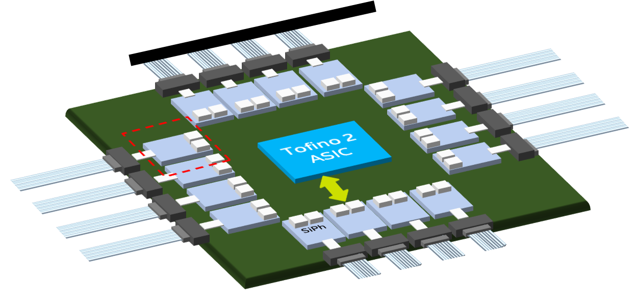
The advent of co-packaged optics has moved a step closer with Intel’s demonstration of a 12.8-terabit Ethernet switch chip with optical input-output (I/O).
The design couples a Barefoot Tofino 2 switch chip to up to 16 optical ‘tiles’ – each tile, a 1.6-terabit silicon photonics die – for a total I/O of 25.6 terabits.
“It’s an easy upgrade to add our next-generation 25.6-terabit [switch chip] which is coming shortly,” says Ed Doe, Intel’s vice president, connectivity group, general manager, Barefoot division.
Intel acquired switch-chip maker, Barefoot, seven months ago after which it started the co-packaging optics project.
Intel also revealed that it is in the process of qualifying four new optical transceivers – a 400Gbase-DR4, a 200-gigabit FR4, a 100-gigabit FR1 and a 100Gbase-LR4 – to add to its portfolio of 100-gigabit PSM4 and CWDM4 modules.
Urgency
Intel had planned to showcase the working co-packaged switch at the OFC conference and exhibition, held last week in San Diego. But after withdrawing from the show due to the Coronavirus outbreak, Intel has continued to demonstrate the working co-packaged switch at its offices in Santa Clara.

“We have some visionaries of the industry coming through and being very excited, making comments like: ‘This is an important milestone’,” says Hong Hou, corporate vice president, general manager, silicon photonics product division at Intel.
“There are a lot of doubts still [about co-packaged optics], in the reliability, the serviceability, time-to-market, and the right intercept point [when it will be needed]: is it 25-, 51- or 102-terabit switch chips?” says Hou. “But no one says this is not going to happen.”
If the timing for co-packaged optics remains uncertain, why the urgency?
“There has been a lot of doubters as to whether it is possible,” says Doe. “We had to show that this was feasible and more than just a demo.”
Intel has also been accumulating IP from its co-packaging work. Topics include the development of a silicon-photonics ring modulator, ensuring optical stability and signal integrity, 3D packaging, and passive optical alignment. Intel has also developed a fault-tolerant design that adds a spare laser to each tile to ensure continued working should the first laser fail.
“We can diagnose which laser is the source of the problem, and we have a redundant laser for each channel,” says Hou. “So instead of 16 lasers we have 32 functional lasers but, at any one time, only half are used.”
Co-packaged optics
Ethernet switches connected in the data centre currently use pluggable optics. The switch chip resides on a printed circuit board (PCB) and is interfaced to the pluggable modules via electrical traces.
But given that the capacity of the Ethernet switch ICs is doubling every two years, the power consumption of the I/O continues to rise yet the power delivered to a data centre is limited. Accordingly, solutions that ensure a doubling of switch speed but do not increase the power consumed are required.
One option is embedded optics such as the COBO initiative. Here, optics are moved from the switch’s faceplate onto the PCB, closer to the switch chip. This shortens the electrical traces while overcoming the capacity limitations of the number of pluggable modules that can be fitted onto the switch’s faceplate. Freeing up the faceplate by removing pluggables also improves airflow to cool the switch.
The second, more ambitious approach is co-packaged optics where optics are combined with the switch ASIC in the one package.
Co-packaged optics can increase the overall I/O on and off the switch chip, something that embedded optics doesn’t address. And placing the optics next to the ASIC, the drive requirements of the high-speed serialiser-deserialisers (serdes) is simplified.
Meanwhile, pluggable optics continue to advance in the form factors used and their speeds as well as developments such as fly-over cables that lower the loss connecting the switch IC to the front-panel pluggables.
In turn, certain hyperscalers are not convinced about co-packaged optics.
Microsoft and Facebook announced last year the formation of the Co-Packaged Optics (CPO) Collaboration to help guide the industry to develop the elements needed for packaging optics. But Google and Alibaba said at OFC that they prefer the flexibility and ease of maintenance of pluggables.
Data centre trends
The data centre is a key market for Intel which sells high-end server microprocessors, switch ICs, FPGAs and optical transceivers.
Large-scale data centres deploy 100,000 servers, 50,000 switches and over one million optical modules. And a million pluggable modules equate to $150M to $250M of potential revenue, says Intel.

“One item that is understated is the [2:1] ratio of servers to switches,” says Doe. “We have seen a trend in recent years where the layers of switching in data centres have increased significantly.”
One reason for more switching layers is that traffic over-subscription is no longer used. With top-of-rack switches, a 3:1 over-subscription was common which limited the switch’s uplink bandwidth needed.
However, the changing nature of the computational workloads now requires that any server can talk to any other server.
“You can’t afford to have any over-subscription at any layer in the network,” says Doe. “As a result, you need to have a lot more bandwidth: an equal amount of downlink bandwidth to uplink bandwidth.”
Another factor that has increased the data centre’s switch layer count is the replacement of chassis switches with disaggregated pizza boxes. Typically, a chassis switch encompasses three layers of switching.
“Disaggregation is a factor but the big one is the 1:1 [uplink-downlink bandwidth] ratio, not just at the top-of-rack switch but all the way through,” says Doe. “They [the hyperscalers] want to have uniform bandwidth throughout the entire data centre.”
Tofino switch IC
Barefoot has two families of Tofino chips. The first-generation Tofino devices have a switching capacity ranging from 1.2 to 6.4 terabits and are implemented using a 16nm CMOS process. The Tofino 2 devices, implemented using a 7nm CMOS IC, range from 4 terabits to 12.8 terabits.
“What we having coming soon is the Tofino next-generation which will go to both 25 terabits and 51 terabits,” says Doe.
Intel is not discussing future products but Doe hints that both switch ICs will be announced jointly rather than the typical two-year delay between successive generations of switch IC. This also explains the urgency of the company’s co-packaging work.
The 12.8-terabit Tofino 2 chip comprises the switch core dies and four electrical I/O tiles that house the device’s serdes.
“The benefit of the tile design is that it allows us to easily swap the tiles for higher-speed serdes – 112 gigabit-per-second (Gbps) – once they become available,” says Doe. And switching the tiles to optical was already envisaged by Barefoot.
Optical tile
Intel’s 1.6-terabit silicon-photonics tile includes two integrated lasers (active and spare), a ring modulator, an integrated modulator driver, and receiver circuitry. “We also have on-chip a v-groove which allows for passive optical alignment,” says Hou.
Each tile implements the equivalent of four 400GBASE-DR4s. The 500m-reach DR4 comprises four 100-gigabit channels, each sent over single-mode fibre.
“This is a standards-based interface,” says Robert Blum, Intel’s director of strategic marketing and business development, as the switch chip must interact with standard-based optics.
The switch chip and the tiles sit on an interposer. Having an interposer will enable different tiles and different system-on-chips to be used in future.
Hou says that having the laser integrated with the tile saves power. This contrasts with designs where the laser is external to the co-packaged design.
The argument for using an external laser is that it is remote from the switch chip which runs hot. But Hou says that the switch chip itself has efficient thermal management which the tile and its laser(s) can exploit. Each tile consumes 35W, he says.
As for laser reliability, Intel points to its optical modules that it has been selling since 2016 when it started selling the PSM4.
Hou claims Intel’s hybrid laser design, where the gain chip is separated from the cavity, is far more reliable than a III-V facet cavity.
“We have shipped over three million 100-gigabit transceivers, primarily the PSM4. The DPM [defects per million] is 28-30, about two orders of magnitude less than our closest competitor,” says Hou. “Eight out of ten times the cause of the failure of a transceiver is the laser, and nine out of ten times, the laser failure is due to a cavity problem.”
The module’s higher reliability reduces the maintenance needed, and enables data centre operators to offer more stringent service-level agreements, says Hou.
Intel says it will adopt wavelength-division multiplexing (WDM) to enable a 3.2-terabit tile which will be needed with the 51.2-terabit Tofino.
Switch platform
Intel’s 2-rack-unit (2RU) switch platform is a hybrid design: interfaced to the Tofino 2 are four tiles as well as fly-over cables to connect the chip to the front-panel pluggables.
“The hyperscalers are most interested in co-packaging but when you talk to enterprise equipment manufacturers, their customers may not have a fabric as complicated as that of the hyperscalers,” says Hou. “Bringing pluggables in there allows for a transition.”
The interposer design uses vertical plug-in connectors enabling a mix of optical and electrical interfaces “It is pretty easy, at the last minute, to [decide to] bring in 10 optical [interfaces] and six fly-over cables [to connect] to the pluggables,” says Hou.
“This is not like on-board optics,” adds Blum. “This [connector arrangement] is part of the multi-chip package, it doesn’t go through the PCB. It allows us to have [OIF-specified] XSR serdes and get the power savings.”
Intel expects its co-packaged design to deliver a 30 per cent power saving as well as a 25 to 30 per cent cost-saving. And now that it has a working platform, Hou expects more engagements with customers that seeking these benefits and its higher-bandwidth density.
“This can stimulate more discussions and drive an ecosystem formation around this technology,” concludes Hou.
See Part 2: Ranovus outlines its co-packaged optics plans.

Habana Labs unveils its AI processor plans
Start-up Habana Labs has developed a chip architecture that promises to speed up the execution of machine-learning tasks.
The Israeli start-up came out of secrecy in September to announce two artificial intelligence (AI) processor chips. One, dubbed Gaudi, is designed to tackle the training of large-scale neural networks. The chip will be available in 2019.
 Eitan MedinaGoya, the start-up’s second device, is an inference processor that implements the optimised, trained neural network.
The Goya chip is already in prospective customers’ labs undergoing evaluation, says Eitan Medina, Habana’s chief business officer.
Habana has just raised $75 million in a second round of funding, led by Intel Capital. Overall, the start-up has raised a total of $120 million in funding.
Deep learning
Deep learning in a key approach used to perform machine learning. To perform deep learning, use is made of an artificial neural network with many hidden layers. A hidden layer is a layer of nodes found between the neural network’s input and output layers.
To benefit from deep learning, the neural network must first be trained with representative data. This is an iterative and computationally-demanding process.
The computing resources used to train the largest AI jobs has been doubled every 3.5 months since 2012
Once trained, a neural network is ready to analyse data. Common examples where trained neural networks are used include image classification and for autonomous vehicles.
 Source: Habana Labs
Two types of silicon are used for deep learning: general-purpose server CPUs such as from Intel and graphics processing units (GPUs) from the likes of Nvidia.
Most of the growth has been in the training of neural networks and this is where Nvidia has done very well. Nvidia has a run rate close to $3 billion just building chips to do the training of neural networks, says Karl Freund, senior analyst, HPC and deep learning at Moor Insights & Strategy. “They own that market.”
Now custom AI processors are emerging from companies such as Habana that are looking to take business from Nvidia and exploit the emerging market for inference chips.
“Use of neural networks outside of the Super Seven [hyperscalers] is still a nascent market but it could be potentially a $20 billion market in the next 10 years,” says Freund. “Unlike in training where you have a very strong incumbent, in inference - which could be a potentially larger market - there is no incumbent.”
This is where many new chip entrants are focussed. After all, it is a lot easier to go after an emerging market than to displace a strong competitor such as Nvidia, says Freund, who adds that Nvidia has its own inference hardware but it is suited to solving really difficult problems such as autonomous vehicles.
“For any new processor architecture to have any justification, it needs to be significantly better than previous ones,” says Medina.
Habana cites the ResNet-50 image classification algorithm to highlight its silicon’s merits. ResNet-50 refers to a 50-layer neural network that makes use of a technique called residual learning that improves the efficacy of image classification.
Habana’s Goya HL-1000 processor can classify 15,000 images-per-second using ResNet-50 while Nvidia’s V100 GPU classifies 2,657and Intel’s dual-socket Platinum 8180 CPU achieves 1225 images-per-second.
“What we have architected is fundamentally better than CPUs and GPUs in terms of processing performance and the processing-power factor,” says Medina.
“Habana appears to be one of the first start-ups to bring an AI accelerator to the market, that is, to actually deliver a product for sale,” says Linley Gwennap, president and principal analyst of The Linley Group.
Both Habana and start-up Graphcore expect to have final products for sale this year, he says, while Wave Computing, another start-up, expects to enter production early next year.
“It is also impressive that Habana is reporting 5-6x better performance than Nvidia, whereas Graphcore’s lead is less than 2x,” says Gwennap. “Graphcore focuses on training, however, whereas the Goya chip is for inference.”
Habana appears to be one of the first start-ups to bring an AI accelerator to the market
Gaudi training processor
Habana’s Gaudi chip is a neural-network training processor. Once trained, the neural network is optimised and loaded into the inference chip such as Habana’s Goya to implement what has been learnt.
“The process of getting to a trained model involves a very different compute, scale-out and power-envelopment environment to that of inference,” says Medina.
To put this in perspective, the computing resources used to train the largest AI jobs has been doubled every 3.5 months since 2012. The finding, from AI research company OpenAI, means that the computing power being employed now has grown by over one million times since 2012.
Habana remains secretive about the details of its chips. It has said that the 16nm CMOS Gaudi chip can scale to thousands of units and that each device will have 2 terabits of input-output (I/O). This contrasts with GPUs used for training that do have scaling issues, it says.
First, GPUs are expensive and power-hungry devices. The data set used for training such as for image classification needs to be split across the GPUs. If the number of images - the batch size - given to each one is too large, the training model may not converge. If the model doesn't converge, the neural network will not learn to do its job.
In turn, reducing the batch size affects the overall throughput. “GPUs and CPUs want you to feed them with a lot of data to increase throughput,” says Medina.
Habana says that unlike GPUs, its training processor’s performance will scale with the number of devices used.
“We will show with the Gaudi that we can scale performance linearly,” says Medina. “Training jobs will finish faster and models could be much deeper and more complex.”
 The Goya IC architecture. Habana says this is a general representation of the chip and what is shown is not the actual number of tensor processor cores (TPCs). Source: Habana Labs
Goya inference processor
The Goya processor comprises multiple tensor processor cores (TPCs), see diagram. Habana is not saying how many but each TPC is capable of processing vectors and matrices efficiently using several data types - eight-, 16- and 32-bit signed and unsigned integers and 32-bit floating point. To achieve this, the architecture used for the TPC is a very-long-instruction-word, (VLIW) single-instruction, multiple-data (SIMD) vector processor. Each TPC also has its own local memory.
Other on-chip hardware blocks include a general-purpose engine (GEMM), shared memory, an interface to external DDR4 SDRAM memory and support for PCI Express (PCIe) 4.0.
What we have architected is fundamentally better than CPUs and GPUs in terms of processing performance and the processing-power factor
Habana claims its inference chip has a key advantage when it comes to latency, the time it takes for the inference chip to deliver its answer.
Latency too is a function of the batch size - the number of jobs - presented to the device. Being able to pool jobs presented to the chip is a benefit but not if it exceeds the latency required.
“If you listen to what Google says about real-time applications, to meet the 99th percentile of real-time user interaction, they need the inference to be accelerated to under 7 milliseconds,” says Medina. “Microsoft also says that latency is incredibly important and that is why they can’t use a batch size of 64.”
Habana and other entrants are going after applications where their AI processors are efficient at real-time tasks with a batch size of one. “Everyone is focussing on what Nvidia can’t do well so they are building inference chips that do very well with low batch sizes,” says Freund.
Having a low-latency device not only will enable all sorts of real-time applications but will also allow a data centre operator to rent out the AI processor to multiple customers, knowing what the latency will be for each job.
“This will generate more revenue and lower the cost of AI,” says Medina.
AI PCIe cards
Habana is offering two PCIe 4.0 card versions of its Goya chip: one being one-slot wide and the second being double width. This is to conform to some customers that already use platforms with double-width GPU cards.
Habana’s PCIe 4.0 card includes the Goya chip and external memory and consumes around 100W, the majority of the power consumed by the inference chip.
The card’s PCIe 4.0 interface has 16 lanes (x16) but nearly all the workloads can manage with a single lane.
“The x16 is in case you go for more complicated topologies where you can split the model between adjacent cards and then we need to pass information between our processors,” says Medina.
Here, a PCIe switch chip would be put on the motherboard to enable the communications between the Goya processors.
Do start-ups have a sustainable architectural roadmap that offers innovation beyond just such single-cycle operations?
Applications
Habana has developed demonstrations of four common applications to run on the Goya cards. These include image classification, machine translation, recommendations, and the classification of text known as sentiment analysis.
The four were chosen as potential customers want to see these working. “If they are going to buy your hardware for inference, they want to make sure it can deal with any topology they come up with in future,” says Medina.
Habana says it is already engaged with customers other than the largest data centre operators. And with time, the start-up expects to develop inference chips with tailored I/O to address dedicated applications such as autonomous vehicles.
There are also other markets emerging beside data centres and self-driving cars.
“Mythic, for example, targets security cameras while other start-ups offer IP cores, and some target the Internet of Things and other low-cost applications,” says Gwennap. “Eventually, most processors will have some sort of AI accelerator built-in, so there are many different opportunities for this technology.”
Start-up challenge
The challenge facing all the AI processor start-ups, says Freund, is doing more thandeveloping an architecture that can do a multiply-accumulate operation in a single processor clock cycle, and not just with numbers but withn-dimensional matrices.
“That is really hard but eventually - give or take a year - everyone will figure it out,” says Freund.
The question for the start-ups is: do they have a sustainable architectural roadmap that offers innovation beyond just such single-cycle operations?
“What architecturally are you able to do beyond that to avoid being crushed by Nvidia, and if not Nvidia then Intel because they haven't finished yet,” says Freund.
This is what all these start-ups are going to struggle with whereas Nvidia has 10,000 engineers figuring it out, he warns.
Article updated on Nov 16 to report the latest Series B funding.
Intel targets 5G fronthaul with a 100G CWDM4 module
- Intel announced at ECOC that it is sampling a 10km extended temperature range 100-gigabit CWDM4 optical module for 5G fronthaul.
- Another announced pluggable module pursued by Intel is the 400 Gigabit Ethernet (GbE) parallel fibre DR4 standard.
- Intel, a backer of the CWDM8 MSA, says the 8-wavelength 400-gigabit module will not be in production before 2020.
Intel has expanded its portfolio of silicon photonics-based optical modules to address 5G mobile fronthaul and 400GbE.
 Robert BlumAt the European Conference on Optical Communication (ECOC) being held in Rome this week, Intel announced it is sampling a 100-gigabit CWDM4 module in a QSFP form factor for wireless fronthaul applications.
The CWDM4 module has an extended temperature range, -20°C to +85°C, and a 10km reach.
“The final samples are available now and [the product] will go into production in the first quarter of 2019,” says Robert Blum, director of strategic marketing and business development at Intel’s silicon photonics product division.
Intel also announced it will support the 400GBASE-DR4, the IEEE’s 400 GbE standard that uses four parallel fibres for transmit and four for the receive path, each carrying a 100-gigabit 4-level pulse amplitude modulation (PAM-4) signal.
5G wireless
5G wireless will be used for a variety of applications. Already this year the first 5G fixed and mobile wireless services are expected to be launched. 5G will also support massive Internet of Things (IoT) deployments as well as ultra-low latency applications.
The next-generation wireless standard uses new spectrum that includes millimetre wave spectrum in the 24GHz to 40GHz region. Such higher frequency bands will drive small-cell deployments.
5G’s use of new spectrum, small cells and advanced air interface techniques such as multiple input, multiple output (MIMO) antenna technology is what will enable its greater data speeds and vastly expanded capacity compared to the current LTE cellular standard.
 Source: Intel.
The 5G wireless standard will also drive greater fibre deployment at the network edge. And it is here where mobile fronthaul plays a role, linking the remote radio heads at the antennas with the centralised baseband controllers at the central office (see diagram). Such fronthaul links will use 25-gigabit and 100-gigabit links. “We have multiple customers that are excited about the 100-gigabit CWDM4 for these applications,” says Blum
Intel expects demand for 25-gigabit and 100-gigabit transceivers for mobile fronthaul to begin in 2019.
Intel is now producing over one million PSM4 and CWDM4 modules a year
Client-side modules
Intel entered the optical module market with its silicon photonics technology in 2016 with a 100-gigabit PSM4 module, quickly followed by a 100-gigabit CWDM4 module. Intel is now producing over one million PSM4 and CWDM4 modules a year.
Intel will provide customers with 400-gigabit DR4 samples in the final quarter of 2018 with production starting in the second half of 2019. This is when Intel says large-scale data centre operators will require 400 gigabits.
“The initial demand in hyperscale data centres for 400 gigabits will not be for duplex [fibre] but parallel fibre,” says Blum. “So we expect the DR4 to go to volume first and that is why we are announcing the product at ECOC.”
Intel says the advantages of its silicon photonics approach have already been demonstrated with its 100-gigabit PSM4 module. One is the optical performance resulting from the company’s heterogeneous integration technique combining indium-phosphide lasers with silicon photonics modulators on the one chip. Another advantage is scale using Intel’s 300mm wafer-scale manufacturing.
Intel says demand for the 500m-reach DR4 module to go hand-in-hand with that for the 100-gigabit single- wavelength DR1, given how the DR4 will also be used in breakout mode to interface with four DR1 modules.
“We don’t see the DR1 standard competing or replacing 100-gigabit CWDM4,” says Blum. “The 100-gigabit CWDM4 is now mature and at a very attractive price point.”
Intel is a leading proponent of the CWDM8 MSA, an optical module design based on eight wavelengths, each a 50 gigabit-per-second (Gbps) non-return-to-zero (NRZ) signal. The CWDM8 MSA was created to fast-track 400 gigabit interfaces by avoiding the wait for 100-gigabit PAM-4 silicon.
When the CWDM8 MSA was launched in 2017, the initial schedule was to deploy the module by the end of this year. Intel also demonstrated the module working at the OFC show held in March.
Now, Intel expects production of the CWDM8 in 2020 and, by then, other four-wavelength solutions using 100-gigabit PAM-4 silicon such as the 400G-FR4 MSA will be available.
“We just have to see what the use case will be and what the timing will be for the CWDM8’s deployment,” says Blum.
The CWDM8 MSA avoids PAM-4 to fast-track 400G
Another multi-source agreement (MSA) group has been created to speed up the market introduction of 400-gigabit client-side optical interfaces.
The CWDM8 MSA is described by its founding members as a pragmatic approach to provide 400-gigabit modules in time for the emergence of next-generation switches next year. The CWDM8 MSA was announced at the ECOC show held in Gothenburg last week.
Robert BlumThe eight-wavelength coarse wavelength-division multiplexing (CWDM) MSA is being promoted as a low-cost alternative to the IEEE 803.3bs 400 Gigabit Ethernet Task Force’s 400-gigabit eight-wavelength specifications, and less risky than the newly launched 100G Lambda MSA specifications based on four 100-gigabit wavelengths for 400 gigabit.
“The 100G Lambda has merits and we are also part of that MSA,” says Robert Blum, director of strategic marketing and business development at Intel’s silicon photonics product division. “We just feel the time to get to 100-gigabit-per-lambda is really when you get to 800 Gigabit Ethernet.”
Intel is one of the 11 founding companies of the CWDM8 MSA.
Specification
The CWDM8 MSA will develop specifications for 2km and 10km links. The MSA uses wavelengths spaced 20nm apart. As a result, unlike the IEEE’s 400GBASE-FR8 and 400GBASE-LR8 that use the tightly-spaced LAN-WDM wavelength scheme, no temperature control of the lasers is required. “It is just like the CWDM4 but you add four more wavelengths,” says Blum.
The CWDM8 MSA also differs from the IEEE specifications and the 100G Lambda MSA in that it does not use 4-level pulse-amplitude modulation (PAM-4). Instead, 50-gigabit non-return-to-zero (NRZ) signalling is used for each of the eight wavelengths.
The MSA will use the standard CDAUI-8 8x50-gigabit PAM-4 electrical interface. Accordingly, a retimer chip will be required inside the module to translate the input 50-gigabit PAM electrical signal to 50-gigabit NRZ. According to Intel, several companies are developing such a chip.
When we looked at what is available and how to do an optical interface, there was no good solution that would allow us to meet those timelines
Benefits
Customers are telling Intel that they need 400-gigabit duplex-fibre optical modules early next year and that they want to have them in production by the end of 2018.
“When we looked at what is available and how to do an optical interface, there was no good solution that would allow us to meet those timelines, fit the power budget of the QSFP-DD [module] and be at the cost points required for data centre deployment,” says Blum.
An 8x50-gigabit NRZ approach is seen as a pragmatic solution to meet these requirements.
No PAM-4 physical layer DSP chip is needed since NRZ is used. The link budget is significantly better compared to using PAM-4 modulation. And there is a time-to-market advantage since the technologies used for the CWDM8 are already proven.
We just think it [100-gigabit PAM4] is going to take longer than some people believe
This is not the case for the emerging 100-gigabit-per-wavelength MSA that uses 50-gigabaud PAM-4. “PAM-4 makes a lot of sense on the electrical side, a low-bandwidth [25 gigabaud], high signal-to-noise ratio link, but it is not the ideal when you have high bandwidth on the optical components [50 gigabaud] and you have a lot of noise,” says Blum.
One-hundred-gigabit-per-wavelength will be needed for the optical path, says Blum, but for 800 Gigabit Ethernet with its eight electrical channels and eight optical ones. “We just think it [100-gigabit PAM4] is going to take longer than some people believe.” Meanwhile, the CWDM8 is the best approach to meet market demand for a 400-gigabit duplex interfaces to support next-generation data centre switches expected next year, says Blum.
The founding members of the CWDM8 MSA include chip and optical component players as well as switch system makers. Unlike the 100G Lambda MSA, no larger-scale data centre operators have joined the MSA.
The members are Accton, Barefoot Networks, Credo Semiconductor, Hisense, Innovium, Intel, MACOM, Mellanox, Neophotonics and Rockley Photonics.
Reflections on OFC 2017
Mood, technologies, notable announcements - just what are the metrics to judge the OFC 2017 show held in Los Angeles last week?
It was the first show I had attended in several years and the most obvious changes were how natural the presence of the internet content providers now is alongside the telecom operators, as well as systems vendors exhibiting at the show. Chip companies, while also present, were fewer than before.
 Source: OSA
Another impression were the latest buzz terms: 5G, the Internet of Things and virtual reality-augmented reality. Certain of these technologies are more concrete than others, but their repeated mention suggests a consensus that the topics are real enough to impact optical components and networking.
It could be argued that OFC 2017 was the year when 400 Gigabit Ethernet became a reality
The importance of 5G needs no explanation while the more diffuse IoT is expected to drive networking with the huge amounts of data it will generate. But what are people seeing about virtual reality-augmented reality that merits inclusion alongside 5G and IoT?
Another change is the spread of data rates. No longer does one rate represent the theme of an OFC such as 40 Gigabits or 100 Gigabits. It could be argued that OFC 2017 was the year when 400 Gigabit Ethernet became a reality but there is now a mix of relevant rates such as 25, 50, 200 and 600 gigabits.
Highlights
There were several highlights at the show. One was listening to Jiajin Gao, deputy general manager at China Mobile Technology, open the OIDA Executive Forum event by discussing the changes taking place in the operator's network. Gao started by outlining the history of China Mobile's network before detailing the huge growth in ports at different points in the network over the last two years. He then outlined China Mobile's ambitious rollout of new technologies this year and next.
China's main three operators have 4G and FTTx subscriber numbers that dwarf the rest of the world. Will 2017 eventually be seen as the year when the Chinese operators first became leaders in telecom networking and technologies?
The Executive Forum concluded with an interesting fireside discussion about whether the current optical market growth is sustainable. The consensus among representatives from Huawei, Hisense, Oclaro and Macom was that it is; that the market is more varied and stable this time compared to the boom and bust of 1999-2001. As Macom’s Preetinder Virk put it: "The future has nothing to do with the past". Meanwhile, Huawei’s Jeffrey Gao still expects strong demand in China for 100 gigabits in 2017 even if growth is less strong than in 2016. He also expects the second quarter this year to pick up compared to a relatively weak first quarter.
OFC 2017 also made the news with an announcement that signals industry change: Ciena's decision to share its WaveLogic Ai coherent DSP technology with optical module vendors Lumentum, Oclaro and NeoPhotonics.
The announcement can be viewed several ways. One is that the initiative is a response to the success of Acacia as a supplier of coherent modules and coherent DSP technology. System vendors designed their own coherent DSP-ASICs to differentiate their optical networking gear. This still holds true but the deal reflects how the progress of merchant line-side optics from the likes of Acacia is progressing and squeezing the scope for differentiation.
The deal is also a smart strategic move by Ciena which, through its optical module partners, will address new markets and generate revenues as its partners start to sell modules using the WaveLogic Ai. The deal also has a first-mover advantage. Other systems vendors may now decide to offer their coherent DSPs to the marketplace but Ciena has partnerships with three leading optical module makers and is working with them on future DSP developments for pluggable modules.
The deal also raises wider questions as to the role of differentiated hardware and whether it is subtly changing in the era of network function virtualisation, or whether it is a reflection of the way companies are now collaborating with each other in open hardware developments like the Telecom Infra Project and the Open ROADM MSA.
Another prominent issue at the show is the debate as to whether there is room for 200 Gigabit Ethernet modules or whether the industry is best served by going straight from 100 to 400 Gigabit Ethernet.
Facebook and Microsoft say they will go straight to 400 gigabits. Cisco agrees, arguing that developing an interim 200 Gigabit Ethernet interface does not justify the investment. In contrast, Finisar argues that 200 Gigabit Ethernet has a compelling cost-per-bit performance and that it will supply customers that want it. Google supported 200 gigabits at last year’s OFC.
Silicon photonics
Silicon photonics was one topic of interest at the show and in particular how the technology continues to evolve. Based on the evidence at OFC, silicon photonics continues to progress but there were no significant developments since our book (co-written with Daryl Inniss) on silicon photonics was published late last year.
One of the pleasures of OFC is being briefed by key companies in rapid succession. Intel demonstrated at its booth its silicon photonics products including its CWDM4 module which will be generally available by mid-year. Intel also demonstrated a 10km 4WDM module. The 4WDM MSA, created last year, is developing a 10km reach variant based on the CWDM4, as well as 20km and 40km based designs.
Meanwhile, Ranovus announced its 200-gigabit CFP2 module based on its quantum dot laser and silicon photonics ring resonator technologies with a reach approaching 100km. The 200 gigabit is achieved using 28Gbaud optics and PAM-4.
Elenion Technologies made several announcements including the availability of its monolithically integrated coherent modulator receiver after detailing it was already supplying a 200 gigabit CFP2-ACO to Coriant. The company was also demonstrating on-board optics and, working with Cavium, announced a reference architecture to link network interface cards and switching ICs in the data centre.
I visited Elenion Technologies in a hotel suite adjacent to the conference centre. One of the rooms had enough test equipment and boards to resemble a lab; a lab with a breathtaking view of the hills around Los Angeles. As I arrived, one company was leaving and as I left another well-known company was arriving. Elenion was using the suite to demonstrate its technologies with meetings continuing long after the exhibition hall had closed.
Two other silicon photonics start-ups at the show were Ayar Labs and Rockley Photonics.
Ayar Labs in developing a silicon photonics chip based on a "zero touch" CMOS process that will sit right next to complex ASICs and interface to network interface cards. The first chip will support 3.2 terabits of capacity. The advantage of the CMOS-based silicon photonics design is the ability to operate at high temperatures.
Ayar Labs is using the technology to address the high-bandwidth, low-latency needs of the high-performance computing market, with the company expecting the technology to eventually be adopted in large-scale data centres.
Rockley Photonics shared more details as to what it is doing as well as its business model but it is still to unveil its first products.
The company has developed silicon photonics technology that will co-package optics alongside ASIC chips. The result will be packaged devices with fibre-based input-output offering terabit data rates.
Rockley also talked about licensing the technology for a range of applications involving complex ICs including coherent designs, not just for switching architectures in the data centre that it has discussed up till now. Rockley says its first product will be sampling in the coming months.
Looking ahead
On the plane back from OFC I was reading The Undoing Project by Michael Lewis about the psychologists Danny Kahneman and Amos Tversky and their insights into human thinking.
The book describes the tendency of people to take observed facts, neglecting the many facts that are missed or could not be seen, and make them fit a confident-sounding story. Or, as the late Amos Tversky put it: "All too often, we find ourselves unable to predict what will happen; yet after the fact, we explain what did happen with a great deal of confidence. This 'ability' to explain that which we cannot predict, even in the absence of any additional information, represents an important, though subtle, flaw in our reasoning."
So, what to expect at OFC 2018? More of the same and perhaps a bombshell or two. Or to put it another way, greater unpredictability based on the impression at OFC 2017 of an industry experiencing an increasing pace of change.
Heterogeneous integration comes of age
Silicon photonics luminaries series
Interview 7: Professor John Bowers
August has been a notable month for John Bowers.
Juniper Networks announced its intention to acquire Aurrion, the US silicon photonics start-up that Bowers co-founded with Alexander Fang. And Intel, a company Bowers worked with on a hybrid integration laser-bonding technique, unveiled its first 100-gigabit silicon photonics transceivers.
 Professor John BowersBower, a professor in the Department of Electrical and Computer Engineering at the University of California, Santa Barbara (UCSB), first started working in photonics in 1981 while at AT&T Bell Labs.
When he became interested in silicon photonics, it still lacked a good modulator and laser. "If you don't have a laser and a modulator, or a directly modulated laser, it is not a very interesting chip,” says Bowers. "So I started thinking how to do that."
Bowers contacted Mario Paniccia, who headed Intel’s silicon photonics programme at the time, and said: “What if we can integrate a laser? I think there is a good way to do it.” The resulting approach, known as heterogeneous integration, is one that both Intel and Aurrion embraced and since developed.
This is a key Bowers trait, says Aurrion co-founder, Fang: he just knows what problems to work on.
"John came up with the concept of the hybrid laser very early on," says Fang. "Recall that, at that time, silicon photonics was viewed as nothing more than people making plasma-effect phase shifters and simple passive devices. John just cut to the chase and went after combining III-V materials with silicon."
If you look at the major companies with strong photonics activities, you’ll find a leader in that group that was developed under John’s training
Fang also highlights Bowers' management skills. “John can pick players and run teams,” says Fang, who describes himself as one of those privileged to graduate out of Bowers’ research group at UCSB.
“You find yourself in an environment where John picks a team of sharp folk with complementary skills and domain expertise to solve a problem that John determines as important and has some insight on how to solve it,” says Fang. “If we look like we are going to drive off the road, he nudges with a good mix of insight, fear, and humour.”
It has resulted in some of the best trained independent thinkers and leaders in the industry, says Fang: “If you look at the major companies with strong photonics activities, you’ll find a leader in that group that was developed under John’s training”.
Silicon photonics
Bowers defines silicon photonics as photonic devices on a silicon substrate fabricated in a CMOS facility.
“Silicon photonics is not about using silicon for everything; that misses the point,” says Bowers. “The key element is using silicon as a substrate - 12-inch wafers and not 2- or 3-inch wafers - and having all the process capability a modern silicon CMOS facility brings.” These capabilities include not just wafer processing but also advanced testing and packaging.
The world is about to change and I don't think people have quite figured that out
“If you go to an advanced packaging house, they don't do 6-inch wafers and I don't know of indium phosphide and gallium arsenide wafers larger than 6 inches,” says Bowers. “The only solution is to go to silicon; that is the revolution that hasn't happened yet but it is happening now.”
Bowers adds that everything Aurrion does, there is automated test along the way. "And I think you have others; Luxtera has done a great job as well at wafer-level test and packaging," he says. "The world is about to change and I don't think people have quite figured that out."
Working with Intel was an eye-opener for Bowers, especially the process controls it applies to chip-making.
“They worry about distributions and yields, and it is clear why there are seven billion transistors on a chip and that chip will yield,” says Bowers. “When you apply that to photonics, it will take it to a whole new level.” Indeed, Bowers foresees photonics transfering to silicon.
Bowers highlights the fairly complex chips now being developed using silicon photonics.
“We have done a 2D scanner - a 32-element phased array - something one could never do in optics unless it was integrated all on one chip,” he says. The phased-array chip comprises 160 elements and is physically quite large.
This is another benefit of using 12-inch silicon wafers and fabricating the circuits in a CMOS facility. “You are not going to cost-effectively do that in indium phosphide, which I've worked on for the last 30 years,” says Bowers.
Another complex device developed at UCSB is a 2.54-terabit network-on-a-chip. “This is a larger capacity than anyone has done on any substrate,” he says.
Infinera’s latest photonic integrated circuit (PIC), for example, has a transport capacity of up to 2.4 terabit-per-second. That said, Bowers stresses that the network-on-a-chip is a research presentation while Infinera’s PIC is a commercial device.
Heterogeneous integration
Heterogeneous integration involves bonding materials such as III-V compounds onto silicon.
Bowers first worked on III-V bonding with HP to make longer wavelength - 1310nm and 1550nm - VCSELs. “We had been bonding indium phosphide and gallium arsenide to solve a fundamental problem that indium phosphide does not make good mirrors,” he says. “So I was pretty confident we could bond III-V to silicon to add gain to silicon photonics to then add all the laser capability.”
Bonding to silicon is attractive as it enables the integration of optical features that haven't been widely integrated onto any other platform, says Bowers. These include not only lasers but other active devices such as modulators and photo-detectors, as well as passive functions such as isolators and circulators.
One concern raised about heterogeneous integration and the use of III-V materials is the risk of contamination of a CMOS fabrication line.
Bowers points out that the approached used does not impact the front end of the fabrication, where silicon wafers are etched and waveguides formed. The III-V material is bonded to the wafer at the fab’s back end, the stage where metallisation occurs when making a CMOS chip.
The leading chipmakers are also experimenting with III-V materials to create faster digital devices due to their higher electron mobility. “This is part of the natural evolution of CMOS,” he says. It remains unclear if this will be adopted, but it is possible that a 5nm CMOS node will use indium phosphide.
“All the CMOS houses are doing lots of work on III-V and silicon,” says Bowers. “They have figured out how to control that contamination issue.”
New capabilities
Bowers and his team have already demonstrated the integration of new optical functions on silicon.
“Neither silicon nor indium phosphide has an isolator and one always has to use an external YIG (yttrium iron garnet) isolator to reduce the reflection sensitivity of things like widely tunable lasers,” says Bower.
His team has developed a way to bond a YIG onto silicon using the same techniques it uses for bonding III-V materials. The result is an integrated isolator device with 32dB isolation and a 2dB insertion loss, a level of performance matching those of discrete isolators.
Incorporating such functionality onto silicon creates new possibilities. “We have a paper coming out that features a 6-port circulator,” says Bowers. “It is not a tool that the community can use yet because it has never been made before but we can do that on silicon now,” he says. “That is a good new capability.”
Superior performance
Bowers stresses that heterogeneous integration can also result in optical performance superior to a III-V design alone. He cites as an example how using a silicon nitride waveguide, with its lower loss that indium phosphide or gallium arsenide, can create high-quality Q-resonators.
A Q-resonator can be viewed as a form of filter. Bowers' group have demonstrated one with a Q of 80 million. “That makes it very sensitive to a variety of things,” he says. One example is for sensors, using a Q resonator with a laser and detector to form a spectrometer.
His researchers have also integrated the Q resonator with a laser to make a widely tunable device that has a very narrow line-width: some 40kHz wide. This is a narrower than the line-width of commercially-available tunable lasers and exceeds what can be done with indium phosphide alone, he says.
Challenges
Bowers, like other silicon photonics luminaries, highlights the issues of automated packaging and automated testing, as important challenges facing silicon photonics. “Taking 10,000s of transceivers and bringing all the advanced technology - not just processing but test and packaging - that are being developed for cell phones,” he says.
Too much of photonics today is based on gold boxes and expensive transceivers. “Where Aurrion and Intel are going is getting silicon photonics to the point where photonics will be ubiquitous, cheap and high yielding,” he says. This trend is even evident with his university work. The 400-element 2.54-terabit network-on-a-chip has very high laser yields, as are its passive yields, he says.
“So, effectively, what silicon photonics can do is going up very rapidly,“ says Bowers. “If you can put it in the hands of a real CMOS player like Intel or the companies that Aurrion uses, it is going to take photonics to a whole new area that people would not have thought possible in terms of complexity.”
Yet Bowers is also pragmatic. “It still takes time,” he says. “You can demonstrate an idea, but it takes time to make it viable commercially.”
He points to the recently announced switch from Oracle that uses mid-board optics. “That is a commercial product out there now,” he says. “But is it silicon photonics? No, it is VCSEL-based; that is the battle going on now.”
VCSELs have won the initial battle in the data centre but the amount of integration the technology can support is limited. Once designers move to wavelength-division multiplexing to get to higher capacities, where planar technology is required to combine and separate the different wavelengths efficiently, that is when silicon has an advantage, he says.
The battle at 100 gigabit between VCSELs and silicon photonics is also one that Bowers believes silicon photonics will eventually win. But at 400 gigabit and one terabit, there is no way to do that using VCSELs, he says.
Status
The real win for silicon photonics is when optics moves from transceivers at the edge of the board to mid-board and eventually are integrated with a chip in the same package, he says.
Advanced chips such as switch silicon for the data centre are running into an input-output problem. There are only so many 25 gigabit-per-second signals a chip can support. Each signal, sent down a trace on a printed circuit board, typically requires equalisation circuitry at each end and that consumes power.
Most of the photonics industry has focused on telecom and datacom, and justifiably so. The next big thing will happen in the area of sensors.
A large IC packaged as a ball grid array may have as many as 5,000 bumps (balls) that are interfaced to the printed circuit board. Using photonics can boost the overall bandwidth coming on and off the chip.
“With photonics, and in particular when we integrate the laser as well as the modulator, the world doesn't see it as a photonics chip, it's an electronics chip, it just turns out that some of those bumps are optical ones and they provide much more efficient transmission of data and at much lower power,” say Bowers. A 100 terabit of even a 1000 terabit - a petabit - switch chip then becomes possible. This is not possible electrically but it is possible by integrating photonics inside the package or on the chip itself, he says.
“That is the big win eventually and that is where we help electronics extend Moore’s law,” says Bowers.
And as silicon photonics matures, other applications will emerge - More than Moore’s law - like the use of photonics for sensors.
“Most of the photonics industry has focused on telecom and datacom, and justifiably so,” says Bowers. “The next big thing will happen in the area of sensors.”
Professor Bowers was interviewed before the Juniper Networks announcement
Intel's 100-gigabit silicon photonics move
Intel has unveiled two 100-gigabit optical modules for the data centre made using silicon photonics technology.
 Alexis Bjorlin
The PSM4 and CWDM4/CLR4 100-gigabit modules mark the first commercial application of a hybrid integration technique for silicon photonics, dubbed heterogeneous integration, that Intel has been developing for years.
Intel's 100-gigabit module announcement follows the news that Juniper Networks has entered into an agreement to acquire start-up, Aurrion, for $165 million. Aurrion is another silicon photonics player developing this hybrid integration technology for its products.
Hybrid integration
With heterogeneous integration, materials such as indium phosphide and gallium arsenide can be bonded to the silicon substrate before the 300mm wafer is processed to produce the optical circuit. Not only can lasers be added to silicon but other active devices such as modulators and photo-detectors as well as passive functions such as isolators and circulators.
There is no alignment needed; we align the laser with lithography
Intel is using the technique to integrate the laser as part of the 100-gigabit transceiver designs.
"Once we apply the light-emitting material down to the silicon base wafer, we define the laser in silicon," says Alexis Bjorlin, vice president and general manager, Intel Connectivity Group. “There is no alignment needed; we align the laser with lithography.”
Intel claims it gets the highest coupling efficiency between the laser and the optical waveguide and modulator because it is lithographically defined and requires no further alignment.
100-gigabit modules
Intel is already delivering the 100-gigabit PSM4 module. “First volume shipments are happening now,” says Bjorlin. Microsoft is one Internet content provider that is using Intel’s PSM4.
The chip company is also sampling a 100-gigabit CWDM4 module that also meets the more demanding CLR4 Alliance’s optical specification. The 100-gigabit CLR4 module can be used without forward-error correction hardware and is favoured for applications where latency is an issue such as high-performance computing.
Intel is not the first vendor to offer PSM4 modules, nor is it the first to use silicon photonics for such modules. Luxtera and Lumentum are shipping silicon photonics-based PSM4 modules, while STMicroelectronics is already supplying its PSM4 optical engine chip.
We are right on the cusp of the real 100-gigabit connectivity deployments
“Other vendors have been shipping PSM4 modules for years, including large quantities at 40 gigabit,” says Dale Murray, principal analyst at LightCounting Market Research. “Luxtera has the clear lead in silicon photonics-based PSM4 modules but a number of others are shipping them based on conventional optics.”
The PSM4 is implemented using four independent 25-gigabit channels sent over a single-mode ribbon fibre. Four fibres are used for transmission and four fibres for receive.
“The PSM4 configuration is an interesting design that allows one laser to be shared among four separate output fibres,” says Murray. “As Luxtera has shown, it is an effective and efficient way to make use of silicon photonics technology.”
The CWDM4 is also a 4x25-gigabit design but uses wavelength-division multiplexing and hence a single-mode fibre pair. The CWDM4 is a more complex design in that an optical multiplexer and demultiplexer are required and the four lasers operate at different wavelengths.
“While the PSM4 module does not break new ground, Intel’s implementation of WDM via silicon photonics in a CWDM4/CLR4 module could be more interesting in a low-cost QSFP28 module,” says Murray. WDM-based QSFP28 modules are shipping from a number of suppliers that are using conventional optics, he says.
Intel is yet to detail when it will start shipping the CWDM4/CLR4 module.
Market demand
Bjorlin says the PSM4 and the CWDM4/CLR4 will play a role in the data centre. There are applications where being able to break out 100-gigabit into 25-gigabit signals as offered by the PSM4 is useful, while other data centre operators prefer a duplex design due to the efficient use of fibre.
“We are right on the cusp of the real 100-gigabit connectivity deployments,” she says.
As for demand, Bjorlin expects equal demand for the two module types in the early phases: “Longer term, we will probably see more demand for the duplex solution”.
LightCounting says that 100-gigabit PSM4 modules took an early lead in the rollout of 100 Gigabit Ethernet, with VCSEL-based modules not far behind.
“Some are shipping CWDM4/CLR4 and we expect that market to ramp,” says Murray. “Microsoft and Amazon Web Services seem to like PSM4 modules while others want to stick with modules that can use duplex fibre.
 Source: Intel
Data centre switching
“One of the most compelling reasons to drive silicon photonics in the future is that it is an integratable platform,” says Bjorlin.
Switch silicon from the likes of Broadcom support 3.2 terabits of capacity but this will increase to 6.4 terabits by next year and 12.8 terabits using 4-level pulse amplitude modulation (PAM-4) signalling by 2018 (see chart). And by 2020, 25.6-terabit capacity switch chips are expected.
The demand for 100 gigabit is for pluggable modules that fit into the front panels of data center switches. But the market is evolving to 400-gigabit embedded optics that sit on the line card, she says, to enable these emerging higher-capacity switches. Intel is a member of the Consortium of On-Board Optics (COBO) initiative that is being led by Microsoft.
“When you get to 25.6-terabit switches, you start to have a real problem getting the electrical signals in and out of the switch chip,” says Bjorlin. This is where silicon photonics can play a role in the future by co-packaging the optics alongside the switch silicon.
“There will be a need for an integrated solution that affords the best power consumption, the best bandwidth-density that we can get and effectively position silicon photonics for optical I/O [input/output],” says Bjorlin. “Ultimately, that co-packaging is inevitable.”
Mario Paniccia: We are just at the beginning
 During that time, his Intel team had six silicon photonics papers published in the science journals, Nature and Nature Photonics, and held several world records - for the fastest modulator, first at 1 gigabit, then 10 gigabit and finally 40 gigabit, the first pulsed and continuous-wave Raman silicon laser, the first hybrid silicon laser working with The University of California, Santa Barbara, and the fastest silicon germanium photo-detector operating at 40 gigabit.
It got to the stage where Intel’s press relations department would come and ask what the team would be announcing in the coming months. “ 'Hey guys,' I said, 'it doesn't work that way ' ”.
Since leaving Intel last year, Paniccia has been working as a consultant and strategic advisor. He is now exploring opportunities for silicon photonics but in segments other than telecom and datacom.
“I didn't want to go into developing transceivers for other big companies and compete with my team's decade-plus of development; I spent 20 years at Intel,” he says.
Decade of development
Intel’s silicon photonics work originated in the testing of its microprocessors using a technique known as laser voltage probing. Infra-red light is applied to the back side of the silicon to make real-time measurements of the chip’s switching transistors.
For Paniccia, it raised the question: if it is possible to read transistor switching using light, can communications between silicon devices also be done optically? And can it be done in parallel to the silicon rather than using the back side of silicon?
In early 2000 Intel started working with academic Graham Reed, then at the University of Surrey, and described by Paniccia as one of the world leaders in silicon photonics devices. “We started with simple waveguides and it just progressed from there,” he says.
The Intel team set the target of developing a silicon modulator working at 1 gigahertz (GHz); at the time, the fastest silicon modulator operated at 10 megahertz. “Sometimes leadership is about pushing things out and putting a stake in the ground,” he says.
It was Intel’s achievement of a working 1GHz silicon modulator that led to the first paper in Nature. And by the time the paper was published, Intel had the modulator working at 2GHz. The work then progressed to developing a 10 gigabit-per-second (Gbps) modulator and then broadened to include developing other silicon photonics building-block devices that would be needed alongside the modulator – the hybrid silicon laser, the photo-detector and other passive devices needed for an integrated transmitter.
There is a difference between proving the technology works and making a business out of it
Once 10Gbps was achieved, the next milestone was 20Gbps and then 40Gbps. Once the building block devices achieved operation in excess of 40Gbps, Intel’s work turned to using these optical building blocks in integrated designs. This was the focus of the work between 2010 to 2012. Intel chose to develop a four-channel 40Gbps (4x10 gigabit) transceiver using four-wavelength coarse WDM which ended up working at 50Gbps (4x12.5 gigabit) and then, most recently, a 100Gbps transceiver.
He says the same Intel team is no longer talking about 50Gbps or 100Gbps but how to get multiple terabits coming out of a chip.
Status
Paniccia points out that in little more than a decade, the industry has gone from not knowing whether silicon could be used to make basic optical functions such as modulators and photo-detectors, to getting them to work at speeds in excess of 40Gbps. “I’d argue that today the performance is close to what you can get in III-V [compound semiconductors],” he says.
He believes silicon photonics is the technology of the future, it is just a question of when and where it is going to be applied: “There is a difference between proving the technology works and making a business out of it”.
In his mind, these are the challenges facing the industry: proving silicon photonics can be a viable commercial technology and determining the right places to apply it.
For Paniccia, the 100-gigabit market is a key market for silicon photonics. “I do think that 100 gigabit is where the intercept starts, and then silicon photonics becomes more prevalent as you go to 200 gigabit, 400 gigabit and 1 terabit,” he says.
So has silicon photonics achieved its tipping point?
Paniccia defines the tipping point for silicon photonics as when people start believing the technology is viable and are willing to invest. He cites the American Institute for Manufacturing Integrated Photonics (AIM Photonics) venture, the $610 million public and private funded initiative set up in 2015 to advance silicon photonics-based manufacturing. Other examples include the silicon photonics prototyping service coordinated by nano-electronics research institute imec in Belgium, and global chip-maker STMicroelectronics becoming a silicon photonics player having developed a 12-inch wafer manufacturing line.
Instead of one autonomous LIDAR system in a car, you could have 20 or 50 or 100 sprinkled throughout your vehicle
“All these are places where people not only see silicon photonics as viable but are investing significant funds to commercialise the technology,” says Paniccia. “There are numerous companies now selling commercialised silicon photonics, so I think the tipping point has passed.”
Another indicator that the tipping point has happened, he argues, is that people are not spending their effort and their money solely on developing the technology but are using CMOS processes to develop integrated products.
“Now people can say, I can take this process and build integrated devices,” he says. “And when I put it next to a DSP, or an FPGA, or control electronics or a switching chip, I can do things that you couldn't do next to bulky electronics or bulky photonics.”
It is this combination of silicon photonics with electronics that promises greater computing power, performance and lower power consumption, he says, a view shared by another silicon photonics luminary, Rockley Photonics CEO, Andrew Rickman.
Moreover, the opportunities for integrated photonics are not confined to telecom and datacom. “Optical testing systems for spectroscopy today is a big table of stuff - lasers, detectors modulators and filters,” says Paniccia. Now all these functions can be integrated on a chip for such applications as gas sensing, and the integrated photonics device can then be coupled with a wireless chip for Internet of Things applications.
The story is similar with autonomous vehicle systems that use light detection and ranging (LIDAR) technology. “These systems are huge, complicated, have a high power consumption, and have lots of lasers that are spinning around,” he says. “Now you can integrate that on a chip with no moving parts, and instead of one autonomous LIDAR system in a car, you could have 20 or 50 or 100 sprinkled throughout your vehicle”
Disruptive technology
Paniccia is uncomfortable referring to silicon photonics as a disruptive technology. He believes disruption is a term that is used too often.
Silicon photonics is a technology that opens up a lot of new possibilities, he says, as well as a new cost structure and the ability to produce components in large volume. But it doesn’t solve every problem.
The focus of the optical vendors is very much on cost. For markets such as the large-scale data centre, it is all about achieving the required performance at the right cost for the right application. Packaging and testing still account for a significant part of the device's overall cost and that cannot be forgotten, he says.
Paniccia thus expects silicon photonics to co-exist with the established technologies of indium phosphide and VCSELs in the near term.
“It is all about practical decisions based on price, performance and good-enough solutions,” he says, adding that silicon photonics has the opportunity to be the mass market solution and change the way one thinks about where photonics can be applied.
“Remember we are just at the beginning and it will be very exciting to see what the future holds.”
Altera’s 30 billion transistor FPGA
- The Stratix 10 features a routing architecture that doubles overall clock speed and core performance
- The programmable family supports the co-packaging of transceiver chips to enable custom FPGAs
- The Stratix 10 family supports up to 5.5 million logic elements
- Enhanced security features stop designs from being copied or tampered with
Altera has detailed its most powerful FPGA family to date. Two variants of the Stratix 10 family have been announced: 10 FPGAs and 10 system-on-chip (SoC) devices that include a quad-core 64-bit architecture Cortex-A53 ARM processor alongside the programmable logic. The ARM processor can be clocked at up to 1.5 GHz.
The Stratix 10 family is implemented using Intel’s 14nm FinFET process and supports up to 5.5 million logic elements. The largest device in Altera’s 20nm Arria family of FPGAs has 1.15 million logic elements, equating to 6.4 billion transistors. “Extrapolating, this gives a figure of some 30 billion transistors for the Stratix 10,” says Craig Davis, senior product marketing manager at Altera.
 Altera's HyperFlex routing architecture. Shown (pointed to by the blue arrow) are the HyperFlex registers that sit at the junction of the interconnect traces. Also shown are the adaptive logic module blocks. Source: Altera.
The FPGA family uses a routing fabric, dubbed HyperFlex, to connect the logic blocks. HyperFlex is claimed to double the clock speed compared to designs implemented using Altera’s Stratix V devices, to achieve gigahertz rates. “Having that high level of performance allows us to get to 400 gigabit and one terabit OTN (Optical Transport Network) systems,” says Davies.
The FPGA company detailed the Stratix 10 a week after Intel announced its intention to acquire Altera for US $16.7 billion.
Altera is also introducing with the FPGA family what it refers to as heterogeneous 3D system packaging and integration. The technology enables a designer to customise the FPGA’s transceivers by co-packaging separate transceiver integrated circuits (ICs) alongside the FPGA.
Different line-rate transceivers can be supported to meet a design's requirements: 10, 28 or 56 gigabit-per-second (Gbps), for example. It also allows different protocols such as PCI Express (PCIe), and different modulation formats including optical interfaces. Altera has already demonstrated a prototype FPGA co-packaged with optical interfaces, while Intel is developing silicon photonics technology.
HyperFlex routing
The maximum speed an FPGA design can be clocked is determined by the speed of its logic and the time it takes to move data from one part of the chip to another. Increasingly, it is the routing fabric rather than the logic itself that dictates the total delay, says Davis.
This has led the designers of the Stratix 10 to develop the HyperFlex architecture that adds a register at each junction of the lines interconnecting the logic elements.
Altera first tackled routing delay a decade ago by redesigning the FPGA’s logic building block. Altera went from a 4-input look-up table logic building block to a more powerful 8-input one that includes output registers. Using the more complex logic element - the adaptive logic module (ALM) - simplifies the overall routing. “You are essentially removing one layer of routing from your system,” says Davies.
When an FPGA is programmed, the file is presented that dictates how the wires and hence the device’s logic are connected. The refinement with HyperFlex is that there are now registers at those locations where the switching between the traces occurs. A register can either be bypassed or used.
“It allows us to put the registers anywhere in the design, essentially placing them in an optimum place for a given route across the FPGA,” says Davies. The number of hyper-registers in the device's routing outnumber the standard registers in the ALM blocks by a factor of ten.
Using the registers, designers can introduce data pipelining to reduce overall delay and it is this pipelining, combined with the advanced 14nm CMOS process, that allows a design to run at gigahertz rates.
“We have made the registers small but they add one or two percent to the total die area, but in return it gives us the ability to go to twice the performance,” says Davies. “That is a good trade-off.
The biggest change getting HyperFlex to work has been with the software tools, says Davies. HyperFlex and the associated tools has taken over three years to develop.
“This is a fundamental change,” says Davies. “It [HyperFlex] is relatively simple but it is key; and it is this that allows customers to get to this doubling of core performance.”
The examples cited by Altera certainly suggest significant improvements in speed, density, power dissipation, but I want to see that in real-world designs
Loring Wirbel, The Linley Group
Applications
Altera says that over 100 customer designs have now been processed using the Stratix 10 development tools.
It cites as an example a current 400 gigabit design implemented using a Stratix V FPGA that requires a bus 1024-bits wide, clocked at 390MHz. The wide bus consumes considerable chip area and routing it to avoid congestion is non-trivial.
Porting the design to a Stratix 10 enables the bus to be clocked at 781MHz such that the bus width can be halved to 512 bits. “It reduces congestion, makes it easier to do timing closure and ship the design,” says Davies. “This is why we think Stratix 10 is so important for high-performance applications like OTN and data centres.” Timing closure refers to the tricky part of a design where the engineer may have to iterate to ensure that a design meets all the timing requirements.
For another, data centre design, a Stratix 10 device can replace five Stratix V ICs on one card. The five FPGAs are clocked at 250MHz, run PCIe Gen2 x8 interfaces and DDR3 x72 memory clocked at 800MHz. Overall the power consumed is 120W. Using one Stratix 10 chip clocked at 500MHz, faster PCIe Gen3 x8 can be supported as can a wider DDR3 x144 memory clocked at 1.2GHz, with only 44W consumed.
Loring Wirbel, senior analyst at The Linley Group, says that Altera’s insertion of pipelined registers to cut average trace lengths is unique.
“The more important question is, can the hyper-register topology regularly gain the type of advantages claimed?” says Wirbel. “The examples cited by Altera certainly suggest significant improvements in speed, density, power dissipation, but I want to see that in real-world designs.”
We are also looking at optical transceivers directly connected to the FPGA
Craig Davies, Altera
Connectivity tiles
Altera recognises that future FPGAs will support a variety of transceiver types. Not only are there different line speeds to be supported but also different modulation schemes. “You can’t build one transceiver that fits all of these requirements and even if you could, it would not be an optimised design,” says Davies.
Instead, Altera is exploiting Intel’s embedded multi-die interconnect bridge (EMIB) technology to interface the FPGA and transceivers, dubbed connectivity tiles. The bridge technology is embedded into the chip’s substrate and enables dense interconnect between the core FPGA and the transceiver IC.
Intel claims fewer wafer processing steps are required to make the EMIB compared to other 2.5D interposer processes. An interposer is an electrical design that provides connectivity. “This is a very simple ball-grid sort of interposer, nothing like the Xilinx interposer,” says Wirbel. “But it is lower cost and not intended for the wide range of applications that more advanced interposers use.”
Using this approach, a customer can add to their design the desired interface, including optical interfaces as well as electrical ones. “We are also looking at optical transceivers directly connected to the FPGA,” says Davies.
Wirbel says such links would simplify interfacing to OTN mappers, and data centre designs that use optical links between racks and for the top-of-rack switch.
“Intel wants to see a lot more use of optics directly on the server CPU board, something that the COBO Alliance agrees with in part, and they may steer the on-chip TOSA/ ROSA (transmitter and receiver optical sub-assembly) toward intra-board applications,” he says.
But this is more into the future. “It's fine if Intel wants to pursue those things, but it should not neglect common MSAs for OTN and Ethernet applications of a more traditional sort,” says Wirbel.
The benefit of the system-in-package integration is that different FPGAs can be built without having to create a new expensive mask set each time. “You can build a modular lego-block FPGA and all that it has different is the packaged substrate,” says Davies.
Security and software
Stratix 10 also features security features to protect companies’ intellectual property from being copied or manipulated.
The FPGA features security hardware that protects circuitry from being tampered with; the bitstream that is loaded to configure the FPGA must be decrypted first.
The FPGA is also split into sectors such that parts of the device can have different degrees of security. The sectoring is useful for cloud-computing applications where the FPGA is used as an accelerator to the server host processor. As a result, different customers’ applications can be run in separate sectors of the FPGA to ensure that they are protected from each other.
The security hardware also allows features to be included in a design that the customer can unlock and pay for once needed. For example, a telecom platform could be upgraded to 100 Gigabit while the existing 40 Gig live network traffic runs unaffected in a separate sector.
Altera has upgraded its FPGA software tools in anticipation of the Stratix 10. Features include a hierarchical design flow to simplify the partitioning of a design project across a team of engineers, and the ability to use cloud computing to speed up design compilation time.
What applications will require such advanced FPGAs, and which customers will be willing to pay a premium price for? Wirbel says the top applications will remain communications.
“The emergence of new 400 Gig OTN transport platforms, and the emergence of all kinds of new routers and switches with 400 Gig interfaces, will keep a 40 percent communication base for FPGAs overall solid at Altera,” he says.
Wirbel also expects server accelerator boards where FPGA-based accelerators are used for such applications as financial trading and physics simulation will also be an important market. “But Intel must consider the accelerator board market as an ideal place for Stratix 10 on its own, and not merely as a vehicle for promoting a future Xeon-plus-FPGA hybrid,” he says.
Altera will have engineering samples of the Stratix 10 towards the end of 2015, before being shipped to customers.
Intel on silicon photonics and its role in the data centre

In the next couple of years, you will see a massive adoption of silicon photonics into the data centers and into high-performance computing
Mario Paniccia, Intel
Bringing new technology to market is at least a decade-long undertaking. So says Mario Paniccia, Intel Fellow and general manager of the company's silicon photonics operation. “The first transistor, the first chip; it has been 10 or 15 years from the first idea or research result to a commercial product,” he says. “Silicon photonics is just another example.”
Paniccia should know. He has been at Intel for nearly 20 years and started the company’s investigation of silicon photonics. Paniccia has overseen each of Intel’s various silicon photonics' building-block developments, beginning with a 1 Gigabit silicon modulator in 2004 through to its high gain-bandwidth avalanche photo-detector detailed in 2008.
Now Intel has unveiled its first 100 Gigabit silicon photonic product used as part of its Rack Scale Architecture (RSA) that implements a disaggregated system design that separates storage, computing and networking. The 100 Gigabit modules are used along with Terabit connectors and Corning's ClearCurve multi-mode fibre.
"Silicon photonics is the path to low-cost, high-volume optical connectivity in and around the server platform and in the data centre,” says Paniccia. “We can see it now coming.”
We are operating with a mindset of CMOS compatibility and we are putting our process and our photonics into fabs that also run high volume CMOS manufacturing
A key advantage of silicon photonics is its ability to benefit from high-volume manufacturing developed for the chip industry. But high-volume manufacturing raises its own challenges, such as determining where silicon photonics has value and picking the right applications.
Another merit, which at first does not sound like one, is that silicon photonics is 'good enough'. “But that 'good enough' is getting better and getting very close to performance levels of most of the modulation and detection devices people have shown in excess of 40 Gig," says Paniccia.
Such silicon-photonic building blocks can be integrated to deliver aggregate bandwidths of 100 Gig, 400 Gig, even a Terabit-per-second. “As demands increase in the data centre, cloud and high-performance computing, the ability to integrate photonics devices with CPUs or ASICs to deliver solutions at an architecture level, that is the really exciting part," says Paniccia.
At the end of the day, it is about building a technology that is cost effective for the application
Manufacturing process
Intel has not said what process it uses for its silicon photonic devices, although it does say it uses more than one. IBM uses 90nm lithography and STMicroelectronics has chosen 65nm for their silicon photonic designs.
Intel makes its photonics and associated drive electronics on separated devices due to the economics. Not using a leading manufacturing process for the photonics is cheaper since it avoids having to use expensive die and associated masks. “At the end of the day, it is about building a technology that is cost effective for the application," says Paniccia.
Intel uses a 22nm CMOS process and is moving to 14nm for its CPUs. For light, the feature sizes in silicon are far broader. “However, better lithography gets you better resolution, gets you better sidewalls roughness and better accuracy,” says Paniccia. “[A] 90nm [lithography] is plenty for most of the process nodes.”
Intel says it uses more advanced lithography for the early manufacturing steps of its silicon photonics devices, while the ’backend’ processing for its hybrid (silicon/ indium phosphide) laser involved broad metal lines and etch steps for which 130nm lithography is used.
The silicon photonics process is designed to be CMOS compatible so that the photonics can be made alongside Intel's volume chips. “That is critical,” says Paniccia. “We are operating with a mindset of CMOS compatibility and we are putting our process and our photonics into fabs that also run high volume CMOS manufacturing." The goal is to ensure that as production ramps, Intel can move its technology across plants.
The company has no plans to offer silicon photonics manufacturing as a foundry business.
Data centre trends
Intel is focussing its silicon photonics on the data centre. “We announced the RSA, a rack connected with switching, with silicon photonics and the new MXC cable,” says Paniccia. “Bringing optics up and down the racks and across racks, not only are the volumes quite big but the price points are aggressive.”
The company is using multi-mode fibre for its silicon photonics solution despite growing interest in single-mode fibre to meet the longer reach requirements emerging in the data centre.
Intel chose multi-mode as it results in a more economic solution in terms of packaging, assembly and cabling. "If you look at a single-mode fibre solution - coupling the fibre, packaging and assembling - it is very expensive," he says. That is because single-mode fibre requires precise fibre alignment at the module and at the connector, he says: "Even if the photonics were free, packaging, testing and assembly accounts for 40-60 percent of cost."
Silicon photonics is inherently single-mode and making it work with multi-mode fibre is a challenge. “At the transmitter side it is somewhat easy, a small hose - the transmitter - going into a big hose, a 50-micron [multi-mode] fibre, so the alignment is easy,“ says Paniccia. “At the receiver side, I now have a 50-micron multi-mode fibre and couple it down into a silicon photonic chip; that is the hard part.”
Corning's ClearCurve multi-mode fibre and the MXC connector working with Intel's 100 Gigabit modules achieve a 300m reach, while 820m has been demonstrated. “At the end of the day, the customer will decide how do we drive a new architecture into the next-generation of data centre,” says Paniccia.
Optics edge closer
Optics will edge up to chips as silicon photonics evolves. With electrical signals moving from 10 Gigabit to 25 Gigabit, it becomes harder to send the signals off chip. Embedding the optics onto the board, as Intel has done with its RSA, means that the electrical signal paths are only a couple of inches long. The signals are then carried optically via the MXC connector that supports up to 64 fibres. "Optical modules are limited in space and power," says Paniccia. "You have got to move to an embedded solution which enables greater faceplate density."
The next development after embedded modules will be to co-package the optics with the ASIC or CPU. "That is the RSA," says Paniccia. "That is the evolution that will have to happen when data rates run from 25 Gig to 32 Gig and 40 Gig line rates."
Moreover, once optics are co-packaged with an ASIC or a CPU, systems will be designed differently and optimised further, says Paniccia. "We have an Intel roadmap that takes it from a core technology for networking all the way to how we attach this stuff to CPUs," he says. "That is the end game."
Intel views silicon photonics not as a link technology but a connectivity approach for an architecture and platforms that will allow customers to evolve as their cloud computing and storage requirements grow.
"In the next couple of years, you will see a massive adoption of silicon photonics into the data centers and into high-performance computing, where the cost of I/O [input/output] has been limiting system development and system architecture," says Paniccia.